Report an Error
NVIDIA Quadro M520 Mobile
- Graphics Processor
- GM108
- Cores
- 384
- TMUs
- 16
- ROPs
- 8
- Memory Size
- 2 GB
- Memory Type
- GDDR5
- Bus Width
- 64 bit
Recommended Gaming Resolutions:
- 1366x768
- 1600x900
- 1920x1080
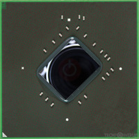
The Quadro M520 Mobile was a professional mobile graphics chip by NVIDIA, launched on January 11th, 2017. Built on the 28 nm process, and based on the GM108 graphics processor, the chip supports DirectX 12. The GM108 graphics processor is a relatively small chip with a die area of only 77 mm² and 1,020 million transistors. It features 384 shading units, 16 texture mapping units, and 8 ROPs. NVIDIA has paired 2,048 MB GDDR5 memory with the Quadro M520 Mobile, which are connected using a 64-bit memory interface. The GPU is operating at a frequency of 965 MHz, which can be boosted up to 1176 MHz, memory is running at 1253 MHz (5 Gbps effective).
Being a mxm module card, the NVIDIA Quadro M520 Mobile does not require any additional power connector, its power draw is rated at 25 W maximum. This device has no display connectivity, as it is not designed to have monitors connected to it. Rather it is intended for use in laptop/notebooks and will use the output of the host mobile device.
Being a mxm module card, the NVIDIA Quadro M520 Mobile does not require any additional power connector, its power draw is rated at 25 W maximum. This device has no display connectivity, as it is not designed to have monitors connected to it. Rather it is intended for use in laptop/notebooks and will use the output of the host mobile device.
Graphics Processor
Mobile Graphics
- Release Date
- Jan 11th, 2017
- Generation
-
Quadro Maxwell-M
(Mx200)
- Predecessor
- Quadro Kepler-M
- Successor
- Quadro Pascal-M
- Production
- End-of-life
- Bus Interface
- MXM-A (3.0)
- Reviews
- 26 in our database
Relative Performance
Based on TPU review data: "Performance Summary" at 1920x1080, 4K for 2080 Ti and faster.
Performance estimated based on architecture, shader count and clocks.
Clock Speeds
- Base Clock
- 965 MHz
- Boost Clock
- 1176 MHz
- Memory Clock
-
1253 MHz
5 Gbps effective
Memory
- Memory Size
- 2 GB
- Memory Type
- GDDR5
- Memory Bus
- 64 bit
- Bandwidth
- 40.10 GB/s
Render Config
- Shading Units
- 384
- TMUs
- 16
- ROPs
- 8
- SMM Count
- 2
- L1 Cache
- 64 KB (per SMM)
- L2 Cache
- 1024 KB
Theoretical Performance
- Pixel Rate
- 9.408 GPixel/s
- Texture Rate
- 18.82 GTexel/s
- FP32 (float)
- 903.2 GFLOPS
- FP64 (double)
- 28.22 GFLOPS (1:32)
Board Design
- Slot Width
- MXM Module
- TDP
- 25 W
- Outputs
- Portable Device Dependent
- Power Connectors
- None
Graphics Features
- DirectX
- 12 (11_0)
- OpenGL
- 4.6
- OpenCL
- 3.0
- Vulkan
- 1.3
- CUDA
- 5.0
- Shader Model
- 6.7 (5.1)
GM108 GPU Notes
| NVENC: No Support NVDEC: No Support PureVideo HD: VP6 VDPAU: Feature Set E Latest Drivers: Windows Vista: GeForce Release 365.19 Quadro Release R346 U7 (348.40) / R352 BETA (352.86) Windows 7 / 8 / 8.1 (x32 / x64): GeForce Release 391.35 / 474.89 GeForce Mobile Release 391.35 / 425.31 Quadro Release R390 U9 (392.37) / R440 U4 (441.66) Quadro Mobile Release R390 U9 (392.37) / R418 U9 (426.78) WIndows 10 / 11 (x32 / x64): GeForce Release 391.35 / 474.89 GeForce Mobile Release 391.35 / 425.31 Quadro Release R390 U9 (392.37) / R470 U16 (474.82) Quadro Mobile Release R390 U9 (392.37) / R418 U9 (426.78) |
Devices based on this design (1)
| Name | GPU Clock | Boost Clock | Memory Clock | Other Changes |
|---|---|---|---|---|
| 1354 MHz | 1493 MHz | 1752 MHz | 4 GB |
Apr 8th, 2025 02:59 EDT
change timezone
Latest GPU Drivers
New Forum Posts
- The coffee and tea drinkers club. (249)
- 9070XT or 7900XT or 7900XTX (124)
- Free Games Thread (4611)
- USB case with dual USB-C and dual USB-A (9)
- gpu heirarchy/performance/benchmarks- whos lying? (65)
- Anyone with true HDDs still around here? (338)
- Kindly help in Identifying GPU and Suitable bios (9)
- AMD RX 9070 XT & RX 9070 non-XT thread (OC, undervolt, benchmarks, ...) (84)
- 12v lines 0 reads occansionally (3)
- Asus X670E Crosshair Crashes (7)
Popular Reviews
- The Last Of Us Part 2 Performance Benchmark Review - 30 GPUs Compared
- UPERFECT UStation Delta Max Review - Two Screens In One
- ASUS Prime X870-P Wi-Fi Review
- PowerColor Radeon RX 9070 Hellhound Review
- Upcoming Hardware Launches 2025 (Updated Apr 2025)
- MCHOSE L7 Pro Review
- Sapphire Radeon RX 9070 XT Pulse Review
- Corsair RM750x Shift 750 W Review
- Sapphire Radeon RX 9070 XT Nitro+ Review - Beating NVIDIA
- DDR5 CUDIMM Explained & Benched - The New Memory Standard
Controversial News Posts
- NVIDIA GeForce RTX 5060 Ti 16 GB SKU Likely Launching at $499, According to Supply Chain Leak (161)
- MSI Doesn't Plan Radeon RX 9000 Series GPUs, Skips AMD RDNA 4 Generation Entirely (146)
- Microsoft Introduces Copilot for Gaming (124)
- AMD Radeon RX 9070 XT Reportedly Outperforms RTX 5080 Through Undervolting (119)
- NVIDIA Reportedly Prepares GeForce RTX 5060 and RTX 5060 Ti Unveil Tomorrow (115)
- Over 200,000 Sold Radeon RX 9070 and RX 9070 XT GPUs? AMD Says No Number was Given (100)
- NVIDIA GeForce RTX 5050, RTX 5060, and RTX 5060 Ti Specifications Leak (97)
- Nintendo Switch 2 Launches June 5 at $449.99 with New Hardware and Games (92)

