Apr 10th, 2025 04:23 EDT
change timezone
Latest GPU Drivers
New Forum Posts
- [Update] FanControl (and other different monitoring software) blocked by Defender due to Winring0 vulnerability (2)
- Do you use Linux? (572)
- Help with updating firmware on a AOC Agon Pro OLED monitor, says I need Install Tool (3)
- HP EliteDesk 800 G2 SFF CPU support (2)
- Anyone know where to get driver updates / backdates for TUF A15? (4)
- EK Quantum Velocity intel to amd conversion (13)
- How is the Gainward Phoenix Model in terms of quality? (0)
- ## [Golden Sample] RTX 5080 – 3300 MHz @ 1.020 V (Stock Curve) – Ultra-Stable & Efficient (44)
- hp envy 15 rtx 2060 max-q stock vbios (1)
- (Some of) What I'd like to See From a Final Fantasy IX Remake (10)
Popular Reviews
- The Last Of Us Part 2 Performance Benchmark Review - 30 GPUs Compared
- ASRock Z890 Taichi OCF Review
- MCHOSE L7 Pro Review
- Sapphire Radeon RX 9070 XT Pulse Review
- PowerColor Radeon RX 9070 Hellhound Review
- Upcoming Hardware Launches 2025 (Updated Apr 2025)
- Sapphire Radeon RX 9070 XT Nitro+ Review - Beating NVIDIA
- Acer Predator GM9000 2 TB Review
- ASUS GeForce RTX 5080 Astral OC Review
- UPERFECT UStation Delta Max Review - Two Screens In One
Controversial News Posts
- NVIDIA GeForce RTX 5060 Ti 16 GB SKU Likely Launching at $499, According to Supply Chain Leak (174)
- MSI Doesn't Plan Radeon RX 9000 Series GPUs, Skips AMD RDNA 4 Generation Entirely (146)
- Microsoft Introduces Copilot for Gaming (124)
- AMD Radeon RX 9070 XT Reportedly Outperforms RTX 5080 Through Undervolting (119)
- NVIDIA Reportedly Prepares GeForce RTX 5060 and RTX 5060 Ti Unveil Tomorrow (115)
- Over 200,000 Sold Radeon RX 9070 and RX 9070 XT GPUs? AMD Says No Number was Given (100)
- Nintendo Switch 2 Launches June 5 at $449.99 with New Hardware and Games (99)
- Nintendo Confirms That Switch 2 Joy-Cons Will Not Utilize Hall Effect Stick Technology (99)
News Posts matching #20nm
Return to Keyword BrowsingAmidst Production Woes, Pricing of DDR4 DRAM to Climb 12.5% on 2Q17 - Trendforce
Continuing the trend of previous reports, DRAMeXchange, a division of TrendForce, reports the general price increase in the PC DRAM market is growing larger than anticipated as the already tight supply situation is compounded by quality problems with products made on the leading-edge processes. Based on a preliminary survey of completed contracts for the second quarter, DRAMeXchange estimates that the average contract price of 4GB DDR4 modules will go up by about 12.5% compared with the first quarter, from US$24 to around US$27.
"PC-OEMs that have been negotiating their second-quarter memory contracts initially expected the market supply to expand because Samsung and Micron have begun to produce on the 18 nm and the 17 nm processes, respectively," said Avril Wu, research director of DRAMeXchange. "However, both Samsung and Micron have encountered setbacks related to sampling and yield, so the supply situation remains tight going into the second quarter and PC DRAM prices will continue to rise through this three-month period."
"PC-OEMs that have been negotiating their second-quarter memory contracts initially expected the market supply to expand because Samsung and Micron have begun to produce on the 18 nm and the 17 nm processes, respectively," said Avril Wu, research director of DRAMeXchange. "However, both Samsung and Micron have encountered setbacks related to sampling and yield, so the supply situation remains tight going into the second quarter and PC DRAM prices will continue to rise through this three-month period."


Micron's Outlook for the Future of Memory: GDDR6, QuantX in 2017
After finally reaching mature yields (comparable to those of planar NAND processes), Micron's 32-layer first generation 3D NAND has grown increasingly prominent in the company's NAND output. Now, the company is looking to ramp-up production of their (currently sampling) 64-layer 3D NAND, promising "meaningful output" by the end of December 2017, looking for an 80% increase in total GB per wafer and a 30% decrease in production costs.
When it comes to the graphics subsystem memory, Micron is looking to transition their 20nm production to a "1x nm" (most likely 16nm) node, in a bid to improve cost per GB by around $20, with introduction of 16nm GDDR5 memory to be introduced later this year. However, GDDR5X volume is expected to grow significantly, in a bid to satisfy bandwidth-hungry uses through GPUs (like NVIDIA's GTX 1080 and potentially the upcoming 1080 Ti) and networking, with GDDR6 memory being introduced by the end of 2017 or early 2018. The company is still mum on actual consumer products based on their interpretation of the 3D XPoint products through their QuantX brand, though work is already under way on the second and third generation specifications of this memory, with Micron planning an hitherto unknown (in significance and product type) presence in the consumer market by the end of this year.

When it comes to the graphics subsystem memory, Micron is looking to transition their 20nm production to a "1x nm" (most likely 16nm) node, in a bid to improve cost per GB by around $20, with introduction of 16nm GDDR5 memory to be introduced later this year. However, GDDR5X volume is expected to grow significantly, in a bid to satisfy bandwidth-hungry uses through GPUs (like NVIDIA's GTX 1080 and potentially the upcoming 1080 Ti) and networking, with GDDR6 memory being introduced by the end of 2017 or early 2018. The company is still mum on actual consumer products based on their interpretation of the 3D XPoint products through their QuantX brand, though work is already under way on the second and third generation specifications of this memory, with Micron planning an hitherto unknown (in significance and product type) presence in the consumer market by the end of this year.


Samsung Mass-producing First 128GB DDR4 RDIMM for Servers
Samsung Electronics Co., Ltd., announced today that it is mass producing the industry's first "through silicon via" (TSV) double data rate-4 (DDR4) memory in 128-gigabyte (GB) modules, for enterprise servers and data centers. Following Samsung's introduction of the world-first 3D TSV DDR4 DRAM (64GB) in 2014, the company's new TSV registered dual inline memory module (RDIMM) marks another breakthrough that opens the door for ultra-high capacity memory at the enterprise level. Samsung's new TSV DRAM module boasts the largest capacity and the highest energy efficiency of any DRAM modules today, while operating at high speed and demonstrating excellent reliability.
"We are pleased that volume production of our high speed, low-power 128GB TSV DRAM module will enable our global IT customers and partners to launch a new generation of enterprise solutions with dramatically improved efficiency and scalability for their investment," said Joo Sun Choi, executive vice president, Memory Sales and Marketing, Samsung Electronics. "We will continue to expand our technical cooperation with global leaders in servers, consumer electronics and emerging markets, where consumers can benefit from innovative technology that enhances their productivity and the overall user experience."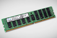
"We are pleased that volume production of our high speed, low-power 128GB TSV DRAM module will enable our global IT customers and partners to launch a new generation of enterprise solutions with dramatically improved efficiency and scalability for their investment," said Joo Sun Choi, executive vice president, Memory Sales and Marketing, Samsung Electronics. "We will continue to expand our technical cooperation with global leaders in servers, consumer electronics and emerging markets, where consumers can benefit from innovative technology that enhances their productivity and the overall user experience."


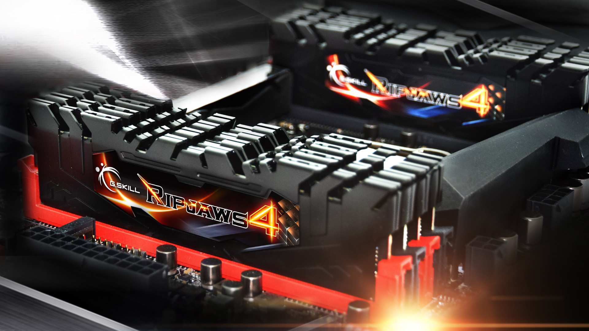
G.SKILL Announces the World's Fastest DDR4 128GB (8x 16GB) Memory Kit
G.SKILL International Enterprises Co., Ltd., the world's leading manufacturer of extreme performance memory and solid state storage, is thrilled to announce the world's first DDR4 128GB(16GBx8) 2800MHz CL16-16-16 -36 1.35V memory kit based on the newest 16GB capacity DDR4 consumer-class memory modules. These high capacity memory modules are manufactured with new 8Gb ICs produced on the latest 20nm fabrication process, which takes performance to a whole new level, by Samsung Electronics.
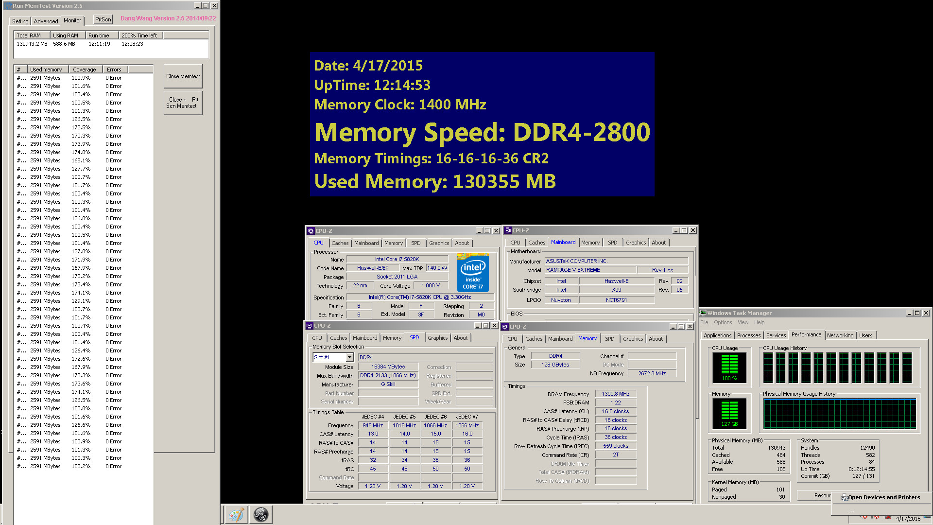
While 16GB capacity have been available for server memory in the past, support and design for such large capacity memory modules are now paving its way to consumer memory modules, suitable for workstation level workloads where high capacity memory is vital. These new G.SKILL Ripjaws 4 series high capacity memory kits are capable of running in quad-channel at a grand total of 128GB, and have already been validated on the latest ASUS X99 Rampage V Extreme motherboard with Intel Haswell-E processors. A stress-testing screenshot of the newly released memory kit with 16GB DDR4 modules can be found below.
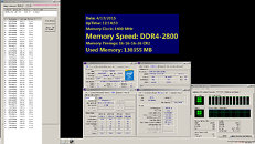
While 16GB capacity have been available for server memory in the past, support and design for such large capacity memory modules are now paving its way to consumer memory modules, suitable for workstation level workloads where high capacity memory is vital. These new G.SKILL Ripjaws 4 series high capacity memory kits are capable of running in quad-channel at a grand total of 128GB, and have already been validated on the latest ASUS X99 Rampage V Extreme motherboard with Intel Haswell-E processors. A stress-testing screenshot of the newly released memory kit with 16GB DDR4 modules can be found below.
Samsung Starts Mass Producing Industry's First 8 Gb GDDR5 Memory
Samsung Electronics Co., Ltd., the world leader in advanced memory technology, announced today that it has begun mass producing the industry's first 8 gigabit (Gb) GDDR5 DRAM, based on the company's leading-edge 20-nanometer (nm) process technology. GDDR5 is the most widely used discrete graphics memory in the world.
Designed for use in graphics cards for PCs and supercomputing applications, and on-board graphics memory for game consoles and notebook PCs, discrete graphics DRAM provides an extensive amount of bandwidth to process large high quality graphically-oriented data streams. With the rising popularity of 3-D games and UHD video content soon to be widespread, the need for high-performance, high-bandwidth graphics memory has begun to rapidly increase.
Designed for use in graphics cards for PCs and supercomputing applications, and on-board graphics memory for game consoles and notebook PCs, discrete graphics DRAM provides an extensive amount of bandwidth to process large high quality graphically-oriented data streams. With the rising popularity of 3-D games and UHD video content soon to be widespread, the need for high-performance, high-bandwidth graphics memory has begun to rapidly increase.

Samsung Starts Mass-producing First 8 Gigabit LPDDR4 Mobile DRAM
Samsung Electronics Co., Ltd., the world leader in advanced memory technology, announced today that it has started mass producing the industry's first 8 gigabit (Gb), low power double data rate 4 (LPDDR4) mobile DRAM based on the company's leading-edge 20-nanometer (nm) process technology. LPDDR memories are the most widely used "working memory" for mobile devices worldwide.
"By initiating production of 20nm 8Gb LPDDR4, which is even faster than the DRAM for PCs and servers and consumes much less energy, we are contributing to the timely launch of UHD, large-screen flagship mobile devices," said Joo Sun Choi, Executive Vice President of Memory Sales and Marketing at Samsung Electronics. "As this major advancement in mobile memory demonstrates, we will continue to closely collaborate with global mobile device manufacturers to optimize DRAM solutions, making them suitable for next-generation mobile OS environments."
"By initiating production of 20nm 8Gb LPDDR4, which is even faster than the DRAM for PCs and servers and consumes much less energy, we are contributing to the timely launch of UHD, large-screen flagship mobile devices," said Joo Sun Choi, Executive Vice President of Memory Sales and Marketing at Samsung Electronics. "As this major advancement in mobile memory demonstrates, we will continue to closely collaborate with global mobile device manufacturers to optimize DRAM solutions, making them suitable for next-generation mobile OS environments."

Intel Custom Foundry Demos Industry-Leading 32 Gbps SerDes on 14 nm Process
Intel Corporation today unveiled silicon characterization results for its 1 to 32 Gbps high-speed SerDes on the 14nm process. This 32 Gbps SerDes is the second SerDes offering and adds to the previously announced 1 to 16 Gbps GP 14nm SerDes. It will be available by end of this year.
Intel's 14nm SerDes family is the second generation of SerDes offering and is built on the success of Intel's 12 and 28 Gbps SerDes, which is currently in production on Intel's 22nm Tri-gate process technology. Intel's 14nm SerDes extends the operating range while reducing power by 20 percent and area by more than 40 percent as compared to Intel's 22nm SerDes offering. This announcement marks the first time that a 32 Gbps, multiprotocol SerDes has been validated on any sub-20nm foundry process.
Intel's 14nm SerDes family is the second generation of SerDes offering and is built on the success of Intel's 12 and 28 Gbps SerDes, which is currently in production on Intel's 22nm Tri-gate process technology. Intel's 14nm SerDes extends the operating range while reducing power by 20 percent and area by more than 40 percent as compared to Intel's 22nm SerDes offering. This announcement marks the first time that a 32 Gbps, multiprotocol SerDes has been validated on any sub-20nm foundry process.
Samsung Now Mass Producing Industry's First 20-Nanometer 6Gb LPDDR3 Mobile DRAM
Samsung Electronics Co., Ltd., the world leader in advanced memory technology, announced today that it has begun mass producing its six gigabit (Gb) low-power double data rate 3 (LPDDR3) mobile DRAM, based on advanced 20 nanometer (nm) process technology. The highly-efficient new mobile memory chip will enable longer battery run-time and faster application loading on large screen mobile devices with higher resolution.
"Our new 20nm 6Gb LPDDR3 DRAM provides the most advanced mobile memory solution for the rapidly expanding high-performance mobile DRAM market," said Jeeho Baek, vice president, memory marketing, Samsung Electronics. "We are working closely with our global customers to offer next-generation mobile memory solutions that can be applied to a more extensive range of markets ranging from the premium to standard segments."
Samsung's new 6Gb LPDDR3 has a per-pin data transfer rate of up to 2,133 megabits per second (Mbps). A 3GB (gigabyte) LPDDR3 package, which consists of four 6Gb LPDDR3 chips, can be easily created for use in a wide range of mobile devices. Also, the package greatly strengthens our product portfolio for premium mobile applications.
Samsung Now Mass Producing Industry's Most Advanced DDR4
Samsung Electronics Co., Ltd., the world leader in advanced memory technology, today announced that it is mass producing the most advanced DDR4 memory, for enterprise servers in next-generation data centers.
With the introduction of these high-performance, high-density DDR4 modules, Samsung can better support the need for advanced DDR4 in rapidly expanding, large-scale data centers and other enterprise server applications.
With the introduction of these high-performance, high-density DDR4 modules, Samsung can better support the need for advanced DDR4 in rapidly expanding, large-scale data centers and other enterprise server applications.

Samsung Introduces World's First 3D V-NAND Based SSD for Enterprise Applications
Samsung Electronics Co., Ltd., the world leader in advanced memory technology, today introduced the first solid state drive (SSD) based on its industry-leading 3D V-NAND technology. Samsung announced its new SSD, designed for use in enterprise servers and data centers, during a keynote at the Flash Memory Summit 2013 here.
"By applying our 3D V-NAND - which has overcome the formidable hurdle of scaling beyond the 10-nanometer (nm) class*, Samsung is providing its global customers with high density and exceptional reliability, as well as an over 20 percent performance increase and an over 40 percent improvement in power consumption," said E.S. Jung, executive vice president, semiconductor R&D center at Samsung Electronics and a keynote speaker at the Flash Memory Summit. "As we pioneer a new era of memory technology, we will continue to introduce differentiated green memory products and solutions for the server, mobile and PC markets to help reduce energy waste and to create greater shared value in the enterprise and for consumers."
"By applying our 3D V-NAND - which has overcome the formidable hurdle of scaling beyond the 10-nanometer (nm) class*, Samsung is providing its global customers with high density and exceptional reliability, as well as an over 20 percent performance increase and an over 40 percent improvement in power consumption," said E.S. Jung, executive vice president, semiconductor R&D center at Samsung Electronics and a keynote speaker at the Flash Memory Summit. "As we pioneer a new era of memory technology, we will continue to introduce differentiated green memory products and solutions for the server, mobile and PC markets to help reduce energy waste and to create greater shared value in the enterprise and for consumers."


SK Hynix Develops the World's First High Density 8 Gb LPDDR3
SK Hynix Inc. announced that it has developed the world's first 8 Gb(Gigabit) LPDDR3 (Low Power DDR3) using its advanced 20nm class process technology. This product is a top-performance mobile memory solution which features high density, ultrahigh speed and low power consumption.
The new products can be stacked up and realize a high density of maximum 4 GB(Gigabytes, 32 Gb) solution in a single package. In addition, the height of this package becomes dramatically thinner than the existing 4 Gb-based one. In terms of its high density and competitive package height, it is suitable for the newest trend of the mobile applications.
The new products can be stacked up and realize a high density of maximum 4 GB(Gigabytes, 32 Gb) solution in a single package. In addition, the height of this package becomes dramatically thinner than the existing 4 Gb-based one. In terms of its high density and competitive package height, it is suitable for the newest trend of the mobile applications.

GLOBALFOUNDRIES Accelerates Adoption of 20nm-LPM and 14nm-XM FinFET Processes
At next week's 50th Design Automation Conference (DAC) in Austin, Texas, GLOBALFOUNDRIES will unveil a comprehensive set of certified design flows to support its most advanced manufacturing processes. The flows, jointly developed with the leading EDA providers, offer robust support for implementing designs in the company's 20nm low power process and its leading-edge 14nm-XM FinFET process. Working closely with Cadence Design Systems, Mentor Graphics and Synopsys, GLOBALFOUNDRIES has developed the flows to address the most pressing design challenges, including support for analog/mixed signal (AMS) design, and advanced digital designs, both with demonstration of the impact of double patterning on the flow.
The GLOBALFOUNDRIES design flows work with its process design kits (PDKs) to provide real examples that demonstrate the entire flow. The user can download the design database, the PDK, detailed documentation and multi-vendor scripts to learn how to set up and use the GLOBALFOUNDRIES design flow. The flows use open source examples and provide the customer with working, executable and customizable flows.
The GLOBALFOUNDRIES design flows work with its process design kits (PDKs) to provide real examples that demonstrate the entire flow. The user can download the design database, the PDK, detailed documentation and multi-vendor scripts to learn how to set up and use the GLOBALFOUNDRIES design flow. The flows use open source examples and provide the customer with working, executable and customizable flows.
Samsung Now Producing 4 Gb LPDDR3 Mobile DRAM, Using 20nm-class Process Technology
Samsung Electronics Co., Ltd., the world leader in advanced memory technology, today announced the industry's first production of ultra-high-speed four gigabit (Gb) low power double data rate 3 (LPDDR3) mobile DRAM, which is being produced at a 20 nanometer (nm) class* process node. The new 4Gb LPDDR3 mobile DRAM enables performance levels comparable to the standard DRAM utilized in personal computers, making it an attractive solution for demanding multimedia-intensive features on next-generation mobile devices such as high-performance smartphones and tablets.
"By providing the most efficient next-generation mobile memory with a very large data capacity, we are now enabling OEMs to introduce even more innovative designs in the marketplace," said Young-Hyun Jun, executive vice president, memory sales & marketing, Samsung Electronics. "Our 20nm-class four gigabit mobile DRAM provides another example of our ability to deliver well-differentiated, high-performance, high-density memory to customers in a timely manner."
"By providing the most efficient next-generation mobile memory with a very large data capacity, we are now enabling OEMs to introduce even more innovative designs in the marketplace," said Young-Hyun Jun, executive vice president, memory sales & marketing, Samsung Electronics. "Our 20nm-class four gigabit mobile DRAM provides another example of our ability to deliver well-differentiated, high-performance, high-density memory to customers in a timely manner."
GLOBALFOUNDRIES Demonstrates 3D TSV Capabilities on 20nm Technology
GLOBALFOUNDRIES today announced the accomplishment of a key milestone in its strategy to enable 3D stacking of chips for next-generation mobile and consumer applications. At its Fab 8 campus in Saratoga County, N.Y., the company has demonstrated its first functional 20nm silicon wafers with integrated Through-Silicon Vias (TSVs). Manufactured using GLOBALFOUNDRIES' leading-edge 20nm-LPM process technology, the TSV capabilities will allow customers to stack multiple chips on top of each other, providing another avenue for delivering the demanding performance, power, and bandwidth requirements of today's electronic devices.
TSVs are vertical vias etched in a silicon wafer that are filled with a conducting material, enabling communication between vertically stacked integrated circuits. The adoption of three-dimensional (3D) chip stacking is increasingly being viewed as an alternative to traditional technology node scaling at the transistor level. However, TSVs present a number of new challenges to semiconductor manufacturers.
TSVs are vertical vias etched in a silicon wafer that are filled with a conducting material, enabling communication between vertically stacked integrated circuits. The adoption of three-dimensional (3D) chip stacking is increasingly being viewed as an alternative to traditional technology node scaling at the transistor level. However, TSVs present a number of new challenges to semiconductor manufacturers.

Western Digital Makes Strategic Investment in Skyera
Skyera Inc. and Western Digital Corp. (NASDAQ: WDC) today announced that Skyera has received strategic funding from Western Digital Capital as part of its recently announced Series B round of financing. Western Digital Capital co-invested in the $51 million round as an extension of the strategic relationship between the two companies that also includes joint technology development. Western Digital had previously funded Skyera as its initial outside investor.
"The backing of Western Digital has enabled us to ramp our business across marketing, sales and engineering which has been instrumental in creating the industry's most innovative solid-state solution," said Radoslav Danilak , chief executive officer of Skyera. "With our skyHawk family of enterprise solid-state storage systems we are witnessing the next era of solid-state storage and I strongly believe that having a close working relationship with Western Digital, the world's top disk drive vendor, is invaluable as we set out to reshape the storage landscape."
"The backing of Western Digital has enabled us to ramp our business across marketing, sales and engineering which has been instrumental in creating the industry's most innovative solid-state solution," said Radoslav Danilak , chief executive officer of Skyera. "With our skyHawk family of enterprise solid-state storage systems we are witnessing the next era of solid-state storage and I strongly believe that having a close working relationship with Western Digital, the world's top disk drive vendor, is invaluable as we set out to reshape the storage landscape."

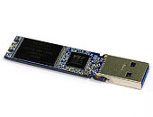
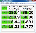
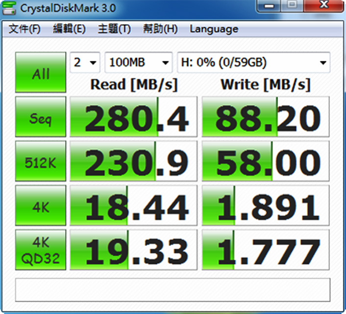
VIA Labs Announces Next-Generation USB 3.0 to NAND Flash Controllers
VIA Labs, Inc., a leading supplier of USB 3.0 integrated chip controllers, today announced its two latest USB 3.0 device controllers, the VIA VL752 and VIA VL753 SuperSpeed USB 3.0 to NAND flash controllers. The VIA VL752 and VIA VL753 deliver enhanced performance using the latest NAND flash technologies including 19nm, 20nm and 21nm geometries and have been certified by the USB Implementers Forum (USB-IF) for SuperSpeed operation, ensuring high quality, seamless interoperability, and effortless backwards compatibility.
The two-channel the VIA VL752 and single-channel VIA VL753 offer data transfer speeds up to 280MB/s, flexible bad block management, support for the latest 200MHz DDR NAND Flash, and a robust ECC engine for greater data integrity. The package sizes from the previous generation of VIA Superspeed USB to NAND flash controllers have been reduced to a QFN68 8 x 8mm package for the VIA VL752 and a QFN48 6 x 6mm package for the VIA VL753 to enable the smallest form-factor designs.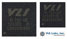
The two-channel the VIA VL752 and single-channel VIA VL753 offer data transfer speeds up to 280MB/s, flexible bad block management, support for the latest 200MHz DDR NAND Flash, and a robust ECC engine for greater data integrity. The package sizes from the previous generation of VIA Superspeed USB to NAND flash controllers have been reduced to a QFN68 8 x 8mm package for the VIA VL752 and a QFN48 6 x 6mm package for the VIA VL753 to enable the smallest form-factor designs.


NVIDIA to Pull Through 2013 with Kepler Refresh, "March of Maxwell" in 2014
Those familiar with "Maxwell," codename for NVIDIA's next-generation GPU architecture, will find the new company roadmap posted below slightly different. For one, Maxwell is given a new launch timeframe, in 2014. Following this year's successful run at the markets with the Kepler family of GPUs, NVIDIA is looking up to Kepler Refresh GK11x family of GPUs to lead the company's product lineup in 2013. The new GPUs will arrive in the first half of next year, most likely in March, and will be succeeded by the Maxwell family of GPUs in 2014. Apart from the fact that Kepler established good performance and energy-efficiency leads over competitive architectures, a reason behind Maxwell's 2014 launch could be technical. We know from older reports that TSMC, NVIDIA's principal foundry partner, will begin mass production of 20 nanometer chips only by Q4-2013.

Micron 20 nm NAND Flash Powers Skyhawk Enterprise SSD
Micron Technology, Inc. today announced another new storage industry milestone-the integration of its 20nm NAND flash storage media into a high-endurance, high-capacity enterprise system. San Jose-based Skyera is using Micron's 20nm, 128 gigabit (Gb) multilevel cell (MLC) NAND flash storage media to pack an astounding 44 terabytes (TB) into a single, compact enterprise storage system for big data, cloud computing, and virtualization applications. Skyera's Skyhawk system uses more than 3,000 Micron flash storage components, creating a high-capacity, high-performance storage solution that fits into a 1U form factor-about the size of a pizza box.
Both the end system and the components have earned industry awards for innovation. The Skyhawk storage system's impressive capabilities earned it Best of Show at this year's Flash Memory Summit in August. In February, UBM TechInsights recognized Micron's groundbreaking 20nm MLC NAND (developed jointly with Intel); giving it their top honor-Semiconductor of the Year. This 20nm process technology is critical to creating storage media with the capacity, endurance, and cost-effectiveness required for enterprise storage on this scale-and Micron's device is the only MLC NAND available in a 128 Gb density.
Both the end system and the components have earned industry awards for innovation. The Skyhawk storage system's impressive capabilities earned it Best of Show at this year's Flash Memory Summit in August. In February, UBM TechInsights recognized Micron's groundbreaking 20nm MLC NAND (developed jointly with Intel); giving it their top honor-Semiconductor of the Year. This 20nm process technology is critical to creating storage media with the capacity, endurance, and cost-effectiveness required for enterprise storage on this scale-and Micron's device is the only MLC NAND available in a 128 Gb density.
SK Hynix Introduces DDR3L-Reduced Standby for Mobile Solutions
SK Hynix announced that it has introduced DDR3L-RS (Reduced Standby) DRAM for mobile solutions using its 20nm class technology. This product significantly reduces the standby power consumption.
By using cutting-edge 20nm class technology and efficiently managing standby current, this DDR3L-RS product reduces 70% of standby power compared to existing DDR3L DRAM while it maintains DDR3L performance. DDR3L DRAM which has recently gone mainstream works at 1.35V, while DDR3 DRAM does at 1.5V.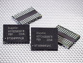
By using cutting-edge 20nm class technology and efficiently managing standby current, this DDR3L-RS product reduces 70% of standby power compared to existing DDR3L DRAM while it maintains DDR3L performance. DDR3L DRAM which has recently gone mainstream works at 1.35V, while DDR3 DRAM does at 1.5V.
ARM and GLOBALFOUNDRIES Collaborate to Enable Devices on 20 nm and FinFET
GLOBALFOUNDRIES and ARM today announced a multi-year agreement to jointly deliver optimized system-on-chip (SoC) solutions for ARM processor designs on GLOBALFOUNDRIES' 20-nanometer (nm) and FinFET process technologies. The new agreement also extends the long-standing collaboration to include graphics processors, which are becoming an increasingly critical component in mobile devices. As part of the agreement, ARM will develop a full platform of ARM Artisan Physical IP, including standard cell libraries, memory compilers and POP IP solutions. The results will help enable a new level of system performance and power-efficiency for a range of mobile applications, from smartphones to tablets to ultra-thin notebooks.
The companies have been collaborating for several years to jointly optimize ARM Cortex-A series processors, including multiple demonstrations of performance and power-efficiency benefits on 28nm as well as a 20nm test-chip implementation currently running through GLOBALFOUNDRIES fab in Malta, N.Y. This agreement extends the prior efforts by driving production IP platforms that will enable customer designs on 20nm and promote rapid migration to three-dimensional FinFET transistor technology. This joint development will enable a faster time to delivering SoC solutions for customers using next-generation ARM CPUs and GPUs in mobile devices.
The companies have been collaborating for several years to jointly optimize ARM Cortex-A series processors, including multiple demonstrations of performance and power-efficiency benefits on 28nm as well as a 20nm test-chip implementation currently running through GLOBALFOUNDRIES fab in Malta, N.Y. This agreement extends the prior efforts by driving production IP platforms that will enable customer designs on 20nm and promote rapid migration to three-dimensional FinFET transistor technology. This joint development will enable a faster time to delivering SoC solutions for customers using next-generation ARM CPUs and GPUs in mobile devices.
SK Hynix to Launch Client-side SSD in the US
SK Hynix announced its launch of client SSD (Solid State Drive). The SSD features faster speed and low power consumption than HDD (Hard Disk Drive) so it is expected to replace the HDD as another type of storage for PCs and other applications.
The first ever SK Hynix's client 2.5" SSD consists of ONFI synchronous NAND Flash memory using 20nm class process and densities of 128GB (Gigabyte) and 256GB are available. It significantly improves the speed and reliability by adopting SATA III interface with data transmissions at 6Gb/s (Gigabits per second). This high performance SSD generates sequential read speeds of 510MB/s (Megabytes per second) and sequential write speeds of 470MB/s. It is three or four times faster than the traditional HDD.
The first ever SK Hynix's client 2.5" SSD consists of ONFI synchronous NAND Flash memory using 20nm class process and densities of 128GB (Gigabyte) and 256GB are available. It significantly improves the speed and reliability by adopting SATA III interface with data transmissions at 6Gb/s (Gigabits per second). This high performance SSD generates sequential read speeds of 510MB/s (Megabytes per second) and sequential write speeds of 470MB/s. It is three or four times faster than the traditional HDD.

Samsung Electronics Announces New 300 mm Logic Line in Korea
Samsung Electronics Co. Ltd., a world leader in advanced semiconductor solutions, today announced plans to build a new fabrication line in Hwaseong, South Korea, to meet the growing demands for logic products. Samsung will invest 2.25 trillion Korean won in the new fabrication line, which will break ground this month with a target timeline for completion by the end of 2013.
The new fabrication line will mainly produce highly advanced mobile application processors on 300mm wafers at 20nm and 14nm process nodes. Along with Lines 9 and 14, which have been converted to System LSI fabrication earlier this year, the new line will help supply to the expanding need for smart mobile solutions.
The new fabrication line will mainly produce highly advanced mobile application processors on 300mm wafers at 20nm and 14nm process nodes. Along with Lines 9 and 14, which have been converted to System LSI fabrication earlier this year, the new line will help supply to the expanding need for smart mobile solutions.
GLOBALFOUNDRIES Silicon Validates 28nm AMS Production Design
At next week's Design Automation Conference (DAC) in San Francisco, Calif., GLOBALFOUNDRIES plans to demonstrate an enhanced silicon-validated design flow for its 28nm Super Low Power (SLP) technology with Gate First High-k Metal Gate (HKMG). The flow provides proven and complete front-to-back support for advanced analog/mixed-signal (AMS) design using the industry's latest design automation technology. In addition, the company will reveal jointly developed design flows with its EDA partners in certifying both analog and digital "double patterning aware" flows for its 20nm process, with silicon validation expected in early 2013 at that technology node.
As a result of GLOBALFOUNDRIES' commitment to silicon validation of flows before releasing them, customers have the confidence to produce signoff-ready 28nm digital and analog designs using the industry's most advanced set of design tools, tool scripts, and methodologies from the leading EDA suppliers. The company's tight collaboration with the design tool and IP ecosystem also accelerates its ability to develop working flows for advanced nodes such as 20nm, providing their advantages in gate density, performance, and lower power to customers ahead of other foundries.
As a result of GLOBALFOUNDRIES' commitment to silicon validation of flows before releasing them, customers have the confidence to produce signoff-ready 28nm digital and analog designs using the industry's most advanced set of design tools, tool scripts, and methodologies from the leading EDA suppliers. The company's tight collaboration with the design tool and IP ecosystem also accelerates its ability to develop working flows for advanced nodes such as 20nm, providing their advantages in gate density, performance, and lower power to customers ahead of other foundries.
Samsung Now Producing Highest Density Mobile LPDDR2 Using 20nm-class Technology
Samsung Electronics Co., Ltd., a global leader in advanced semiconductor technology solutions, announced today that it has begun producing the industry's first four gigabit (Gb), low power double-data-rate 2 (LPDDR2) memory using 20 nanometer (nm) class* technology. The mobile DRAM (dynamic random access memory) chip, which went into mass production last month, will help the market to deliver advanced devices that are faster, lighter and provide longer battery life than today's mobile devices.
"Samsung began expanding the market for 4Gb DRAM last year with the first mass-produced 30nm-class DRAM, and now we are working on capturing most of the advanced memory market with our new 20nm-class 4Gb DRAM," said Wanhoon Hong, executive vice president, memory sales & marketing, Samsung Electronics. "In the second half of this year, we expect to strongly increase the portion of 20nm-class DRAM within our overall DRAM output to make the 4Gb DRAM line-up the mainstream product in DRAM production, and therefore keeping the leadership position in the premium market and strengthening our competitive edge."
"Samsung began expanding the market for 4Gb DRAM last year with the first mass-produced 30nm-class DRAM, and now we are working on capturing most of the advanced memory market with our new 20nm-class 4Gb DRAM," said Wanhoon Hong, executive vice president, memory sales & marketing, Samsung Electronics. "In the second half of this year, we expect to strongly increase the portion of 20nm-class DRAM within our overall DRAM output to make the 4Gb DRAM line-up the mainstream product in DRAM production, and therefore keeping the leadership position in the premium market and strengthening our competitive edge."


TSMC Woos Apple with 20 nm Production
TSMC, which is currently able to meet less than 70 percent of orders placed by Qualcomm, NVIDIA, AMD, TI, and Broadcom, for 28 nm chip manufacturing, is planning an early investment into its succeeding 20 nm manufacturing process that will ensure it has a new process ready well in advance (of its 2013 target), so it could seek orders in advance, and attain high volume capacity by 2013. Industry sources say TSMC has a good chance of landing orders for CPUs by Apple, in 2014. Apple's current-generation A5X chip is built on the 40 nm process, by Samsung. TSMC has revealed plans to invest about US$700 million in building a 20nm R&D line in 2012 - instead of its originally-planned 2013.

Apr 10th, 2025 04:23 EDT
change timezone
Latest GPU Drivers
New Forum Posts
- [Update] FanControl (and other different monitoring software) blocked by Defender due to Winring0 vulnerability (2)
- Do you use Linux? (572)
- Help with updating firmware on a AOC Agon Pro OLED monitor, says I need Install Tool (3)
- HP EliteDesk 800 G2 SFF CPU support (2)
- Anyone know where to get driver updates / backdates for TUF A15? (4)
- EK Quantum Velocity intel to amd conversion (13)
- How is the Gainward Phoenix Model in terms of quality? (0)
- ## [Golden Sample] RTX 5080 – 3300 MHz @ 1.020 V (Stock Curve) – Ultra-Stable & Efficient (44)
- hp envy 15 rtx 2060 max-q stock vbios (1)
- (Some of) What I'd like to See From a Final Fantasy IX Remake (10)
Popular Reviews
- The Last Of Us Part 2 Performance Benchmark Review - 30 GPUs Compared
- ASRock Z890 Taichi OCF Review
- MCHOSE L7 Pro Review
- Sapphire Radeon RX 9070 XT Pulse Review
- PowerColor Radeon RX 9070 Hellhound Review
- Upcoming Hardware Launches 2025 (Updated Apr 2025)
- Sapphire Radeon RX 9070 XT Nitro+ Review - Beating NVIDIA
- Acer Predator GM9000 2 TB Review
- ASUS GeForce RTX 5080 Astral OC Review
- UPERFECT UStation Delta Max Review - Two Screens In One
Controversial News Posts
- NVIDIA GeForce RTX 5060 Ti 16 GB SKU Likely Launching at $499, According to Supply Chain Leak (174)
- MSI Doesn't Plan Radeon RX 9000 Series GPUs, Skips AMD RDNA 4 Generation Entirely (146)
- Microsoft Introduces Copilot for Gaming (124)
- AMD Radeon RX 9070 XT Reportedly Outperforms RTX 5080 Through Undervolting (119)
- NVIDIA Reportedly Prepares GeForce RTX 5060 and RTX 5060 Ti Unveil Tomorrow (115)
- Over 200,000 Sold Radeon RX 9070 and RX 9070 XT GPUs? AMD Says No Number was Given (100)
- Nintendo Switch 2 Launches June 5 at $449.99 with New Hardware and Games (99)
- Nintendo Confirms That Switch 2 Joy-Cons Will Not Utilize Hall Effect Stick Technology (99)