Wednesday, November 14th 2012

NVIDIA to Pull Through 2013 with Kepler Refresh, "March of Maxwell" in 2014

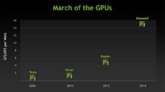
Those familiar with "Maxwell," codename for NVIDIA's next-generation GPU architecture, will find the new company roadmap posted below slightly different. For one, Maxwell is given a new launch timeframe, in 2014. Following this year's successful run at the markets with the Kepler family of GPUs, NVIDIA is looking up to Kepler Refresh GK11x family of GPUs to lead the company's product lineup in 2013. The new GPUs will arrive in the first half of next year, most likely in March, and will be succeeded by the Maxwell family of GPUs in 2014. Apart from the fact that Kepler established good performance and energy-efficiency leads over competitive architectures, a reason behind Maxwell's 2014 launch could be technical. We know from older reports that TSMC, NVIDIA's principal foundry partner, will begin mass production of 20 nanometer chips only by Q4-2013.
Source: WCCFTech
Add your own comment

20 Comments on NVIDIA to Pull Through 2013 with Kepler Refresh, "March of Maxwell" in 2014

#1
dj-electric
Always take what comes from WCCFTech with a spoon of salt. They have said a lot of speculation BS in the past that got proven wrong again and again. Probably for publicity of couse.
Posted on Reply
#2
mayankleoboy1
wccftech, WTF ?

TPU quoting from Wccftech ? :shadedshu
Wccftech is basically full of smelly brown stuff.
Posted on Reply
#3
eidairaman1
The Exiled Airman
sounds like someone was bored lol, 1/1048576s of a grain of salt
Posted on Reply
#4
bogami
2014

OO So far is this date. First they said, MAXWELL will come in 2013. Disappointment .:ohwell:
I wish AMD will make some very good GPU units to push closer to the date 2013. AMD 8870 Specs show promising increase, but the essence is 18u/m manufacturing technology. 16 times increase in GFLOPS per watt from may current GPU s sounds beautiful.:D
Posted on Reply
#9
Casecutter
Well a refresh of Kepler better mean something more than 192-Bit for the GTX660Ti and maybe even the GK106 GTX 660. Unless GDDR5 speeds are expected to jump and price for such are going to reduce, which I haven't heard anything either way.

Next I'd say Nvidia either needs to provide the GK106 a bunch more OC clocking within the Boost feature, or just drop Boost and give AIB’s the opening to supply it with VRM, voltage sections, and cooling to un-constraint them. As to what can be done with GK104, that's hard to ascertain, knowing they stretched it from mainstream part to enthusiast with clock and Boost they’ll either need to find more clock speed in process improvement or... ?
Posted on Reply
#11
the54thvoid
Super Intoxicated Moderator
Hmm...

The GK110 is the heart of the K20 Tesla piece. It's clocked at 705 MHz and draws 225(?)watts. It's the biggest chip (GK110) Nvidia have ever produced.

I'd very much like to see GK110 in a desktop part from a curiosity standpoint. Will they rip out compute again? If not, how much power will a higher clocked 7.1 billion transistor part draw? :eek:
Posted on Reply
#12
Benetanegia
the54thvoidHmm...

The GK110 is the heart of the K20 Tesla piece. It's clocked at 705 MHz and draws 225(?)watts. It's the biggest chip (GK110) Nvidia have ever produced.

I'd very much like to see GK110 in a desktop part from a curiosity standpoint. Will they rip out compute again? If not, how much power will a higher clocked 7.1 billion transistor part draw? :eek:
Well the Fermi GF110 based Tesla was clocked at 650 Mhz and had 250w TDP, while desktop part GTX 580 was clocked 772 Mhz and 244w TDP. Memory consumes a lot apparently (or any other explanation).

Going by that and the fact that Tesla K20x is clocked at 735 Mhz, IMO a 900 Mhz GTX780 might be possible or something close to that. Or maybe 850 Mhz for 225w TDP.
Posted on Reply
#13
Casecutter
Hum, As I said back a month ago... the question… "has TSMC got their process to the point that makes GK110 parts that are viable to gaming enthusiasts and not out of bounds on power. I think with geldings from Tesla and a more tailored second gen boost mapping this is saying they can, but I would say it not $550. Something tells me these will all be as GTX690’s, Nvidia only outing a singular design and construction as a factory release."

I'm thinking they have to run with a form of GK110 in this next spin, at least at first as a Limited Edition Nvidia Factory released card that AIB can dress up with decals (aka GTX690) then how much/many AIB’s will be permitted work their magic might be very curtailed. If Nvidia doesn't I can't see them finding enough of a bump in a GK114 re-spin to have it power a GTX780 and stay close to what a 8970 might bring with it. So we need to keep a close eye on what the Tesla release is pointing too.
Posted on Reply
#14
HumanSmoke
CasecutterI'm thinking they have to run with a form of GK110 in this next spin, at least at first as a Limited Edition Nvidia Factory released card that AIB can dress up with decals (aka GTX690) then how much/many AIB’s will be permitted work their magic might be very curtailed. If Nvidia doesn't I can't see them finding enough of a bump in a GK114 re-spin to have it power a GTX780 and stay close to what a 8970 might bring with it. So we need to keep a close eye on what the Tesla release is pointing too.
Depending on the order list for Tesla (which seems fairly deep), Quadro -which I'm pretty certain would follow, Nvidia still need to do something with the fully functional and high leakage GK110's. A limited run of GeForce boards seems the best return on investment- both from sales and PR. The card should sit midway between the GK114 and a dual-GK114 in performance, so should comfortably hold the top dog spot for a single GPU card...can't see Nvidia turning down that opportunity tbh, and being the halo product, they can tune core, memory and boost (if applicable) right up to the 300W PCI-SIG limit if need be- I doubt that the customer demographic would care too much. As Benetanegia noted, the K20X is a 235W board @ 732M core. Subtract 20-30W for culling 3GB of VRAM, add a little wattage for the extra SMX, and it should still allow for some considerable leeway.
Posted on Reply
#15
NC37
This could happen. AMD is stumbling once again. Not as bad as during the G92 era but still a little. If NV expects AMD to trip more I could see them riding Kepler longer.
Posted on Reply
#16
Casecutter
HumanSmokeNvidia still need to do something with the fully functional and high leakage GK110's
Any idea number of Tesla/Quarto GK110 that they figure they can sell into the HPC/professional market (which I have no clue). Based on the number of chips on wafer and yield there might a limited number for the consumer market. If 28Nm process is good a leakage is in check they’ll, as I said present A Halo product of limited numbers. Yields aren’t good the gaming world gets soaked, Nvidia will not leave them as scrap they'll spin them and supply all those with money, but not sense.
Posted on Reply
#17
HumanSmoke
CasecutterAny idea number of Tesla/Quarto GK110 that they figure they can sell into the HPC/professional market (which I have no clue).
Not sure really. Tesla will obviously be sharing billing with Xeon Phi from here on in. The Intel compile and programming is definitely going to eat into Nv's HPC share, no question about that. Numbers sold are anyones guess, a couple of hundred K20's (or similar from AMD/Intel) would be enough to make the Top500 list. There are also the hidden numbers- Xeon Phi lacks any TMU's, so any machine featuring them could also include a K20- The #7 in the Top500 (Stampede) which uses Xeon Phi also uses 128 K20's. An earlier estimate of units was 100,000-150,000, but that included Quadro K5000 and Tesla K10 GF104's.
The announced list:
Additional early customers include: Clemson University, Indiana University, Thomas Jefferson National Accelerator Facility (Jefferson Lab), King Abdullah University of Science and Technology (KAUST), National Center for Supercomputing Applications (NCSA), National Oceanic and Atmospheric Administration (NOAA), Oak Ridge National Laboratory (ORNL), University of Southern California (USC), and Shanghai Jiao Tong University (SJTU).
...as well as the usual vendor options (Seneca, AMAX, IBM, HP, SGI, Penguin, Silicon Mechanics, Asus etc.) - any user running Fermi based Tesla/CUDA would be an upgrade candidate I guess. For reliable numbers you'd have to cross-reference vendors contracts
CasecutterBased on the number of chips on wafer and yield there might a limited number for the consumer market. If 28Nm process is good a leakage is in check they’ll, as I said present A Halo product of limited numbers. Yields aren’t good the gaming world gets soaked, Nvidia will not leave them as scrap they'll spin them and supply all those with money, but not sense.
Anything above mainstream for gaming hasn't represented sense since GPU's were invented, hasn't stopped a decade plus of people shelling out of the latest and greatest.
I don't think GK110 was intended as a desktop GPU from the start, any usable SKU's Nvidia can parlay into cash and PR means they are playing with house money- even putting out a 1000 cards ensures that the longest bar/highest number on every graph on every review for a year or more has Nvidia's name on it. From a marketing standpoint Nvidia could sustain a loss on each card sold and it would still represent good business.
Posted on Reply
#18
NeoXF
i already know GF 700 will be based on the same architecture, nVidia already did that with GF 400 to 500 (albeit a fixed one), and GF 8000 up to GF 200 or so... Whatever comes after that, I don't care yet.

Tho I might be curious on what comes after AMD's Sea Islands/R8000s...
Posted on Reply
#19
Casecutter
HumanSmokeI don't think GK110 was intended as a desktop GPU from the start, any usable SKU's Nvidia can parlay into cash and PR means they are playing with house money- even putting out a 1000 cards ensures that the longest bar/highest number on every graph on every review for a year or more has Nvidia's name on it. From a marketing standpoint Nvidia could sustain a loss on each card sold and it would still represent good business.
Would very much agree, and why I think when "it is" released it will be built just as the GTX690 had been, a factory designed and built complete package that Nvidia will provide to AIB to add decals. I’d bet they already have designed, vetted, sitting the wings, awaiting final refinements before going to manufacturing. It preordained purpose, draw the lime-light away from AMD’s 8970 Southern Island release. But everything is pointing... from die size, efficacy, and price/perfrm it's not competitive part given given what we expect as the modern rationalization for what gaming GPU's should provide (may I say ghastlier than the GTX480 ever was :eek:). And, yes it will sell... ($600 IMO), it would still benefit Nvidia as their Halo, even if not making a profit... just a abhorrent PR boon. :ohwell:

So that sends me back to the mainstream GPU, (the real sweet spot of these second coming re-spins) as that's where either side will need to pull the loins' share. Within Nvidias' line-up would you sense the GTX660Ti and GTX660 will get condense under the GK116, with a Ti being bumped to a 256-Bit while the Non-Ti with 192-Bit? While tapering off wafer starts on the GK114 to be just say the GXT870Ti and then a Non-Ti?
Posted on Reply
#20
HumanSmoke
Casecutter... from die size, efficacy, and price/perfrm it's not competitive part given given what we expect as the modern rationalization for what gaming GPU's should provide (may I say ghastlier than the GTX480 ever was :eek:)
The people involved in the forum wars have already demonstrated that die size, efficiency, price/perf, and perf/mm^2 are moving targets. Cases in point being that Tahiti loses on three of those four points to GK104, and any argument usually ends up with one side invoking the "but Barts is better than GK104" apples-to-oranges argument. Likewise, when GF100/110 debuted, absolute performance at any cost and compute performance were the paramount considerations to Nvidians...not that that means diddly-squat to either AMD and Nvidia. Its the public at large and OEM's that determine sales, and I think we're both well aware of the relative abilities of each companies marketing and investment in brand awareness.
CasecutterSo that sends me back to the mainstream GPU, (the real sweet spot of these second coming re-spins) as that's where either side will need to pull the loins' share. Within Nvidias' line-up would you sense the GTX660Ti and GTX660 will get condense under the GK116, with a Ti being bumped to a 256-Bit while the Non-Ti with 192-Bit? While tapering off wafer starts on the GK114 to be just say the GXT870Ti and then a Non-Ti?
It's possible that the segmentation of SKU's moves closer to the GPU running the thing, but I think that having the second tier card (especially) moving to a different naming would be unlikely ( GTX 670 >> GTX 770Ti and GTX 660Ti >> GTX 770 ). Nvidia has shown reluctance in changing naming conventions at the top of the model line, unlike the high volume mainstream market. Having said that I feel that the plethora of GK104 derived models is in part due to the GK106 ramp being fairly late in the product cycle. A lot also depends on what AMD end up with. ~15% improvement for GK114/HD 8900 seems assured, but I'm not overly convinced the same can be said for Barts- mainly because AMD pretty much got Barts spot on the first time around.
You would also have to take into consideration that there could be a second 28nm refresh/model addition before 20nm debuts in mid-2014. I'm picking that both AMD and Nvidia have contingency plans in place just in case 20nm and the following 16nm FinFET processes slip.
Posted on Reply
Add your own comment
Jan 21st, 2025 07:31 EST change timezone

New Forum Posts

Popular Reviews

Controversial News Posts