News Posts matching #8 nm

Return to Keyword Browsing

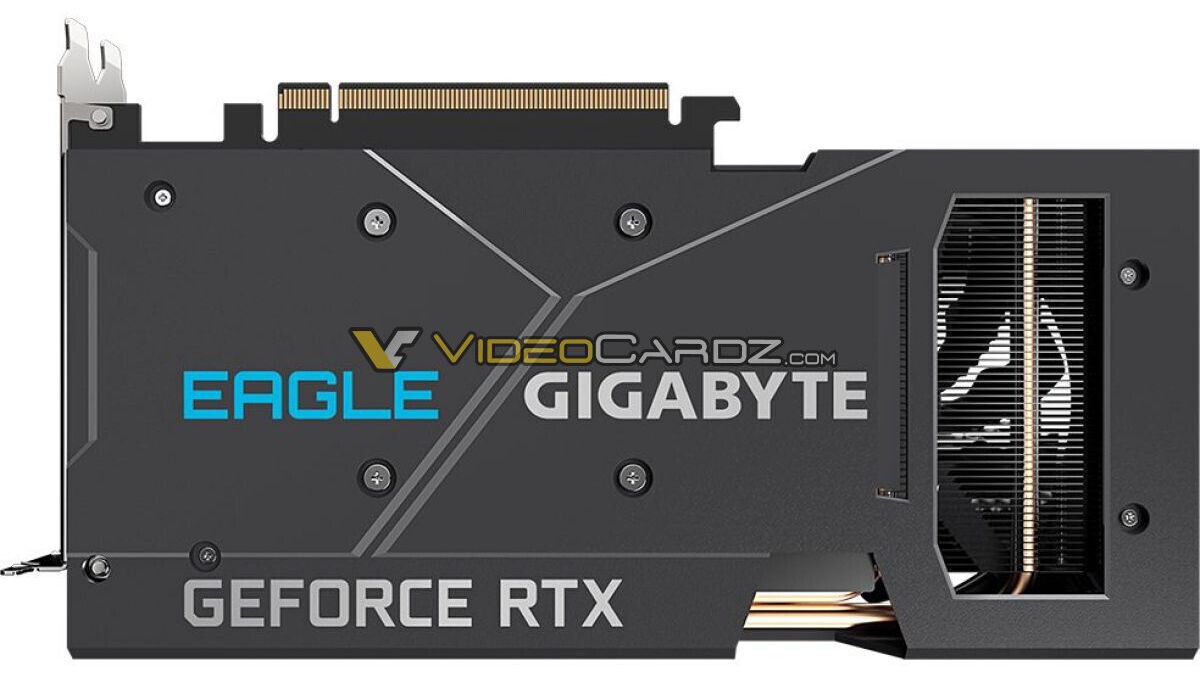
NVIDIA Announces GeForce RTX 3050 Ti Mobile and RTX 3050 Mobile

Alongside Intel's launch of the 11th Gen Core "Tiger Lake-H" desktop processor series, NVIDIA debuted its mid-range GeForce RTX 3050 Ti (mobile) and RTX 3050 (mobile) graphics processors. Both chips are designed with typical 3D power ranging between 35 W and 80 W. Both chips are based on the new 8 nm "GA107" silicon. This "Ampere" chip physically packs 2,560 CUDA cores across 20 streaming multiprocessors, with 80 tensor cores, 20 RT cores, and a 128-bit wide GDDR6 memory interface.

The GeForce RTX 3050 Ti (mobile) appears to be maxing out the GA107 silicon, featuring all 2,560 CUDA cores, 80 tensor cores, 20 RT cores, and 4 GB of GDDR6 memory across the chip's 128-bit wide memory bus. The RTX 3050 is slightly cut down, with 16 out of 20 SM enabled. This works out to 2,048 CUDA cores, 64 tensor cores, and 16 RT cores. The memory remains the same—4 GB GDDR6. Clock speeds will vary wildly depending on the notebook model, but typically, the RTX 3050 Ti can boost up to 1695 MHz, while the RTX 3050 can boost up to 1740 MHz. Both chips take advantage of PCI-Express 4.0 and Resizable BAR. The company didn't reveal memory clocks.

NVIDIA Earned $5 Billion During a GPU "Shortage" Quarter and Expects to Do it Again in the Next One

NVIDIA's recently published Q4-2020 + Fiscal Year 2021 results show that the alleged "GPU shortage" has had no bearing on the company's financials, with the company raking in $5 billion in revenue, in the quarter ending on January 31, 2021. In its outlook for the following quarter (Q1 FY 2022), the company expects to make another $5.30 billion (± 2%). To its credit, NVIDIA has been maintaining that the shortage of graphics cards in the retail market are a result of demand vastly outstripping supply; than a problem with the supply in and of itself (such as yields of the new 8 nm "Ampere" GPUs). The numbers show that NVIDIA's output of GPUs is fairly normal, and the problem lies with the retail supply-chain.

Crypto-currency mining and scalping are the two biggest problems affecting the availability of graphics cards in the retail market. Surging prices of crypto-currencies, coupled with the latest generation "Ampere" and RDNA2 graphics architectures having sufficient performance/Watt to mine crypto-currencies at viable scale, mean that crypto-miners are able to pick up inventory of graphics cards at wholesale; with very little making it down to retailers. Scalping is another major factor. Those with sophisticated online shopping tools are able to buy large quantities of graphics cards the moment they're available online, so they could re-sell or auction them at highly marked up prices, for profit. NVIDIA started to address the problem of miners by introducing measures that make their upcoming graphics cards artificially slower at mining, affecting the economics of using GPUs; while the problem of scalping remains at large.

AMD Reportedly in Plans to Outsource Partial Chip Production to Samsung

It's been doing the rounds in the rumor mill that AMD is looking to expand its semiconductor manufacturing partners beyond TSMC (for the 7 nm process and eventually 5 nm) and Global Foundries (12 nm process used in its I/O dies). The intention undoubtedly comes from the strain that's being placed on TSMC's production lines, as most foundry-less businesses outsource their wafer production to the Taiwanese companies' factories and manufacturing processes, which are currently the industry's best. However, as we've seen, TSMC is having a hard time scaling its production facilities to the unprecedented demand it's seeing from its consumers. The company also has recently announced it may prioritize new manufacturing capabilities for the automotive industry, which is also facing shortages in chips - and that certainly doesn't instill confidence in capacity increases for its non-automotive clients.

That's what originated form the rumor mill. Speculating, this could mean that AMD would be looking to outsource products with generally lower ASP to Samsung's foundries, instead of trying to cram even more silicon manufacturing onto TSMC's 7 nm process (where it already fabricates its Zen 3, RDNA 2, EPYC, and custom silicon solutions for latest-gen consoles). AMD might thus be planning on leveraging Samsung's 8 nm or even smaller fabrication processes as alternatives for, for example, lower-than-high-end graphics solutions and other product lines (such as APUs and FPGA production, should its acquisition of Xilinx come through).

NVIDIA, Samsung Strengthen Strategic Chip Fabrication Partnership in Deal

It seems NVIDIA and Samsung's partnership in bringing to life the green company's semiconductor designs isn't about to end anytime soon. Semiconductor analysts and insiders have said that NVIDIA and Samsung etched a new manufacturing deal on December 17th that still relates to the company's in-high-demand RTX-30 series graphics cards, which should see Samsung increase output - particularly at its Hwaseong plant - to sate the seemingly unquenchable demand from consumers and scalpers alike. The deal, which is roughly valued at "hundreds of billions won" will see Samsung double down on its 8 nm output for NVIDIA's latest gaming chips. This seems to put to rest speculation on an RTX 30-series redesign for TSMC's allegedly better 7 nm process - and according to the industry insiders, NVIDIA looked to Samsung specifically because of the need for "quick delivery of the chips".

This instills new life into Samsung's contract-based foundry business; according to market researcher TrendForce, Samsung's foundry business is expected to post a record $14.05 billion in sales this year, up 17.9% from 2019, as the company expands its client base not only through this and the previous NVIDIA deal, to Qualcomm Technologies Inc., Google, IBM, Cisco and China's Baidu. Samsung is accelerating its investment into EUV lithography in sub-7 nm processes so as to poach more customers and market share from industry behemoth and poster boy TSMC, spending 10 trillion won ($8.6 billion) to both improve technology and increase output on its foundries.

NVIDIA Announces the GeForce RTX 3060 Ti Graphics Card

NVIDIA today announced the GeForce RTX 3060 Ti, its new performance-segment graphics card that logically succeeds the GeForce RTX 2060 Super, at a starting MSRP of USD $399, with availability slated for December 2, 2020. The GPU is based on the same 8 nm "GA104" silicon as the $499 RTX 3070, but is heavily cut down, in featuring 38 out of 48 SMs (19 out of 24 TPCs), resulting in 4,864 CUDA cores, 152 Tensor cores, 38 RT cores, 152 TMUs, and 80 ROPs.

The RTX 3060 Ti is endowed with the same memory setup as the RTX 2060 Super—8 GB of 256-bit GDDR6 at 14 Gbps, yielding 448 GB/s bandwidth. NVIDIA developed a Founders Edition card based on the RTX 3060 Ti, which resembles the RTX 3070 Founders Edition with the exception of silvery metal replacing the gunmetal on the cooler frame. NVIDIA's various AIC partners have also announced their custom-design graphics cards. NVIDIA claims that the RTX 3060 Ti performs on par with the RTX 2080 Super, making it a beast for 1440p gaming with RTX-on. We put this claim to the test across our six launch-day reviews linked below.

Read the TechPowerUp reviews of NVIDIA RTX 3060 Ti Founders Edition, ASUS RTX 3060 Ti STRIX OC, Gigabyte RTX 3060 Ti Gaming OC Pro, MSI RTX 3060 Ti Gaming X Trio, Palit RTX 3060 Ti GamingPro OC, Zotac RTX 3060 Ti Twin Edge

Gigabyte RTX 3060 Ti EAGLE Graphics Cards Put on Display... By Bosnian Retailer

CPU Infotech, a Bosnian retailer of computer hardware, recently posted a photo of their latest inventory entries on Facebook. The photo showcased the newly/received Gigabyte RTX 3060 Ti EAGLE graphics cards, one of Gigabyte's designs for this particular SKU. The RTX 3060 Ti EAGLE features a dual-slot, dual-fan cooler design that's the smallest seen on any Ampere graphics card to date. The retailer announces that the inventory should be for sale pretty soon - and all publicly available information points towards a December 2nd release date for the RTX 3060 Ti.

The RTX 3060 Ti is supposed to beat NVIDIA's previous RTX 2080 SUPER graphics cards in performance, whilst costing half of that cards' launch asking price at $399. This should make this one of the most interesting performance-per-dollar graphics cards in NVIDIA's lineup. The RTX 3060 Ti is reportedly based on the same 8 nm "GA104" silicon as the RTX 3070, with further cuts. It features 38 out of the 48 available streaming multiprocessors on "GA104". This amounts to 4,864 "Ampere" CUDA cores, 152 tensor cores, and 38 "Ampere" RT cores. The memory configuration is unchanged from the RTX 3070, which translates to 8 GB of 14 Gbps GDDR6 memory across a 256-bit wide memory interface, with 448 GB/s of memory bandwidth. This marks the first time in years NVIDIA has launched a Ti model before the regular-numbered SKU in a given series, showcasing just how intense AMD competition is expected to be.

NVIDIA Reportedly Delays RTX 3060 Ti Launch to December

NVIDIA has reportedly delayed the launch of its GeForce RTX 3060 Ti performance-segment graphics card from mid-November to early-December, 2020. The RTX 3060 Ti is expected to be positioned a notch below the $500 RTX 3070, and based on the same 8 nm "GA104" silicon with 38 out of 48 streaming multiprocessors of the silicon enabled, amounting to 4,864 CUDA cores. The card is expected to come with the same exact memory setup as the RTX 3070, with 8 GB of 14 Gbps GDDR6 memory across a 256-bit wide bus. Besides a lighter core-configuration, the RTX 3060 Ti is expected to target a typical board power metric of 180 W, enabling designs with single 8-pin PCIe power connectors. Expreview, which broke the story on the launch delay predicts that the RTX 3060 Ti could perform similar to the RTX 2080 Super, a $700 high-end graphics card from the previous generation.

As for the delay, the RTX 3060 Ti was originally slated to be announced on November 17, but has its launch date pushed by two weeks, down to December 2. The reasons behind the delay could be anything from inventory building, to last-minute SKU optimization in the wake of AMD's Radeon RX 6000 series SKUs. Even the cheapest of the RX 6000-series SKUs announced so far, the RX 6800, is priced higher than the RTX 3070, and AMD claims higher performance than the RTX 2080 Ti (i.e. the card trades blows with the RTX 3070), which means the NVIDIA product stack could see many updates in the coming couple of months, some of which could even miss Holiday 2020 sales.

NVIDIA Readies New GeForce RTX 30-series SKU Positioned Between RTX 3070 and RTX 3080

Possibly unsure of the GeForce RTX 3070 tackling AMD's Radeon RX 6000 series parts, NVIDIA is designing a new RTX 30-series SKU positioned between the RTX 3070 and RTX 3080. This is not a 16 GB variant of the RTX 3070, but rather a new SKU based on the 8 nm "GA102" silicon, according to a reliable source with NVIDIA leaks, kopite7kimi. The SKU is based on the GA102 with the ASIC code "GA102-150-KD-A1." The silicon is configured with 7,424 CUDA cores across 58 streaming multiprocessors (29 TPCs), 232 tensor cores, 232 TMUs, 58 RT cores, and an unknown number of ROPs. According to kopite7kimi, the card is configured with a 320-bit wide memory interface, although it's not known if this is conventional GDDR6, like the RTX 3070 has, or faster GDDR6X, like that on the RTX 3080.

NVIDIA recently "cancelled" a future 16 GB variant of the RTX 3070, and 20 GB variant of the RTX 3080, which is possibly the company calibrating its response to the Radeon RX 6000 series. We theorize that doubling in memory amounts may not have hit the desired cost-performance targets; and the company probably believes the competitive outlook of the RTX 3080 10 GB is secure. This explains the need for a SKU with performance halfway between that of the RTX 3070 and RTX 3080. As for pricing, with the RTX 3070 positioned at $500 and the RTX 3080 at $700, the new SKU could be priced somewhere in between. AMD's RDNA2-based Radeon RX 6000 series GPUs are expected to feature DirectX 12 Ultimate logo compliance, meaning that there is a level playing ground between AMD and NVIDIA in the performance segment.

NVIDIA Reportedly Moving Ampere to 7 nm TSMC in 2021

A report straight from DigiTimes claims that NVIDIA is looking to upgrade their Ampere consumer GPUs from Samsung's 8 nm to TSMC's 7 nm. According to the source, the volume of this transition should be "very large", but most likely wouldn't reflect the entirety of Ampere's consumer-facing product stack. The report claims that TSMC has become more "friendly" to NVIDIA. This could be because TSMC now has available manufacturing capacity in 7 nm due to some of its clients moving to the company's 5 nm node, or simply because TSMC hadn't believed NVIDIA to consider Samsung as a viable foundry alternative - which it now does - and has thus lowered pricing.

There are various reasons being leveraged at this, none with substantial grounds other than "reported from industry sources". NVIDIA looking for better yields is one of the appointed reasons, as is its history as a TSMC customer. NVIDIA shouldn't have too high a cost porting its manufacturing to TSMC in terms of design changes to the silicon level so as to cater to different characteristics of TSMC's 7 nm, because the company's GA100 GPU (Ampere for the non-consumer market) is already manufactured at TSMC. The next part of this post is mere (relatively informed) speculation, so take that with a saltier disposition than what came before.

NVIDIA Unveils RTX A6000 "Ampere" Professional Graphics Card and A40 vGPU

NVIDIA today unveiled its RTX A6000 professional graphics card, the first professional visualization-segment product based on its "Ampere" graphics architecture. With this, the company appears to be deviating from the Quadro brand for the graphics card, while several software-side features retain the brand. The card is based on the same 8 nm "GA102" silicon as the GeForce RTX 3080, but configured differently. For starters, it gets a mammoth 48 GB of GDDR6 memory across the chip's 384-bit wide memory interface, along with ECC support.

The company did not reveal the GPU's CUDA core count, but mentioned that the card's typical board power is 300 W. The card also gets NVLink support, letting you pair up to two A6000 cards for explicit multi-GPU. It also supports GPU virtualization, including NVIDIA GRID, NVIDIA Quadro Virtual Data Center Workstation, and NVIDIA Virtual Compute Server. The card features a conventional lateral blower-type cooling solution, and its most fascinating aspect is its power input configuration, with just the one 8-pin EPS power input. We will update this story with more information as it trickles out.
Update 13:37 UTC: The company also unveiled the A40, a headless professional-visualization graphics card dedicated for virtual-GPU/cloud-GPU applications (deployments at scale in data-centers). The card has similar specs to the RTX A6000.

Update 13:42 UTC: NVIDIA website says that both the A40 and RTX A6000 a 4+4 pin EPS connector (and not 8-pin PCIe) for power input. An 8-pin EPS connector is capable of delivering up to 336 W (4x 7 A @ 12 V).

NVIDIA's Ampere-based Quadro RTX Graphics Card Pictured

Here is the first picture of an alleged next-generation Quadro RTX graphics card based on the "Ampere" architecture, courtesy YouTube channel "Moore's Law is Dead." The new Quadro RTX 6000-series shares many of its underpinnings with the recently launched GeForce RTX 3080 and RTX 3090, in being based on the 8 nm "GA102" silicon. The reference board design retains a lateral blower-type cooling solution, with the blower drawing in air from both sides of the card, through holes punched in the PCB, "Fermi" style. The card features the latest NVLink bridge connector, and unless we're mistaken, it features a single power input near its tail end, which is very likely a 12-pin Molex MicroFit 3.0 input.

As for specifications, "Moore's Law is Dead," shared a handful of alleged specifications that include maxing out of the "GA102" silicon, with all its 42 TPCs (84 SMs) enabled, working out to 10,752 CUDA cores. As detailed in an older story about the next-gen Quadro, NVIDIA is prioritizing memory size over bandwidth, which means this card will receive 48 GB of conventional 16 Gbps GDDR6 memory across the GPU's 384-bit wide memory interface. The 48 GB is achieved using twenty four 16 Gbit GDDR6 memory chips (two chips per 32-bit wide data-path). This configuration provides 768 GB/s of memory bandwidth, which is only 8 GB/s higher than that of the GeForce RTX 3080. The release date of the next-gen Quadro RTX will depend largely on the supply of 16 Gbit GDDR6 memory chips, with leading memory manufacturers expecting 2021 shipping, unless NVIDIA has secured an early production batch.

NVIDIA's Top "Ampere" Based Quadro RTX Features 10,752 CUDA Cores, 48GB Memory

Possible specifications of NVIDIA's next-generation flagship Quadro RTX professional graphics card leaked to the web. The SKU is possibly based on the same 8 nm "GA102" silicon as the GeForce RTX 3090, but features more of the silicon unlocked. It apparently features 10,752 CUDA cores, or exactly one TPC (two SMs) more than the RTX 3090. With 84 SM (42 TPC), the unnamed Quadro RTX should feature 84 RT cores, 336 Tensor cores, and 336 TMUs.

NVIDIA's choice for memory for the upcoming Quadro RTX flagship is interesting, as it's prioritizing memory size over bandwidth (which is more relevant in the professional visualization use-case dealing with large data sets). The card features 48 GB of conventional GDDR6 memory clocked at 16 Gbps over the chip's 384-bit wide memory interface, which should work out to 768 GB/s of memory bandwidth. The max GPU Boost frequency is pegged at 1860 MHz. There's no word on availability. Pictured below is the previous-gen Quadro RTX 5000.

NVIDIA GeForce RTX Ampere Chips Feature Three Binning Tiers, Mostly Good Dies are Present

Chip binning is a process of sorting out the manufactured silicon by quality. That means that each chip that comes from the silicon wafer is tested and sorted by different features. For example, a chip is tested for how much voltage it takes for operation, how cool it runs, and of course how it overclocks. By putting their chips through various testing, manufacturers often create binning tiers, where they can differentiate good and bad chips, so they know where to send, and if they should send the chips. The biggest and most complex approach for sending chips is for graphics cards. As there are different AIBs, manufacturers like NVIDIA and AMD need to send them chips of various qualities to incorporate in their products. It is a rather time-consuming and complex process to find out the bin type and the tier of chips, however today we are getting some information from Igor's Lab.

According to their sources, it is said that NVIDIA's latest GeForce RTX Ampere lineup features three binning tiers. There is "Bin 0" which represents an okay chip that can perform as intended, "Bin 1" chips which are good processors, and "Bin 2" processors which represent the best quality chips with the highest performance characteristics. These "Bin 2" dies run cooler compared to the rest and achieve higher overclocking speed. In reality, the binning represents coordination between the chip designer (NVIDIA in this case) and the manufacturer (Samsung with its 8N 8 nm process). It is said that from the complete pilot run of Ampere chips, Samsung ends up with 30% of the "Bin 0" dies, 60% of "Bin 1" dies, and only 10% of "Bin 2" dies. The production period was quite short and these numbers are good for Samsung, as they probably didn't have much time to work on it, so we can expect these numbers to improve.

Samsung Electronics Announces Second Quarter 2020 Results

Samsung Electronics reported today KRW 52.97 trillion in consolidated revenue and KRW 8.15 trillion in operating profit for the second quarter ended June 30, 2020. Even as the spread of COVID-19 caused closures and slowdowns at stores and production sites around the world, the Company responded to challenges through its extensive global supply chain, while minimizing the impact of the pandemic by strengthening online sales channels and optimizing costs.

Quarterly operating profit rose 26 percent from the previous quarter and 23 percent from a year earlier, thanks to firm demand for memory chips and appliances, as well as a one-off gain at its Display Panel Business. A partial recovery in global demand since May also helped offset some COVID-19 effects, resulting in higher earnings than initially expected. Revenue in the quarter fell 4 percent from the previous quarter and 6 percent from a year earlier due to reduced sales of smartphones and other devices.

NVIDIA GeForce "Ampere" GPUs Built on Samsung 8nm Instead of TSMC 7nm?

NVIDIA's upcoming GeForce "Ampere" family of GPUs will be built almost entirely on Samsung's 8 nanometer silicon fabrication process that's derived from its 10 nm node; rather than TSMC's 7 nm process, according to kopite7kimi, a source with a high hit-rate with NVIDIA rumors in the past. The 8LPP silicon fabrication node by Samsung is an extension of the company's 10LPP (10 nm) node. Both have the same fin pitch, but reductions are made in the areas of gate pitch (down by 6%) resulting in a transistor density of over 61 million/mm². Apparently NVIDIA's entire high-end product stack, including the GA102 silicon that powers at least three high-end consumer SKUs, are expected to be based on Samsung 8LPP.

NVIDIA GTX 1060 and GTX 1050 Successors in 2019; Turing Originally Intended for 10nm

NVIDIA could launch successors to its GeForce GTX 1060 series and GTX 1050 series only by 2019, according to a statement by an ASUS representative, speaking with PC Watch. This could mean that the high-end RTX 2080 Ti, RTX 2080, and RTX 2070, could be the only new SKUs for Holiday 2018 from NVIDIA, alongside cut-rate GeForce GTX 10-series SKUs. This could be a combination of swelling inventories of 10-series GPUs, and insufficient volumes of mid-range RTX 20-series chips, should NVIDIA even decide to extend real-time ray-tracing to mid-range graphics cards.

The way NVIDIA designed the RTX 2070 out of the physically smaller TU106 chip instead of TU104 leads us to believe that NVIDIA could carve out the GTX 1060-series successor based on this chip, since the RTX 2070 maxes it out, and NVIDIA needs to do something with imperfect chips. An even smaller chip (probably half-a-TU104?) could power the GTX 1050-series successor.

Samsung Completes Qualification of 8 nm LPP Process

Samsung Electronics announced today that their 8 nm FinFET process technology, 8LPP (Low Power Plus), has been qualified and is ready for production. Samsung's newest process node provides up to 10-percent lower power consumption with up to 10-percent area reduction from 10LPP through a narrower metal pitch. 8LPP is expected to provide benefits for applications including mobile, cryptocurrency and network/server. Samsung expects this 8 nm node to be the last feasible one with current fabrication technology - shown by the fact it's actually employing much of the same design and production processes and philosophy as the 10 nm node. Samsung is counting on EUV (Extreme Ultra Violet) technology to enable 7 nm and smaller process nodes.

"With the qualification completed three months ahead of schedule, we have commenced 8LPP production," said Ryan Lee, Vice President of Foundry Marketing at Samsung Electronics. "Samsung Foundry continues to expand its process portfolio in order to provide distinct competitive advantages and excellent manufacturability based on what our customers and the market require." Details of the recent update to Samsung's foundry roadmap, including 8LPP availability and 7nm EUV development, will be presented at the Samsung Foundry Forum Europe on October 18, 2017, in Munich, Germany.

Samsung Announces Comprehensive Process Roadmap Down to 4 nm

Samsung stands as a technology giant in the industry, with tendrils stretching out towards almost every conceivable area of consumer, prosumer, and professional markets. It is also one of the companies which can actually bring up the fight to Intel when it comes to semiconductor manufacturing, with some analysts predicting the South Korean will dethrone Intel as the top chipmaker in Q2 of this year. Samsung scales from hyper-scale data centers to the internet-of-things, and is set to lead the industry with 8nm, 7nm, 6nm, 5nm, 4nm and 18nm FD-SOI in its newest process technology roadmap. The new Samsung roadmap shows how committed the company is (and the industry with it) towards enabling the highest performance possible from the depleting potential of the silicon medium. The 4 nm "post FinFET" structure process is set to be in risk production by 2020.

This announcement also marks Samsung's reiteration on the usage of EUV (Extreme Ultra Violet) tech towards wafer manufacturing, a technology that has long been hailed as the savior of denser processes, but has been ultimately pushed out of market adoption due to its complexity. Kelvin Low, senior director of foundry marketing at Samsung, said that the "magic number" for productivity (as in, with a sustainable investment/return ratio) with EUV is 1,500 wafers per day. Samsung has already exceeded 1,000 wafers per day and has a high degree of confidence that 1,500 wafers per day is achievable.
Return to Keyword Browsing
Apr 22nd, 2025 19:51 CDT change timezone

New Forum Posts

Popular Reviews

Controversial News Posts