Monday, September 17th 2018

NVIDIA GTX 1060 and GTX 1050 Successors in 2019; Turing Originally Intended for 10nm

NVIDIA could launch successors to its GeForce GTX 1060 series and GTX 1050 series only by 2019, according to a statement by an ASUS representative, speaking with PC Watch. This could mean that the high-end RTX 2080 Ti, RTX 2080, and RTX 2070, could be the only new SKUs for Holiday 2018 from NVIDIA, alongside cut-rate GeForce GTX 10-series SKUs. This could be a combination of swelling inventories of 10-series GPUs, and insufficient volumes of mid-range RTX 20-series chips, should NVIDIA even decide to extend real-time ray-tracing to mid-range graphics cards.

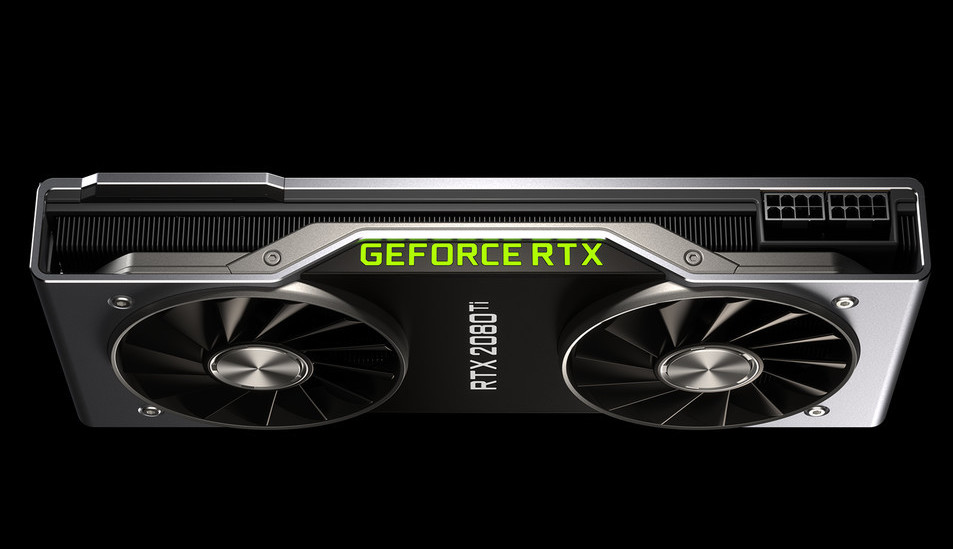
The way NVIDIA designed the RTX 2070 out of the physically smaller TU106 chip instead of TU104 leads us to believe that NVIDIA could carve out the GTX 1060-series successor based on this chip, since the RTX 2070 maxes it out, and NVIDIA needs to do something with imperfect chips. An even smaller chip (probably half-a-TU104?) could power the GTX 1050-series successor.
The PC Watch interview also states that NVIDIA's "Turing" architecture was originally designed for Samsung 10 nanometer silicon fabrication process, but was faced with delays and redesigning for the 12 nm process. This partially explains how NVIDIA hasn't kept up with the generational power-draw reduction curve of the previous 4 generations. NVIDIA has left the door open for a future optical-shrink of Turing to the 8 nm silicon fabrication node, an extension of Samsung's 10 nm node, with reduction in transistor sizes.
Sources: PC Watch, PCOnline.com.cn, Dylan on Reddit
Add your own comment

39 Comments on NVIDIA GTX 1060 and GTX 1050 Successors in 2019; Turing Originally Intended for 10nm

#1
Ferrum Master
And actually it will turn out that AMD still we be smartest of the bunch, ignoring nvidia and keeping up their development pace, keeping hand in hand with the time the smaller tech processes become mature.

I looking at this generation purely as beta test. Will pass it for sure, the TPU vote also shows that I am not the only one thinking like that. Arguing that mid tier cards won't get tensor cores? IMHO the flagships barely will manage to deliver proper FPS with the features enabled unless dumbed down.

No upgrades for this year, I guess.
Posted on Reply
#2
TheOne
I'm interested in seeing where they price the mid-range GPU's.
Posted on Reply
#3
NC37
106 series chips in the 70 series. Pretty bad. They must know AMD won't have decent competition for Turing so they can get away with that.
Posted on Reply
#4
renz496
Ferrum MasterAnd actually it will turn out that AMD still we be smartest of the bunch, ignoring nvidia and keeping up their development pace, keeping hand in hand with the time the smaller tech processes become mature.

I looking at this generation purely as beta test. Will pass it for sure, the TPU vote also shows that I am not the only one thinking like that. Arguing that mid tier cards won't get tensor cores? IMHO the flagships barely will manage to deliver proper FPS with the features enabled unless dumbed down.

No upgrades for this year, I guess.
Nvidia have to do that or they will not going to launch anything in 2018. Waiting for 7nm probably wise but consumer grade gpu based on 7nm probably will not be feasible until the end of 2019 or even 2020 anyway. Remember the big boys like Qualcomm and Apple going gobble up most of the capacity for cutting edge process.
Posted on Reply
#5
Upgrayedd
Are any of the new cards fully enabled or are they all cut or disabled or missing a memory chip?
Posted on Reply
#6
Vya Domus
NC37they must know AMD won't have decent competition for Turing so they can get away with that.
Nope, Nvidia shifted their silicon stack like this before as well back when they released Kepler.
Posted on Reply
#7
londiste
The choice Nvidia made might have been long-term strategy, not a short one.
All opinions (especially on price-performance) aside 20-series are faster than 10-series cards and will sell regardless of the high price.
At the same time they (and frankly, industry) want raytracing adoption in one form or another - DXR, Vulkan has RT extensions, Optix/ProRender and other proprietary APIs.
Lack of competition in normal rendering space allowed them to do this in the extreme way we see.

The inclusion of RT hardware was a pretty well-kept secret, or at least the extent of that hardware. Clearly developers got their hands on the cards very late. I would suspect that RTX 2080Ti delay is to allow at least some games developers to add RTX stuff (even if it is DLSS) to games to bolster the sales, not card shortage or anything else.

First generation of any new thing will suck. Next one will be better. And moving to 10nm or 7nm should give them a boost in performance as well even if everything remains the same.
Posted on Reply
#8
SDR82
UpgrayeddAre any of the new cards fully enabled or are they all cut or disabled or missing a memory chip?
Just the 2070 is fully enabled (so no 2070 Ti). The 2080 and 2080 Ti are cut down so that it can leave space for the 2080 Plus and the Titan X.
Posted on Reply
#9
Ferrum Master
renz496Qualcomm and Apple going gobble up most of the capacity for cutting edge process.
PC tech doesn't care for mobile tech nodes. Apples and oranges.

It will be a mess, just as with tessellation it was at start.
Posted on Reply
#10
Vayra86
Gotta love how conveniently Nvidia announces pre-orders and not three weeks later they have production issues, and curiously that only became known after the initial reception of RTX was... lukewarm at best and with old Pascal stock laying around.

How stupid do they think ppl are...
Posted on Reply
#11
Frick
Fishfaced Nincompoop
Vayra86Gotta love how conveniently Nvidia announces pre-orders and not three weeks later they have production issues, and curiously that only became known after the initial reception of RTX was... lukewarm at best and with old Pascal stock laying around.

How stupid do they think ppl are...
How do you know how the RTX reception will be when the NDA isn't lifted yet?
Posted on Reply
#12
Vya Domus
FrickHow do you know how the RTX reception will be when the NDA isn't lifted yet?
It's hilarious we even consider discussing what the "reception" will be like when all this RTX stuff is going to be virtually nonexistent at launch. I think BFV is the only game that's supposed to come out with day one RTX support and Shadow of the Tomb Raider will receive a patch "later on".

That will be the RTX reception for ya when the NDA lifts, basically nothing to even talk about.
Posted on Reply
#13
HTC
Vayra86Gotta love how conveniently Nvidia announces pre-orders and not three weeks later they have production issues, and curiously that only became known after the initial reception of RTX was... lukewarm at best and with old Pascal stock laying around.

How stupid do they think ppl are...
Very stupid ...

How else do you think people will "save money" by buying more of these cards?
Posted on Reply
#14
ppn
TU102 12nm 18600Mtr/754mm² ~25 Mtr/mm² . How small is this on 10nm - 300 mm² given that it will cut down to 256 bit bus instead of 384.

8nm ~65M transistors/mm² provides 18% improvement over 10nm 55Mtr/mm² .

Intels 10nm provides 100 Mtr/mm². GFX cards using that that node will debut in 2020. 14nm GFX is unlikely but who knows.

7nm TSMC is 100 Mtr/mm² too.

So the cards that we didn't get this time will get smaller next time. Pretty cool.
Posted on Reply
#15
jabbadap
Ferrum MasterAnd actually it will turn out that AMD still we be smartest of the bunch, ignoring nvidia and keeping up their development pace, keeping hand in hand with the time the smaller tech processes become mature.

I looking at this generation purely as beta test. Will pass it for sure, the TPU vote also shows that I am not the only one thinking like that. Arguing that mid tier cards won't get tensor cores? IMHO the flagships barely will manage to deliver proper FPS with the features enabled unless dumbed down.

No upgrades for this year, I guess.
Smartest and smartest, I'm sure Nvidia will make a ton of money with Turing albeit it's expensive and probably expensive to manufacturing too. One thing is sure though they don't have x86 CPU so they have to keep releasing new gpus, AMD has the fine cpu and consoles to keep their revenue in check. Which reminds me completely off topic digitalfoundry's unboxing of Subor Z+ ryzen+vega chinese console.
Posted on Reply
#16
SDR82
ppnTU102 12nm 18600Mtr/754mm² ~25 Mtr/mm² . How small is this on 10nm - 300 mm² given that it will cut down to 256 bit bus instead of 384.

8nm ~65M transistors/mm² provides 18% improvement over 10nm 55Mtr/mm² .

Intels 10nm provides 100 Mtr/mm². GFX cards using that that node will debut in 2020. 14nm GFX is unlikely but who knows.

7nm TSMC is 100 Mtr/mm² too.

So the cards that we didn't get this time will get smaller next time. Pretty cool.
Mega-transistor per squared millimeter (Mtr/mm²) - This should really become the new standard of measurement of transistor design going forward, as the traditional reference using "7nm" / "10nm" etc doesn't refer to any measured distance in transistor design anymore....people's nuts still drop off when the "nano-meters" (marketing hogwash) doesn't meet their expectations.
Posted on Reply
#17
Caring1
SDR82Mega-transistor per squared millimeter (Mtr/mm²) - This should really become the new standard of measurement of transistor design going forward, as the traditional reference using "7nm" / "10nm" etc doesn't refer to any measured distance in transistor design anymore....people's nuts still drop off when the "nano-meters" (marketing hogwash) doesn't meet their expectations.
Nanometer is a unit of length, not quantity.
Posted on Reply
#18
SDR82
Caring1Nanometer is a unit of length, not quantity.
I know. My point is is that the traditional measurement of transistor design using "7nm" or "10nm" is complete BS, this is due to the complexities is today's designs, they should rather use the density measurement (Mtr/mm²) . Try and find "10nm" anywhere in the transistor design (No, it's not the space between the transistors, neither is it the size of the transistor, not even close...)
Posted on Reply
#19
TheinsanegamerN
Caring1Nanometer is a unit of length, not quantity.
Parsect is a measure of distance, not time.
Posted on Reply
#20
londiste
SDR82I know. My point is is that the traditional measurement of transistor design using "7nm" or "10nm" is complete BS, this is due to the complexities is today's designs, they should rather use the density measurement (Mtr/mm²) . Try and find "10nm" anywhere in the transistor design (No, it's not the space between the transistors, neither is it the size of the transistor, not even close...)
It is exactly the complexities of the designs that make density an even worse measurement. Density is somewhat standardized around SRAM cells that may or may not reflect how dense logic or other type or memory of something else is. Coupled with things done for thermal and power management of the chips, density is secondary.
Posted on Reply
#21
efikkan
Ferrum MasterAnd actually it will turn out that AMD still we be smartest of the bunch, ignoring nvidia and keeping up their development pace, keeping hand in hand with the time the smaller tech processes become mature.
Yes, AMD is secretly winning by not even participating, holding back is all part of the "master plan"…
You do know that their upcoming Navi is another refinement of GCN, right?
ppnTU102 12nm 18600Mtr/754mm² ~25 Mtr/mm² . How small is this on 10nm - 300 mm² given that it will cut down to 256 bit bus instead of 384…
Node names are all marketing at this point. Intel 10 nm is denser than Samsung 10 nm.
Also, designs are usually not shrunk proportionally. Usually colder parts are shrunk more, hotter parts are hardly shrunk at all.
Posted on Reply
#22
SDR82
londisteIt is exactly the complexities of the designs that make density an even worse measurement. Density is somewhat standardized around SRAM cells that may or may not reflect how dense logic or other type or memory of something else is. Coupled with things done for thermal and power management of the chips, density is secondary.
So if measuring density is worse, do you suggest sticking with the traditional measurements ("10nm"...which is the measurement of exactly NOTHING in the design)? Or is there a third option?
Posted on Reply
#23
Ferrum Master
efikkanYes, AMD is secretly winning by not even participating, holding back is all part of the "master plan"…
You do know that their upcoming Navi is another refinement of GCN, right?
You have hard evidence on that, right?
Posted on Reply
#24
renz496
Ferrum MasterPC tech doesn't care for mobile tech nodes. Apples and oranges.

It will be a mess, just as with tessellation it was at start.
Yes in the past we have stuff like 28nm LP and 28nm HP. but i thought that no longer the case since TSMC failed to deliver 20nmHP? And my point about capacity still valid. Majority of TSMC revenue still coming from the so called "mobile tech process" so majority 7nm process capacity will be shifted towards mobile process. The only one really need that high performance process most likely only nvidia and AMD. and one reason TSMC failed on 20nmHP before because they end of most of their development focus for small low power chip like SoC. Nvidia most likely did not want to repeat what happen with 28nm. To push the performance further they have to ditch compute oriented design from maxwell. Nvidia end up relying on kepler for their compute solution for four years! Good thing for nvidia they have very solid ecosystem with their tesla. If not GK110/210 has been crushed by AMD Hawaii just looking at raw performance alone. There is no guarantee TSMC successor to 16nmFF will end up the way nvidia want it to be. Instead of betting their future on the uncertainties they create the road for their future themselves by investing on custom process for their architecture.
Posted on Reply
#25
Ferrum Master
renz496Yes in the past we have stuff like 28nm LP and 28nm HP. but i thought that no longer the case since TSMC failed to deliver 20nmHP? And my point about capacity still valid. Majority of TSMC revenue still coming from the so called "mobile tech process" so majority 7nm process capacity will be shifted towards mobile process. The only one really need that high performance process most likely only nvidia and AMD. and one reason TSMC failed on 20nmHP before because they end of most of their development focus for small low power chip like SoC. Nvidia most likely did not want to repeat what happen with 28nm. To push the performance further they have to ditch compute oriented design from maxwell. Nvidia end up relying on kepler for their compute solution for four years! Good thing for nvidia they have very solid ecosystem with their tesla. If not GK110/210 has been crushed by AMD Hawaii just looking at raw performance alone. There is no guarantee TSMC successor to 16nmFF will end up the way nvidia want it to be. Instead of betting their future on the uncertainties they create the road for their future themselves by investing on custom process for their architecture.
Rubbish, you simply cannot compare die sizes of such scale with minuscle mobile die sizes. They are different processes, goals and usages, lines and plants. They do not compete with each other.
Posted on Reply
Add your own comment
Jul 16th, 2024 10:09 EDT change timezone

New Forum Posts

Popular Reviews

Controversial News Posts