News Posts matching #10nm

Return to Keyword Browsing

SK Hynix Develops Industry's First 1c (10nm-class) DDR5 Memory

SK hynix announced today that it has developed the industry's first 16 Gb DDR5 built using its 1c node, the sixth generation of the 10 nm process. The success marks the beginning of the extreme scaling to the level closer to 10 nm in the memory process technology. The degree of difficulty to advance the shrinking process of the 10 nm-range DRAM technology has grown over generations, but SK hynix has become the first in the industry to overcome the technological limitations by raising the level of completion in design, thanks to its industry-leading technology of the 1b, the fifth generation of the 10 nm process.

SK hynix said it will be ready for mass production of the 1c DDR5 within the year to start volume shipment next year. In order to reduce potential errors stemming from the procedure of advancing the process and transfer the advantage of the 1b, which is widely applauded for its best performing DRAM, in the most efficient way, the company extended the platform of the 1b DRAM for development of 1c. The new product comes with an improvement in cost competitiveness, compared with the previous generation, by adopting a new material in certain process of the extreme ultraviolet, or EUV, while optimizing the EUV application process of total. SK hynix also enhanced productivity by more than 30% through technological innovation in design.

GIGABYTE Launches New G5/G7 Gaming Laptop

GIGABYTE TECHNOLOGY Co. Ltd, the global leading brand of PC, launches GIGABYTE Gaming G5/G7 gaming laptops equipped with 10nm Intel 12th Gen Processor today. A laptop to meet the wide range of needs in multitasking, gaming, and entertainment, with 12th Gen Intel Core i5-12500H laptop CPU, which is comprised of 12-core, 16 threads, and a maximum clock rate of 4.5GHz, to meet the needs for telecommuting and online classes, the purchase of high-performance laptops has been made easier with the adoption of Core i5-12500H, the Core i5 processor is powerful enough to effortlessly handle users' routines. Equipped with the graphics cards of NVIDIA GeForce RTX 30 Series, also introduces MUX switch graphics card switching technology, discrete GPU can be directly output to the display with just one click, which can easily improve the game performance and increase the frame rate in fierce game battles. For offering authentic gaming specifications and flexible expandability of hardware. The series can satisfy the user's needs for playing multiple roles in life.

Intel Rebadges 10nm Enhanced SuperFin Node as "Intel 7," Invents Other Creative Node Names

Intel, in a move comparable to its competitors' Performance Rating system from the 1990s, has invented a new naming scheme for its in-house foundry nodes to claim technological parity with contemporaries such as TSMC and Samsung, that are well into the sub-10 nm class. Back in the i586 era, when Intel's competitors such as AMD and Cyrix, couldn't keep up with its clock-speeds yet found their chips to be somewhat competitive, they invented the PR (processor rating) system, with a logical number attempting to denote parity with an Intel processor's clock-speed. For example, a PR400 processor rating meant that the chip rivaled a Pentium II 400 MHz (which it mostly didn't). The last that the PR system made sense was with the final generation of single-core performance chips, Pentium 4 and Athlon XP, beyond which, the introduction of multi-core obfuscated the PR system. A Phenom X4 9600 processor didn't mean performance on par with a rival Intel chip running at an impossible 9.60 GHz.

Intel's new foundry naming system sees its 10 nm Enhanced SuperFin node re-badge as "Intel 7." The company currently builds 11th Gen Core "Tiger Lake" processors on the 10 nm SuperFin node, and is expected to build its upcoming 12th Gen Core "Alder Lake" chips on its refinement, the 10 nm Enhanced SuperFin, which will now be referred to as "Intel 7." The company is careful to avoid using the nanometer unit next to the number, instead signaling the consumer that the node somehow offers transistor density and power characteristics comparable to a 7 nm node. Intel 7 offers a 10-15 percent performance/Watt gain over 10 nm SuperFin, and is already in volume production, with a debut within 2021 with "Alder Lake."

Intel Starts Production of 10nm Xeon Scalable Processors

Intel highlighted the company's focus on execution of core products and showcased the company's broader portfolio, in addition to sharing more on what's coming in the year ahead. As part of its disclosures, Intel announced the recent production of its 3rd Gen Intel Xeon Scalable processors (code-named "Ice Lake") with volume ramp taking place during the first quarter of 2021. Intel's 10 nm Xeon Scalable processors feature architectural and platform innovations that boost performance, security and operational efficiency within data centers.

"Today marks a significant milestone for Intel as we continue to accelerate the delivery of our 10 nm products and maintain an intense focus on delivering a predictable cadence of leadership products for our customers," said Navin Shenoy, executive vice president and general manager of the Data Platforms Group at Intel. "Our 3rd Gen Intel Xeon Scalable platform represents a strategic part of our data center strategy and one that we've created alongside some of our biggest customers to enable the data center of tomorrow."

Intel Expands 10nm Manufacturing Capacity

In response to incredible customer demand, Intel has doubled its combined 14 nm and 10 nm manufacturing capacity over the past few years. To do this, the company found innovative ways to deliver more output within existing capacity through yield improvement projects and significant investments in capacity expansion. This video recounts that journey, which even included re-purposing existing lab and office space for manufacturing.

"Over the last three years, we have doubled our wafer volume capacity, and that was a significant investment. Moving forward, we're not stopping… We are continuing to invest into factory capacity to ensure we can keep up with the growing needs of our customers," says Keyvan Esfarjani, senior vice president and general manager of Manufacturing and Operations at Intel. The company also ramped its new 10 nm process this year. Intel currently manufactures 10 nm products in high volumes at its Oregon and Arizona sites in the U.S. and its site in Israel.

Samsung Begins Mass Production of 16Gb LPDDR5 DRAM at World's Largest Semiconductor Line

Samsung Electronics, the world leader in advanced memory technology, today announced that its second production line in Pyeongtaek, Korea, has commenced mass production of the industry's first 16-gigabit (Gb) LPDDR5 mobile DRAM, using extreme ultraviolet (EUV) technology. Built on Samsung's third-generation 10 nm-class (1z) process, the new 16Gb LPDDR5 boasts the highest mobile memory performance and largest capacity to enable more consumers to enjoy the full benefits of 5G and AI features in next-generation smartphones.

"The 1z-based 16Gb LPDDR5 elevates the industry to a new threshold, overcoming a major developmental hurdle in DRAM scaling at advanced nodes," said Jung-bae Lee, executive vice president of DRAM Product & Technology at Samsung Electronics. "We will continue to expand our premium DRAM lineup and exceed customer demands, as we lead in growing the overall memory market."

Intel 10nm SuperFin Process Goes up Against TSMC 7nm

Intel on Thursday made several technological disclosures about its latest silicon fabrication process, the 10 nm SuperFin. With this, the company is changing the nomenclature of its node refinements, away from the ## nm++ naming scheme (with each "+" denoting a refinement, or internode), to a more descriptive naming scheme. The new 10 nm SuperFin node is the first refinement of the company's 10 nm node that debuted with the company's 10th Gen Core "Ice Lake" processors last year, and promises energy efficiency in the ballpark of 7 nm-class nodes by competitors TSMC and Samsung. While past generations of internodes (refinements) delivered energy efficiency improvements of around 3-5%, 10 nm SuperFin offers the kind of improvements expected from a brand new node, according to Intel.

The 10 nm SuperFin node is composed of two key innovations, the SuperMIM capacitor and a redesigned FinFET transistor. The new SuperMIM (metal insulator metal) capacitor offers a 5x increase in capacitance compared to devices in this class. The redesigned FinFET introduces a new barrier that reduces via resistance by 30%. Combined, the 10 nm SuperFin node affords chips a V/F curve comparable to a die-shrink to a whole new silicon fabrication node, without any change in transistor density. The first product built on 10 nm SuperFin is the upcoming Core "Tiger Lake" processor addressing the client-segment. The company is already working on enhancements of this node relevant for data-center processors.

Intel 10nm Product Lineup for 2020 Revealed: Alder Lake and Ice Lake Xeons

A leaked Intel internal slide surfaced on Chinese social networks, revealing five new products the company will build on its 10 nm silicon fabrication process. These include the "Alder Lake" heterogenous desktop processor, "Tiger Lake" mobile processor, "Ice Lake" based Xeon Scalable enterprise processors, DG1 discrete GPU, and "Snow Ridge" 5G base-station SoC. Some, if not all of these products, will implement Intel's new 10 nm+ silicon fabrication node that is expected to go live within 2020.

"Alder Lake" is a desktop processor that implements Intel's new heterogenous x86 core design that's making its debut with "Lakefield." The chip features up to 8 larger "Willow Cove" or "Golden Cove" CPU cores, and up to 8 smaller "Tremont" or "Gracemont" cores. This 8-big/8-small combo lets the chip achieve TDP targets around 80 Watts. Next up is "Tiger Lake," Intel's next-generation mobile processor family succeeding "Ice Lake." This microarchitecture implements "Willow Cove" CPU cores in a homogeneous setup, alongside Xe architecture based integrated graphics. "Ice Lake-SP" is Intel's next enterprise architecture that places mature "Sunny Cove" CPU cores in extreme core-count dies. Lastly, there's "Snow Ridge," an SoC purpose built for 5G base-stations. Image quality notwithstanding, these slides don't appear particularly new, and it's likely that COVID-19 has destabilized the roadmap. For instance, "Alder Lake," and "Ice Lake-SP" are expected to be 10 nm++ chips, a node that doesn't go live before 2021.

Where's the Ryzen Effect? Intel posts Record Financials

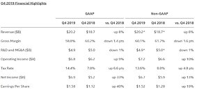
Intel Corporation today reported fourth-quarter and full-year 2019 financial results. The company also announced that its board of directors approved a five percent cash dividend increase to $1.32 per share on an annual basis. The board declared a quarterly dividend of $0.33 per share on the company's common stock, which will be payable on March 1 to shareholders of record on February 7.

"In 2019, we gained share in an expanded addressable market that demands more performance to process, move and store data," said Bob Swan, Intel CEO. "One year into our long-term financial plan, we have outperformed our revenue and EPS expectations. Looking ahead, we are investing to win the technology inflections of the future, play a bigger role in the success of our customers and increase shareholder returns."

Intel CFO Talks About 7nm Rollout, Delay in 10nm, Increased Competition from AMD

Intel CFO George Davis in an interview with Barron's commented on the company's financial health, and some of the reasons behind its rather conservative gross margin guidance looking forward to at least 2023. Intel's current product stack is moving on to the company's 10 nm silicon fabrication process in a phased manner. The company is allocating 10 nm to mobile processors and enterprise processors, while brazening it out with 14 nm on the client-desktop and HEDT platforms until they can build 10 nm desktop parts. AMD has deployed its high-IPC "Zen 2" microarchitecture on TSMC's 7 nm DUV process, with plans to go EUV in the coming months.

"We're still keenly focused on gross margin. Everything from capital efficiency to the way we're designing our products. What we've said though, the delay in 10 nanometer means that we're going to be a little bit disadvantaged on unit cost for a period of time. We actually gave guidance for gross margin out in 2021 to help people understand. 2023 is the period that we were ultimately guiding [when] we're going to see very strong revenue growth and margin expansion. We've got to get through this period where we have the 10 nanometer being a little bit late [as] we're not optimized on a node that we're on. But [by] then we're moving to a two to two and a half year cadence on the next nodes. So we're pulling in the spending on 7 nanometer, which will start up in the second half of 2021 because we think it's the right thing to do competitively," he said.

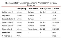
Intel Scraps 10nm for Desktop, Brazen it Out with 14nm Skylake Till 2022?

In a shocking piece of news, Intel has reportedly scrapped plans to launch its 10 nm "Ice Lake" microarchitecture on the client desktop platform. The company will confine its 10 nm microarchitectures, "Ice Lake" and "Tiger Lake" to only the mobile platform, while the desktop platform will see derivatives of "Skylake" hold Intel's fort under the year 2022! Intel gambles that with HyperThreading enabled across the board and increased clock-speeds, it can restore competitiveness with AMD's 7 nm "Zen 2" Ryzen processors with its "Comet Lake" silicon that offers core-counts of up to 10.

"Comet Lake" will be succeeded in 2021 by the 14 nm "Rocket Lake" silicon, which somehow combines a Gen12 iGPU with "Skylake" derived CPU cores, and possibly increased core-counts and clock speeds over "Comet Lake." It's only 2022 that Intel will ship out a truly new microarchitecture on the desktop platform, with "Meteor Lake." This chip will be built on Intel's swanky 7 nm EUV silicon fabrication node, and possibly integrate CPU cores more advanced than even "Willow Cove," possibly "Golden Cove."

Microsoft Unveils First Intel "Lakefield" Device and Surface Lineup with 10th Gen Core

Today, at a launch event in New York City, Microsoft previewed the Surface Neo, a category-defining device co-engineered with Intel. The dual-screen device will be powered by Intel's unique processor, code-named "Lakefield," that features an industry-first architecture combining a hybrid CPU with Intel's Foveros 3D packaging technology. It offers device-makers more flexibility to innovate on design, form factor and experience.

"The innovation we've achieved with Lakefield gives our industry partners the ability to deliver on new experiences, and Microsoft's Neo is trailblazing a new category of devices. Intel is committed to pushing the boundaries of computing by delivering key technology innovations for partners across the ecosystem," said Gregory Bryant, Intel executive vice president and general manager of the Client Computing Group.

Intel Ships First 10nm Agilex FPGAs

Intel today announced that it has begun shipments of the first Intel Agilex field programmable gate arrays (FPGAs) to early access program customers. Participants in the early access program include Colorado Engineering Inc., Mantaro Networks, Microsoft and Silicom. These customers are using Agilex FPGAs to develop advanced solutions for networking, 5G and accelerated data analytics.

"The Intel Agilex FPGA product family leverages the breadth of Intel innovation and technology leadership, including architecture, packaging, process technology, developer tools and a fast path to power reduction with eASIC technology. These unmatched assets enable new levels of heterogeneous computing, system integration and processor connectivity and will be the first 10nm FPGA to provide cache-coherent and low latency connectivity to Intel Xeon processors with the upcoming Compute Express Link," said Dan McNamara, Intel senior vice president and general manager of the Networking and Custom Logic Group.

Intel Expands 10th Gen Intel Core Mobile Processor Family

Today, Intel introduced eight additional 10th Gen Intel Core processors for modern laptop computing. The new mobile PC processors (formerly code-named "Comet Lake") are tailor-made to deliver increased productivity and performance scaling for demanding, multi-threaded workloads while still enabling thin-and-light laptop and 2 in 1 designs with uncompromising battery life. These processors are performance powerhouses that bring double digit performance gains compared with the previous generation. The lineup also includes Intel's first 6-core processor in the U-series, faster CPU frequencies, faster memory interfaces and the industry redefining connectivity with Intel Wi-Fi 6 (Gig+) and broader scaling of Thunderbolt 3. More than 90 additional designs based on the 10th Gen Intel Core processor family will hit the shelves for the holiday season.

"Our 10th Gen Intel Core mobile processors provide customers with the industry-leading range of products that deliver the best balance of performance, features, power and design for their specific needs. From multitasking to everyday content creation, the newest additions to the family scale performance for even higher levels of productivity -- in addition to offering best-in-class platform connectivity via Wi-Fi 6 (Gig+) and Thunderbolt 3 that people expect with 10th Gen," said Chris Walker, Intel corporate vice president and general manager of Mobility Client Platforms in the Client Computing Group.

Intel Starts Shipping 10 nm Ice Lake CPUs to OEMs

During its second quarter earnings call, Intel announced that it has started shipping of 10th generation "Core" CPUs to OEMs. Making use of 10 nm lithography, the 10th generation of "Core" CPUs, codenamed Ice Lake, were qualified by OEMs earlier in 2019 in order to be integrated into future products. Ice Lake is on track for holiday season 2019, meaning that we can expect products on-shelves by the end of this year. That is exciting news as the 10th generation of Core CPUs is bringing some exciting micro-architectural improvements along with the long awaited and delayed Intel's 10nm manufacturing process node.

The new CPUs are supposed to get around 18% IPC improvement on average when looking at direct comparison to previous generation of Intel CPUs, while being clocked at same frequency. This time, even regular mobile/desktop parts will get AVX512 support, alongside VNNI and Cryptography ISA extensions that are supposed to bring additional security and performance for the ever increasing number of tasks, especially new ones like Neural Network processing. Core configurations will be ranging from dual core i3 to quad core i7, where we will see total of 11 models available.

Intel's CEO Blames 10 nm Delay on being "Too Aggressive"

During Fortune's Brainstorm Tech conference in Aspen, Colorado, Intel's CEO Bob Swan took stage and talked about the company, about where Intel is now and where they are headed in the future and how the company plans to evolve. Particular focus was put on how Intel became "data centric" from "PC centric," and the struggles it encountered.

However, when asked about the demise of Moore's Law, Swan detailed the aggressiveness that they approached the challenge with. Instead of the regular two times improvement in transistor density every two years, Swan said that Intel has always targeted better and greater densities so that it would stay the leader in the business.

Intel "Sapphire Rapids" Brings PCIe Gen 5 and DDR5 to the Data-Center

As if the mother of all ironies, prior to its effective death-sentence dealt by the U.S. Department of Commerce, Huawei's server business developed an ambitious product roadmap for its Fusion Server family, aligning with Intel's enterprise processor roadmap. It describes in great detail the key features of these processors, such as core-counts, platform, and I/O. The "Sapphire Rapids" processor will introduce the biggest I/O advancements in close to a decade, when it releases sometime in 2021.

With an unannounced CPU core-count, the "Sapphire Rapids-SP" processor will introduce DDR5 memory support to the data-center, which aims to double bandwidth and memory capacity over the DDR4 generation. The processor features an 8-channel (512-bit wide) DDR5 memory interface. The second major I/O introduction is PCI-Express gen 5.0, which not only doubles bandwidth over gen 4.0 to 32 Gbps per lane, but also comes with a constellation of data-center-relevant features that Intel is pushing out in advance as part of the CXL Interconnect. CXL and PCIe gen 5 are practically identical.

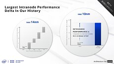
Intel Switches Gears to 7nm Post 10nm, First Node Live in 2021

Intel's semiconductor manufacturing business has had a terrible past 5 years as it struggled to execute its 10 nanometer roadmap forcing the company's processor designers to re-hash the "Skylake" microarchitecture for 5 generations of Core processors, including the upcoming "Comet Lake." Its truly next-generation microarchitecture, codenamed "Ice Lake," which features a new CPU core design called "Sunny Cove," comes out toward the end of 2019, with desktop rollouts expected 2020. It turns out that the 10 nm process it's designed for, will have a rather short reign at Intel's fabs. Speaking at an investor's summit on Wednesday, Intel put out its silicon fabrication roadmap that sees an accelerated roll-out of Intel's own 7 nm process.

When it goes live and fit for mass production some time in 2021, Intel's 7 nm process will be a staggering 3 years behind TSMC, which fired up its 7 nm node in 2018. AMD is already mass-producing CPUs and GPUs on this node. Unlike TSMC, Intel will implement EUV (extreme ultraviolet) lithography straightaway. TSMC began 7 nm with DUV (deep ultraviolet) in 2018, and its EUV node went live in March. Samsung's 7 nm EUV node went up last October. Intel's roadmap doesn't show a leap from its current 10 nm node to 7 nm EUV, though. Intel will refine the 10 nm node to squeeze out energy-efficiency, with a refreshed 10 nm+ node that goes live some time in 2020.

Intel 10nm Ice Lake to Quantitatively Debut Within 2019

Intel put out interesting details about its upcoming 10 nanometer "Ice Lake" CPU microarchitecture rollout in its recent quarterly financial results call. The company has started qualification of its 10 nm "Ice Lake" processors. This involves sending engineering samples to OEMs, system integrators and other relevant industry partners, and getting the chips approved for their future product designs. The first implementation of "Ice Lake" will not be a desktop processor, but rather a low-power mobile SoC designed for ultraportables, codenamed "Ice Lake-U." This SoC packs a 4-core/8-thread CPU based on the "Sunny Cove" core design, and Gen11 GT2 integrated graphics with 64 execution units and nearly 1 TFLOP/s compute power. This SoC will also support WiFi 6 and LPDDR4X memory.

Intel CEO Bob Swan also remarked that the company has doubled its 10 nm yield expectations. "On the [10 nm] process technology front, our teams executed well in Q1 and our velocity is increasing," he said, adding "We remain on track to have volume client systems on shelves for the holiday selling season. And over the past four months, the organization drove a nearly 2X improvement in the rate at which 10nm products move through our factories." Intel is prioritizing enterprise over desktop, as "Ice Lake-U" will be followed by "Ice Lake-SP" Xeon rollout in 2020. There was no mention of desktop implementations such as "Ice Lake-S." Intel is rumored to be preparing a stopgap microarchitecture for the desktop platform to compete with AMD "Matisse" Zen 2 AM4 processors, codenamed "Comet Lake." This is essentially a Skylake 10-core die fabbed on existing 14 nm++ node. AMD in its CES keynote announced an achievement of per-core performance parity with Intel, so it could be interesting to see how Intel hopes 10 "Skylake" cores match up to 12-16 "Zen 2" cores.

Intel Reports First-Quarter 2019 Financial Results

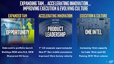
Intel Corporation today reported first-quarter 2019 financial results. "Results for the first quarter were slightly higher than our January expectations. We shipped a strong mix of high performance products and continued spending discipline while ramping 10nm and managing a challenging NAND pricing environment. Looking ahead, we're taking a more cautious view of the year, although we expect market conditions to improve in the second half," said Bob Swan, Intel CEO. "Our team is focused on expanding our market opportunity, accelerating our innovation and improving execution while evolving our culture. We aim to capitalize on key technology inflections that set us up to play a larger role in our customers' success, while improving returns for our owners."

In the first quarter, the company generated approximately $5.0 billion in cash from operations, paid dividends of $1.4 billion and used $2.5 billion to repurchase 49 million shares of stock. In the first quarter, Intel achieved 4 percent growth in the PC-centric business while data-centric revenue declined 5 percent.

Intel Driving Data-Centric World with New 10nm Intel Agilex FPGA Family

Intel announced today a brand-new product family, the Intel Agilex FPGA. This new family of field programmable gate arrays (FPGA) will provide customized solutions to address the unique data-centric business challenges across embedded, network and data center markets. "The race to solve data-centric problems requires agile and flexible solutions that can move, store and process data efficiently. Intel Agilex FPGAs deliver customized connectivity and acceleration while delivering much needed improvements in performance and power for diverse workloads," said Dan McNamara, Intel senior vice president, Programmable Solutions Group.

Customers need solutions that can aggregate and process increasing amounts of data traffic to enable transformative applications in emerging, data-driven industries like edge computing, networking and cloud. Whether it's through edge analytics for low-latency processing, virtualized network functions to improve performance, or data center acceleration for greater efficiency, Intel Agilex FPGAs are built to deliver customized solutions for applications from the edge to the cloud. Advances in artificial intelligence (AI) analytics at the edge, network and the cloud are compelling hardware systems to cope with evolving standards, support varying AI workloads, and integrate multiple functions. Intel Agilex FPGAs provide the flexibility and agility required to meet these challenges and deliver gains in performance and power.

Intel Announces Broadest Product Portfolio for Moving, Storing, and Processing Data

Intel Tuesday unveiled a new portfolio of data-centric solutions consisting of 2nd-Generation Intel Xeon Scalable processors, Intel Optane DC memory and storage solutions, and software and platform technologies optimized to help its customers extract more value from their data. Intel's latest data center solutions target a wide range of use cases within cloud computing, network infrastructure and intelligent edge applications, and support high-growth workloads, including AI and 5G.

Building on more than 20 years of world-class data center platforms and deep customer collaboration, Intel's data center solutions target server, network, storage, internet of things (IoT) applications and workstations. The portfolio of products advances Intel's data-centric strategy to pursue a massive $300 billion data-driven market opportunity.

Samsung Develops Industry's First 3rd-generation 10nm-Class DRAM

Samsung Electronics Co., Ltd., the world leader in advanced memory technology, today announced that it has developed a 3rd-generation 10-nanometer-class (1z-nm) eight-gigabit (Gb) Double Data Rate 4 (DDR4) DRAM for the first time in the industry. In just 16 months since it began mass producing the 2nd-generation 10nm-class (1y-nm) 8Gb DDR4, development of 1z-nm 8Gb DDR4 without the use of Extreme Ultra-Violet (EUV) processing has pushed the limits of DRAM scaling even further.

As 1z-nm becomes the industry's smallest memory process node, Samsung is now primed to respond to increasing market demands with its new DDR4 DRAM that has more than 20-percent higher manufacturing productivity compared to the previous 1y-nm version. Mass production of the 1z-nm 8Gb DDR4 will begin within the second half of this year to accommodate next-generation enterprise servers and high-end PCs expected to be launched in 2020.

Samsung Launches Highest-capacity Mobile DRAM

Samsung Electronics Co., Ltd., the world leader in advanced memory technology, today announced that it has begun mass producing the highest-capacity mobile DRAM - the industry's first 12-gigabyte (GB) low-power double data rate 4X (LPDDR4X) package - optimized for tomorrow's premium smartphones. Featuring higher capacity than most ultra-thin notebooks, the new mobile DRAM will enable smartphone users to take full advantage of all the features in next-generation smartphones.

"With mass production of the new LPDDR4X, Samsung is now providing a comprehensive lineup of advanced memory to power the new era of smartphones, from 12GB mobile DRAM to 512GB eUFS 3.0 storage," said Sewon Chun, executive vice president of Memory Marketing at Samsung Electronics. "Moreover, with the LPDDR4X, we're strengthening our position as the premium mobile memory maker best positioned to accommodate rapidly growing demand from global smartphone manufacturers."

Intel 10nm "Ice Lake" to Combine "Sunny Cove" CPU Cores with Gen11 iGPU

Intel's upcoming "Ice Lake" die could be the company's biggest processor innovation in a decade, combining new clean-slate design "Sunny Cove" CPU cores, and a new integrated graphics solution based on the company's Gen11 architecture. "Sunny Cove" introduces significant IPC (single-thread performance) gains over "Coffee Lake," introduces new ISA instruction sets, including AVX-512; and a brand new uncore component; while the Gen11 graphics core is Intel's first iGPU to reach the 1 TFLOP/s mark. Intel demonstrated the ultra-low power "Ice Lake-U" SoC platform in its 2018 Architecture Day briefing.

This "Ice Lake-U" chip, with its TDP in the ballpark of 15 W, was shown ripping through 7-zip and "Tekken 7." With 7-zip, Intel was trying to demonstrate vector-AES and SHA-NI improving archive encryption performance by 75 percent over "Skylake." The Gen11 iGPU was shown providing a smoother gameplay than Skylake with Gen9, although the company neither mentioned resolution, nor frame-rates. Anandtech wagers it's above 30 fps.
Return to Keyword Browsing
Dec 20th, 2024 00:55 EST change timezone

New Forum Posts

Popular Reviews

Controversial News Posts