Apr 7th, 2025 00:22 EDT
change timezone
Latest GPU Drivers
New Forum Posts
- Stock PSU with Razer Core X with adapter to 12VHPWR (1)
- 9070XT or 7900XT (43)
- Possible to stream your nintendo switch to discord ? (0)
- No idea how many watts this USB-C port will supply? (5)
- What's your latest tech purchase? (23487)
- gpu heirarchy/performance/benchmarks- whos lying? (39)
- Share your AIDA 64 cache and memory benchmark here (3049)
- I dont think the HT-Omega sound card company has anyone running it anymore. Cant get responses from customer service for last 2 years. (2)
- A dozen drivers for HD4670, and which do I choose? (10)
- Clicks & Pops in Mic Audio due to buffer underruns. Please send help. (3)
Popular Reviews
- ASUS Prime X870-P Wi-Fi Review
- UPERFECT UStation Delta Max Review - Two Screens In One
- PowerColor Radeon RX 9070 Hellhound Review
- Upcoming Hardware Launches 2025 (Updated Apr 2025)
- Corsair RM750x Shift 750 W Review
- Sapphire Radeon RX 9070 XT Pulse Review
- Sapphire Radeon RX 9070 XT Nitro+ Review - Beating NVIDIA
- DDR5 CUDIMM Explained & Benched - The New Memory Standard
- AMD Ryzen 7 9800X3D Review - The Best Gaming Processor
- AMD Ryzen 9 9950X3D Review - Great for Gaming and Productivity
Controversial News Posts
- MSI Doesn't Plan Radeon RX 9000 Series GPUs, Skips AMD RDNA 4 Generation Entirely (146)
- NVIDIA GeForce RTX 5060 Ti 16 GB SKU Likely Launching at $499, According to Supply Chain Leak (140)
- Microsoft Introduces Copilot for Gaming (124)
- AMD Radeon RX 9070 XT Reportedly Outperforms RTX 5080 Through Undervolting (119)
- NVIDIA Reportedly Prepares GeForce RTX 5060 and RTX 5060 Ti Unveil Tomorrow (115)
- Over 200,000 Sold Radeon RX 9070 and RX 9070 XT GPUs? AMD Says No Number was Given (100)
- NVIDIA GeForce RTX 5050, RTX 5060, and RTX 5060 Ti Specifications Leak (97)
- Nintendo Switch 2 Launches June 5 at $449.99 with New Hardware and Games (92)
News Posts matching #Aldebaran
Return to Keyword Browsing
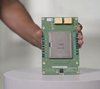
AMD Releases its CDNA2 MI250X "Aldebaran" HPC GPU Block Diagram
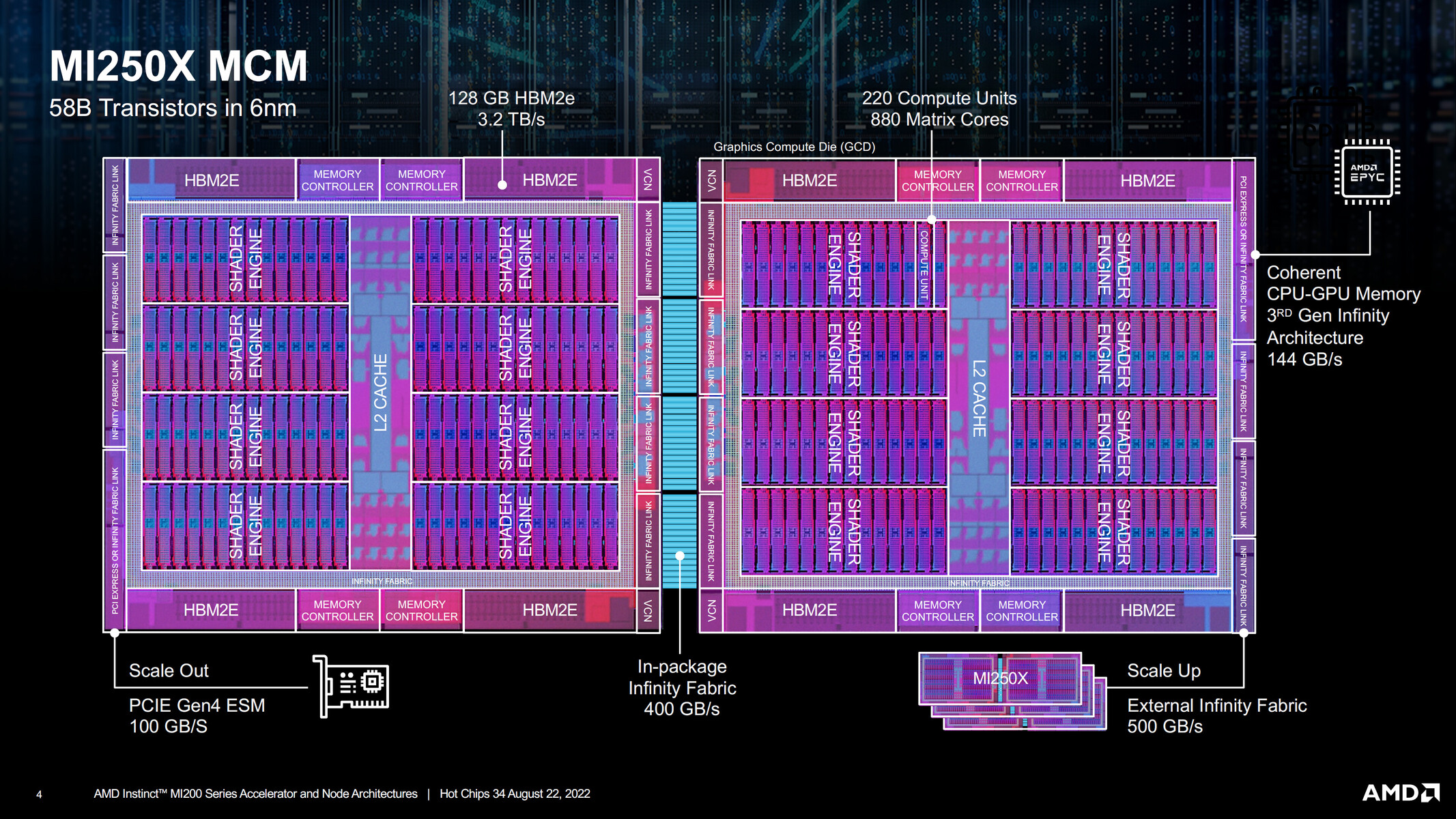
AMD in its HotChips 22 presentation released a block-diagram of its biggest AI-HPC processor, the Instinct MI250X. Based on the CDNA2 compute architecture, at the heart of the MI250X is the "Aldebaran" MCM (multi-chip module). This MCM contains two logic dies (GPU dies), and eight HBM2E stacks, four per GPU die. The two GPU dies are connected by a 400 GB/s Infinity Fabric link. They each have up to 500 GB/s of external Infinity Fabric bandwidth for inter-socket communications; and PCI-Express 4.0 x16 as the host system bus for AIC form-factors. The two GPU dies together make up 58 billion transistors, and are fabricated on the TSMC N6 (6 nm) node.
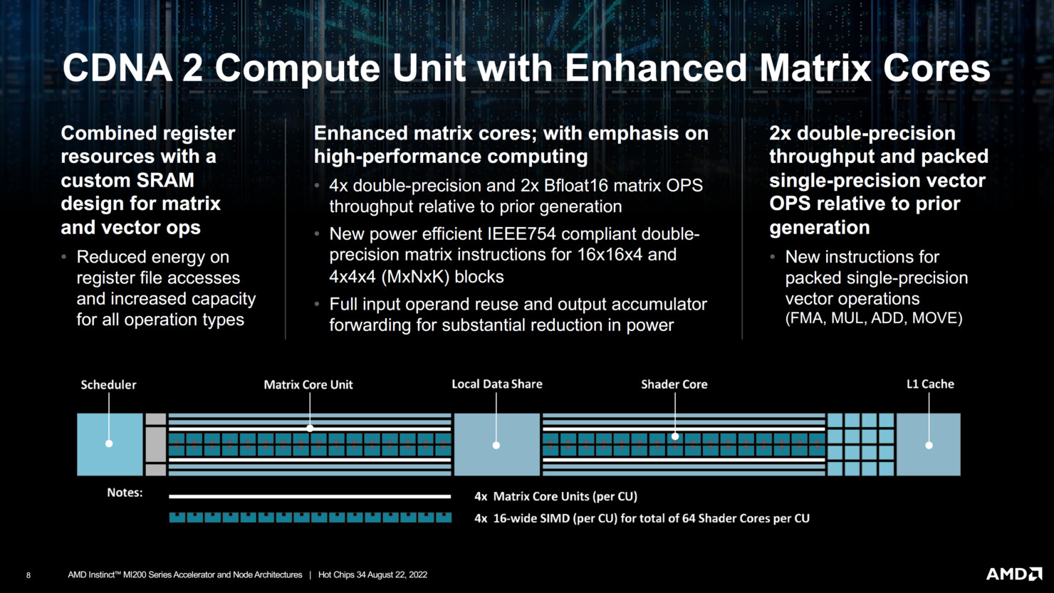
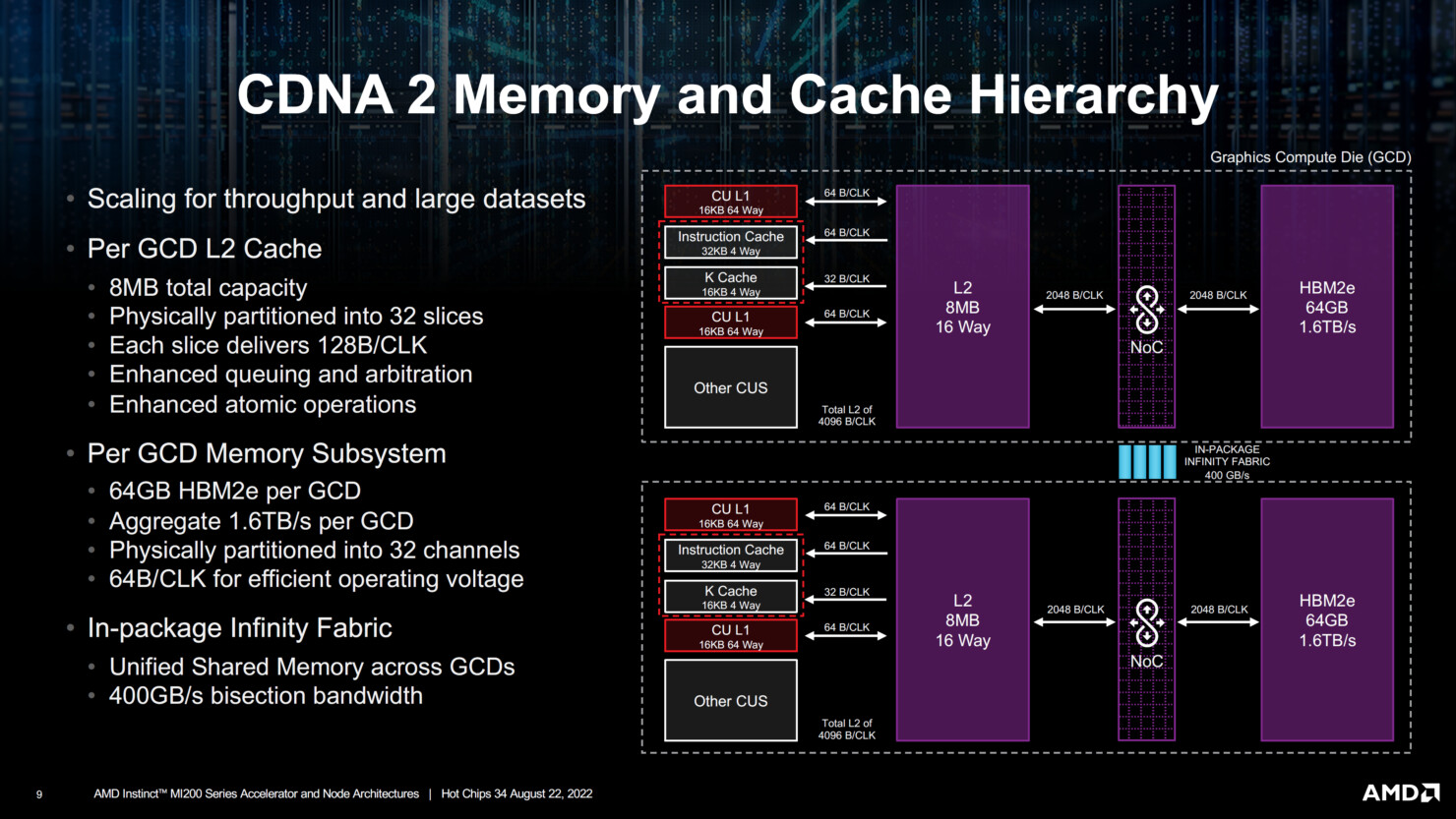
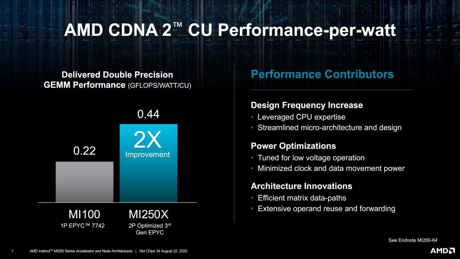
The component hierarchy of each GPU die sees eight Shader Engines share a last-level L2 cache. The eight Shader Engines total 112 Compute Units, or 14 CU per engine. The CDNA2 compute unit contains 64 stream processors making up the Shader Core, and four Matrix Core Units. These are specialized hardware for matrix/tensor math operations. There are hence 7,168 stream processors per GPU die, and 14,336 per package. AMD claims a 100% increase in double-precision compute performance over CDNA (MI100). AMD attributes this to increases in frequencies, efficient data paths, extensive operand reuse and forwarding; and power-optimization enabling those higher clocks. The MI200 is already powering the Frontier supercomputer, and is working for more design wins in the HPC space. The company also dropped a major hint that the MI300, based on CDNA3, will be an APU. It will incorporate GPU dies, core-logic, and CPU CCDs onto a single package, in what is a rival solution to NVIDIA Grace Hopper Superchip.


The component hierarchy of each GPU die sees eight Shader Engines share a last-level L2 cache. The eight Shader Engines total 112 Compute Units, or 14 CU per engine. The CDNA2 compute unit contains 64 stream processors making up the Shader Core, and four Matrix Core Units. These are specialized hardware for matrix/tensor math operations. There are hence 7,168 stream processors per GPU die, and 14,336 per package. AMD claims a 100% increase in double-precision compute performance over CDNA (MI100). AMD attributes this to increases in frequencies, efficient data paths, extensive operand reuse and forwarding; and power-optimization enabling those higher clocks. The MI200 is already powering the Frontier supercomputer, and is working for more design wins in the HPC space. The company also dropped a major hint that the MI300, based on CDNA3, will be an APU. It will incorporate GPU dies, core-logic, and CPU CCDs onto a single package, in what is a rival solution to NVIDIA Grace Hopper Superchip.
AMD Readies MI250X Compute Accelerator with 110 CUs and 128 GB HBM2E
AMD is preparing an update to its compute accelerator lineup with the new MI250X. Based on the CDNA2 architecture, and built on existing 7 nm node, the MI250X will be accompanied by a more affordable variant, the MI250. According to leaks put out by ExecutableFix, the MI250X packs a whopping 110 compute units (7,040 stream processors), running at 1.70 GHz. The package features 128 GB of HBM2E memory, and a package TDP of 500 W. As for speculative performance numbers, it is expected to offer double-precision (FP64) throughput of 47.9 TFLOP/s, ditto full-precision (FP32), and 383 TFLOP/s half-precision (FP16 and BFLOAT16). AMD's MI200 "Aldebaran" family of compute accelerators are expected to square off against Intel's "Ponte Vecchio" Xe-HPC, and NVIDIA Hopper H100 accelerators in 2022.


Intel Ponte Vecchio Early Silicon Puts Out 45 TFLOPs FP32 at 1.37 GHz, Already Beats NVIDIA A100 and AMD MI100
Intel in its 2021 Architecture Day presentation put out fine technical details of its Xe HPC Ponte Vecchio accelerator, including some [very] preliminary performance claims for its current A0-silicon-based prototype. The prototype operates at 1.37 GHz, but achieves out at least 45 TFLOPs of FP32 throughput. We calculated the clock speed based on simple math. Intel obtained the 45 TFLOPs number on a machine running a single Ponte Vecchio OAM (single MCM with two stacks), and a Xeon "Sapphire Rapids" CPU. 45 TFLOPs sees the processor already beat the advertised 19.5 TFLOPs of the NVIDIA "Ampere" A100 Tensor Core 40 GB processor. AMD isn't faring any better, with its production Instinct MI100 processor only offering 23.1 TFLOPs FP32.


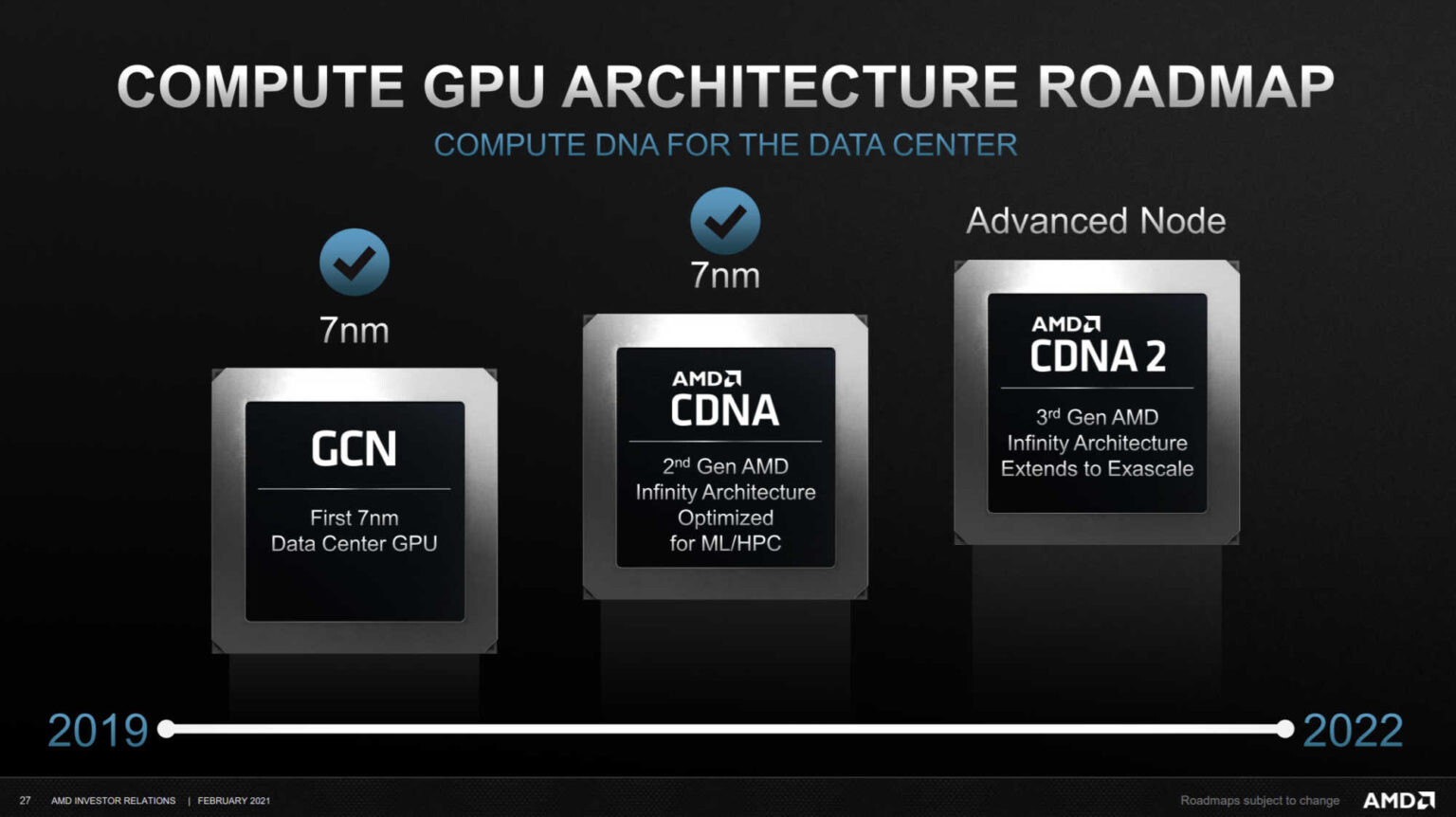
AMD Zen 4 and RDNA3 Confirmed for 2022, Zen 3 Refresh
AMD CEO Dr Lisa Su, in the company's Q2-2021 financial results call, confirmed that the company is on-track to launch the Zen 4 CPU microarchitecture and RDNA3 graphics architecture, in 2022. Zen 4 would herald the first major desktop platform change since the original Zen architecture, with the introduction of a new CPU socket, and support for DDR5 memory. The RDNA3 graphics architecture, meanwhile, is expected to nearly triple SIMD resources over the previous generation, and introduce even more fixed-function hardware for raytracing.
In the meantime, AMD is preparing a counter to Intel's 12th Gen Core "Alder Lake-S" processor, in the form of Zen 3 with 3D Vertical Cache, which is also being referred to as the Zen 3+ architecture. These processors feature additional last-level cache, and the company claims a 15% gaming performance uplift, which should help it close the gaming performance gap with Intel, and win on sheer core-count of its big cores. It remains to be seen if Zen 3+ remains on Socket AM4 or if it debuts AM5, as AMD will be under pressure to match "Alder Lake" in platform I/O, which includes DDR5. Dr Su also confirmed that AMD has started shipping the Instinct MI200 "Aldebaran" compute accelerator based on the CDNA2 architecture. AMD's first MCM GPU with two logic dies, "Aldebaran" takes the fight to NVIDIA's top A100 series compute accelerators, and has already scored wins with ongoing HPC/supercomputing projects.
In the meantime, AMD is preparing a counter to Intel's 12th Gen Core "Alder Lake-S" processor, in the form of Zen 3 with 3D Vertical Cache, which is also being referred to as the Zen 3+ architecture. These processors feature additional last-level cache, and the company claims a 15% gaming performance uplift, which should help it close the gaming performance gap with Intel, and win on sheer core-count of its big cores. It remains to be seen if Zen 3+ remains on Socket AM4 or if it debuts AM5, as AMD will be under pressure to match "Alder Lake" in platform I/O, which includes DDR5. Dr Su also confirmed that AMD has started shipping the Instinct MI200 "Aldebaran" compute accelerator based on the CDNA2 architecture. AMD's first MCM GPU with two logic dies, "Aldebaran" takes the fight to NVIDIA's top A100 series compute accelerators, and has already scored wins with ongoing HPC/supercomputing projects.
AMD MI200 "Aldebaran" Memory Size of 128GB Per Package Confirmed
The 128 GB per package memory size of AMD's upcoming Instinct MI200 HPC accelerator was confirmed, in a document released by Pawsey SuperComputing Centre, a Perth, Australia-based supercomputing firm that's popular with mineral prospecting companies located there. The company is currently working on Setonix, a 50-petaFLOP supercomputer being put together by HP Enterprise, which combines over 750 next-generation "Aldebaran" GPUs (referenced only as "AMD MI-Next GPUs"); and over 200,000 AMD EPYC "Milan" processor cores (the actual processor package count would be lower, and depend on the various core configs the builder is using).
The Pawsey document mentions 128 GB as the per-GPU memory. This corresponds with the rumored per-package memory of "Aldebaran." Recently imagined by Locuza_, an enthusiast who specializes in annotation of logic silicon dies, "Aldebaran" is a multi-chip module of two logic dies and eight HBM2E stacks. Each of the two logic dies, or chiplets, has 8,192 CDNA2 stream processors that add up to 16,384 on the package; and each of the two dies is wired to four HBM2E stacks over a 4096-bit memory bus. These are 128 Gbit (16 GB) stacks, so we have 64 GB memory per logic die, and 128 GB on the package. Find other drool worthy specs of the Pawsey Setonix in the screengrab below.
The Pawsey document mentions 128 GB as the per-GPU memory. This corresponds with the rumored per-package memory of "Aldebaran." Recently imagined by Locuza_, an enthusiast who specializes in annotation of logic silicon dies, "Aldebaran" is a multi-chip module of two logic dies and eight HBM2E stacks. Each of the two logic dies, or chiplets, has 8,192 CDNA2 stream processors that add up to 16,384 on the package; and each of the two dies is wired to four HBM2E stacks over a 4096-bit memory bus. These are 128 Gbit (16 GB) stacks, so we have 64 GB memory per logic die, and 128 GB on the package. Find other drool worthy specs of the Pawsey Setonix in the screengrab below.

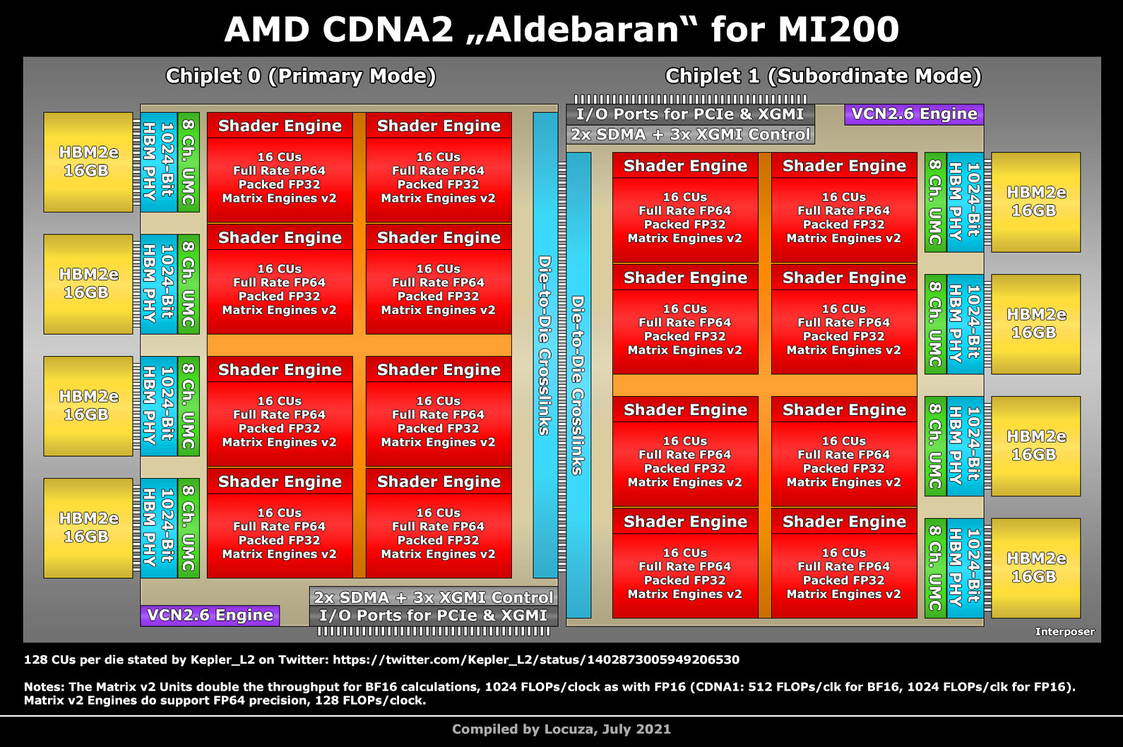
AMD CDNA2 "Aldebaran" MI200 HPC Accelerator with 256 CU (16,384 cores) Imagined
AMD Instinct MI200 will be an important product for the company in the HPC and AI supercomputing market. It debuts the CDNA2 compute architecture, and is based on a multi-chip module (MCM) codenamed "Aldebaran." PC enthusiast Locuza, who conjures highly detailed architecture based on public information, imagined what "Aldebaran" could look like. The MCM contains two logic dies, and eight HBM2E stacks. Each of the two dies has a 4096-bit HBM2E interface, which talks to 64 GB of memory (128 GB per package). A silicon interposer provides microscopic wiring among the ten dies.
Each of the two logic dies, or chiplets, has sixteen shader engines that have 16 compute units (CU), each. The CDNA2 compute unit is capable of full-rate FP64, packed FP32 math, and Matrix Engines V2 (fixed function hardware for matrix multiplication, accelerating DNN building, training, and AI inference). With 128 CUs per chiplet, assuming the CDNA2 CU has 64 stream processors, one arrives at 8,192 SP. Two such dies add up to a whopping 16,384, more than three times that of the "Navi 21" RDNA2 silicon. Each die further features its independent PCIe interface, and XGMI (AMD's rival to CXL), an interconnect designed for high-density HPC scenarios. A rudimentary VCN (Video CoreNext) component is also present. It's important to note here, that the CDNA2 CU, as well as the "Aldebaran" MCM itself, doesn't have a dual-use as a GPU, since it lacks much of the hardware needed for graphics processing. The MI200 is expected to launch later this year.
Each of the two logic dies, or chiplets, has sixteen shader engines that have 16 compute units (CU), each. The CDNA2 compute unit is capable of full-rate FP64, packed FP32 math, and Matrix Engines V2 (fixed function hardware for matrix multiplication, accelerating DNN building, training, and AI inference). With 128 CUs per chiplet, assuming the CDNA2 CU has 64 stream processors, one arrives at 8,192 SP. Two such dies add up to a whopping 16,384, more than three times that of the "Navi 21" RDNA2 silicon. Each die further features its independent PCIe interface, and XGMI (AMD's rival to CXL), an interconnect designed for high-density HPC scenarios. A rudimentary VCN (Video CoreNext) component is also present. It's important to note here, that the CDNA2 CU, as well as the "Aldebaran" MCM itself, doesn't have a dual-use as a GPU, since it lacks much of the hardware needed for graphics processing. The MI200 is expected to launch later this year.
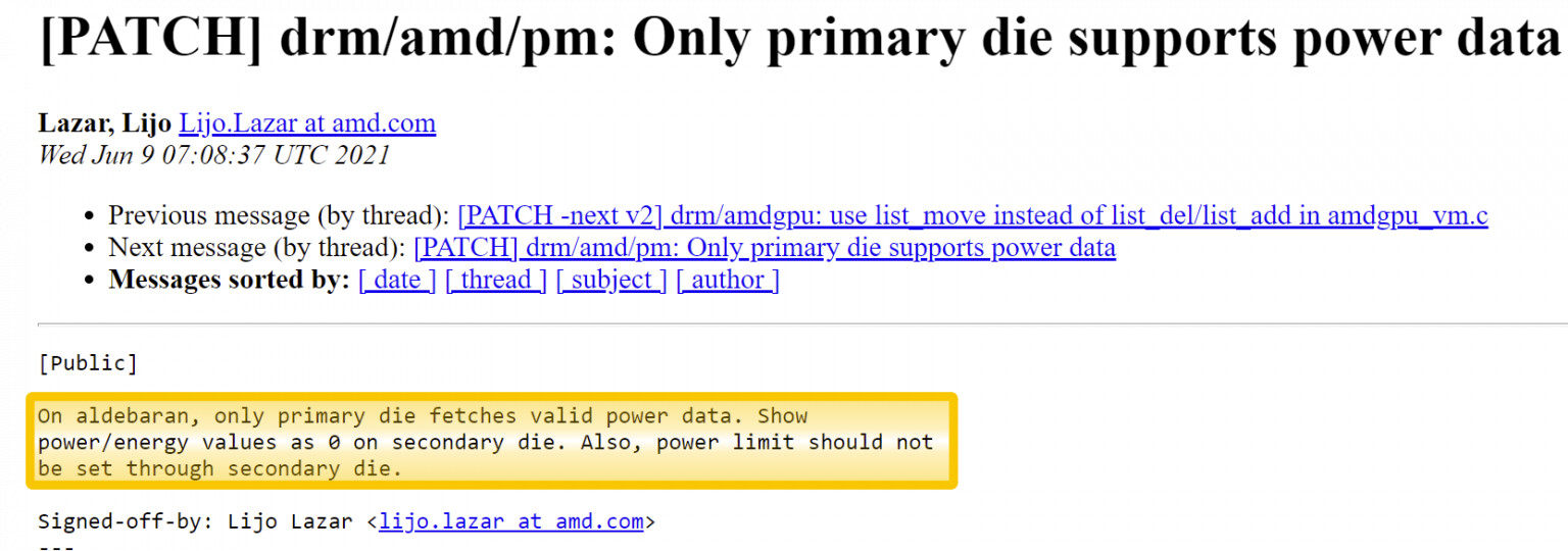
AMD Confirms CDNA2 Instinct MI200 GPU Will Feature at Least Two Dies in MCM Design
Today we've got the first genuine piece of information that confirms AMD's MCM approach to CDNA2, the next-gen compute architecture meant for ML/HPC/Exascale computing. This comes courtesy of a Linux kernel update, where AMD engineers annotated the latest Linux kernel patch with some considerations specific for their upcoming Aldebaran, CDNA2-based compute cards. Namely, the engineers clarify the existence of a "Die0" and a "Die1", where power data fetching should be allocated to Die0 of the accelerator card - and that the power limit shouldn't be set on the secondary die.
This confirms that Aldebaran will be made of at least two CDNA2 compute dies, and as (almost) always in computing, one seems to be tasked with general administration of both compute dies. It is unclear as of yet whether the HBM2 memory controller will be allocated to the primary die, or if there will be an external I/O die (much like in Zen) that AMD can leverage for off-chip communication. AMD's approach to CDNA2 will eventually find its way (in an updated form) for AMD's consumer-geared next-generation graphics architecture with RDNA3.

This confirms that Aldebaran will be made of at least two CDNA2 compute dies, and as (almost) always in computing, one seems to be tasked with general administration of both compute dies. It is unclear as of yet whether the HBM2 memory controller will be allocated to the primary die, or if there will be an external I/O die (much like in Zen) that AMD can leverage for off-chip communication. AMD's approach to CDNA2 will eventually find its way (in an updated form) for AMD's consumer-geared next-generation graphics architecture with RDNA3.
Apr 7th, 2025 00:22 EDT
change timezone
Latest GPU Drivers
New Forum Posts
- Stock PSU with Razer Core X with adapter to 12VHPWR (1)
- 9070XT or 7900XT (43)
- Possible to stream your nintendo switch to discord ? (0)
- No idea how many watts this USB-C port will supply? (5)
- What's your latest tech purchase? (23487)
- gpu heirarchy/performance/benchmarks- whos lying? (39)
- Share your AIDA 64 cache and memory benchmark here (3049)
- I dont think the HT-Omega sound card company has anyone running it anymore. Cant get responses from customer service for last 2 years. (2)
- A dozen drivers for HD4670, and which do I choose? (10)
- Clicks & Pops in Mic Audio due to buffer underruns. Please send help. (3)
Popular Reviews
- ASUS Prime X870-P Wi-Fi Review
- UPERFECT UStation Delta Max Review - Two Screens In One
- PowerColor Radeon RX 9070 Hellhound Review
- Upcoming Hardware Launches 2025 (Updated Apr 2025)
- Corsair RM750x Shift 750 W Review
- Sapphire Radeon RX 9070 XT Pulse Review
- Sapphire Radeon RX 9070 XT Nitro+ Review - Beating NVIDIA
- DDR5 CUDIMM Explained & Benched - The New Memory Standard
- AMD Ryzen 7 9800X3D Review - The Best Gaming Processor
- AMD Ryzen 9 9950X3D Review - Great for Gaming and Productivity
Controversial News Posts
- MSI Doesn't Plan Radeon RX 9000 Series GPUs, Skips AMD RDNA 4 Generation Entirely (146)
- NVIDIA GeForce RTX 5060 Ti 16 GB SKU Likely Launching at $499, According to Supply Chain Leak (140)
- Microsoft Introduces Copilot for Gaming (124)
- AMD Radeon RX 9070 XT Reportedly Outperforms RTX 5080 Through Undervolting (119)
- NVIDIA Reportedly Prepares GeForce RTX 5060 and RTX 5060 Ti Unveil Tomorrow (115)
- Over 200,000 Sold Radeon RX 9070 and RX 9070 XT GPUs? AMD Says No Number was Given (100)
- NVIDIA GeForce RTX 5050, RTX 5060, and RTX 5060 Ti Specifications Leak (97)
- Nintendo Switch 2 Launches June 5 at $449.99 with New Hardware and Games (92)