News Posts matching #GTX 260

Return to Keyword Browsing

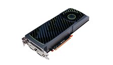
Revised GF110-based GTX 560 Ti On The Way: a GTX 570 In Disguise?

Those on a budget looking to upgrade their graphics cards might do well to wait a little while, NVIDIA is preparing an upgraded GTX 560 Ti. The current model is based on the GF114 GPU which has 384 CUDA cores, 32 TMUs, a 256-bit memory interface and 1GB VRAM. However, the new model discards the GF114 GPU and replaces it with the beefier GF110 GPU that's used on the GTX 570 & GTX 580 cards. As one would expect, this GPU will be cut down compared to its bigger brothers, featuring 448 CUDA cores, 56 TMUs, a 320-bit memory bus and likely 1280MB VRAM. Another improvement comes in the form of two SLI connectors, allowing 3-card setups to be built, but the cost compared to using more powerful cards must of course be considered before such a build is attempted. The new card will be called the "GTX 560 Ti (448 Core)", which follows a similar convention that was used with the GTX 260 when NVIDIA upgraded it to the GTX 260 (216 Core). Given that the memory bus and memory size are now the same as that of the GTX 570, it brings with it the intriguing possibility that such cards may be unlocked to full GTX 570 performance by enterprising enthusiasts who are not afraid of risking their warranty in their unending quest for better performance.
Dongwon Innovates Modular Full-Coverage G200 Series Water-Block

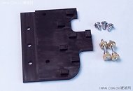
Relatively unknown to the west, yet popular in the Asian OEM and retail markets, Chinese component cooler designer Dongwon has innovated a modular full-coverage design for its water-block which boosts its compatibility. The block serves as a simple answer to NVIDIA's almost ever-changing reference PCB design for its single-GPU GeForce GTX 200 series accelerators. The design allows this water-block to fit the P651 (65 nm GeForce GTX 260 and GTX 280), P654 (first versions of 55 nm GeForce GTX 260 and GTX 285), and the newer P897 PCB design for the 55 nm cards.

The full-coverage block consists of two segments: the main unit which provides coverage for the GPU, the memory and the NVIO2 processor; and the second segment that covers the VRM area. The segment's grooves are designed to cover the LFPAK VRM arrangement on P651 and P654, while it can be detached to allow the rest of the block to be used on the P897. We're not entirely sure if the design concept circled around compatibility with different PCB designs, though it ends up being the block's most useful application. Although the company has seemingly no presence in the western retail channels, one can expect this block to come factory-fitted on graphics cards.

Leadtek Launches New WinFast GTX260 55nm EXTREME+

LEADTEK Research Inc., world acclaimed for its extremevisual graphics leading brand technology, proudly announces its latest WinFast GTX 260 EXTREME+ with a new graphics card packaging design. Based on the Best-in-class NVIDIA GTX 260 chipsets, this thoroughbred graphics card delivers advanced performance with the best cooling silent fansink. Its overclocking capability is sure to bring users a fantasy visual effect. Together with the launch of the graphics card, Leadtek debuts a new packaging design. The latter replaces the former robots with a series of top speed cars as the key visual. This original concept aims to vaunt Leadtek's corporate spirit of "high quality & speedy performance" that gives users an altogether new visual impression.

WinFast GTX 260 EXTREME+ is powered up with 2nd Generation NVIDIA Unified Architecture and enables the rendering of multiple, true-to-life characters in complex and dynamic virtual worlds. In addition, the latest parallel computing architecture with massive independent processing cores enables GTX 260 EXTREME+ to execute the most intricate non-gaming applications via CUDA language. This includes acceleration of the art design application - science simulation application or transcoding of video to a personal video player up to 7X faster than the CPU.

55nm GeForce GTX260 by Inno3D Found on Sale in Japan

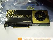
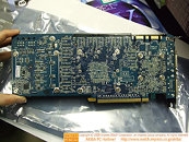
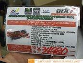
It seems that the first graphics card using NVIDIA's latest 55nm fabrication process has in fact reached retail earlier than the January 2009 release date we had previously anticipated. A Japanese technology website has photos of an Inno3D GeForce GTX260 Gold featuring a factory overclocked, 216 SP chip, made by the 55nm process. What is interesting is that Inno3D have clearly advertised this fact by displaying 55nm on the product and in the product description. The core clock is set at 620Mhz with a memory clock of 1050Mhz, there is no information as yet on the shader clock. It can also be seen that there are no memory chips on the rear of the PCB, this means that all the memory chips are cooled by the stock cooler and there is no longer a need for backplates, as seen on many 65nm GT200 based cards. The pricing however does seem a little steep, with today's exchange rate, this would set you back around $390 USD, with online stores selling the 65nm equivalent for over $100 less, one would hope that the price will drop before it reaches the rest of the world's shores.
Return to Keyword Browsing
Dec 20th, 2024 00:34 EST change timezone

New Forum Posts

Popular Reviews

Controversial News Posts