News Posts matching #Hawaii

Return to Keyword Browsing

Radeon R9 280X is Rebranded HD 7970 GHz Edition

AMD's approach to the next-generation product stack isn't structured too differently from that of NVIDIA's current. The company is launching just one big (high-end) chip, codenamed "Hawaii," based on which it's launching the Radeon R9 290X. It's been detailed to death in our older posts. The Radeon R9 280X, on the other hand, is we're hearing a re-badged Radeon HD 7970 GHz Edition. At the most, expect a slight clock speed bump, and a different reference-design board, but for the most part, it's shaping up to be identical. The approach draws parallels with the NVIDIA's lineup. The Radeon R9 290X is expected to compete with the GeForce GTX TITAN, R9 290 with GTX 780, and R9 280X with the GTX 770. While launch of the R9 290 series will be tightly controlled by AMD (i.e., don't expect non-reference designs for a while), the R9 280X will launch entirely by non-reference designs. The three cards will launch a little later this week.
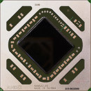
AMD "Hawaii" R9 290X GPU Specifications Revealed

Here are the first set of specifications for AMD's next high-end GPU silicon, on which the company will no doubt carve out several SKUs from. Codenamed "Hawaii," and slated for unveiling on the 26th in, well, Hawaii, the 28 nm chip is what AMD will take NVIDIA's GK110 silicon head-on with. It is based on AMD's second-generation Graphics CoreNext micro-architecture.

With an estimated die-area of 430 mm² (18% bigger than "Tahiti,") the chip physically features 2,816 stream processors (SPs) spread across 44 clusters with 64 SPs each (a 37.5% increase over "Tahiti"). The chip features four independent raster engines, compared to two independent ones on "Tahiti." This could translate into double the geometry processing muscle as "Tahiti," with four independent tessellation units. The memory interface of the chip is expected to be 384-bit wide, based on the GDDR5 specification. Given the way TMUs are arranged on chips based on this architecture, one can deduce 176 TMUs on the chip. The ROP count could be 32 or 48. The chip will feature hardware support for DirectX 11.2, including the much hyped shared resources (mega-texture) feature.

AMD "Hawaii" Press Sample Boxes Surface

Some time in late September, the 25th to be precise, AMD is flying the press at large over to Hawaii, to unveil its "Volcanic Islands" GPU family, with its flagship part, codenamed "Hawaii." This chip is expected to succeed "Tahiti," on which AMD's top-end Radeon HD 7900 series is based. An poster on ChipHell forums leaked these pictures of a press-package of AMD's flagship Hawaii-based graphics card, which has things going both for and against its credibility.

To begin with, the picture shows an audio CD-type jewel case holding Battlefield 4. Given that the game won't launch until late-October, we find it implausible that its release DVDs will be ready a month in advance. There's also a graphic printed on the box that shows the shore of a volcanic island (where magma meets the ocean) in the background, and an AMD logo in the foreground. The thread also contains a few alleged x-ray shots from a different poster, but we're pretty sure that they're of a motherboard. Nice try.

AMD's Answer to GeForce GTX 700 Series: Volcanic Islands

GPU buyers can breathe a huge sigh of relief that AMD isn't fixated with next-generation game consoles, and that its late-2013 launch of its next GPU generation is with good reason. The company is building a new GPU micro-architecture from the ground up. Codenamed "Volcanic Islands," with members codenamed after famous islands along the Pacific Ring of Fire, the new GPU family sees AMD rearranging component-hierarchy within the GPU, in a big way.

Over the past three GPU generations that used VLIW5, VLIW4, and Graphics CoreNext SIMD architectures, the component hierarchy was essentially untouched. According to an early block-diagram of one of the GPUs in the series, codenamed "Hawaii," AMD will designate parallel and serial computing units. Serial cores based on either of the two architectures AMD is licensed to use (x86 and ARM), could handle part of the graphics processing load. The stream processors of today make up the GPU's parallel processing machinery.
Return to Keyword Browsing
Dec 18th, 2024 05:05 EST change timezone

New Forum Posts

Popular Reviews

Controversial News Posts