News Posts matching #IMFlash Technology

Return to Keyword Browsing

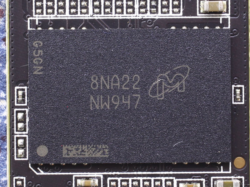
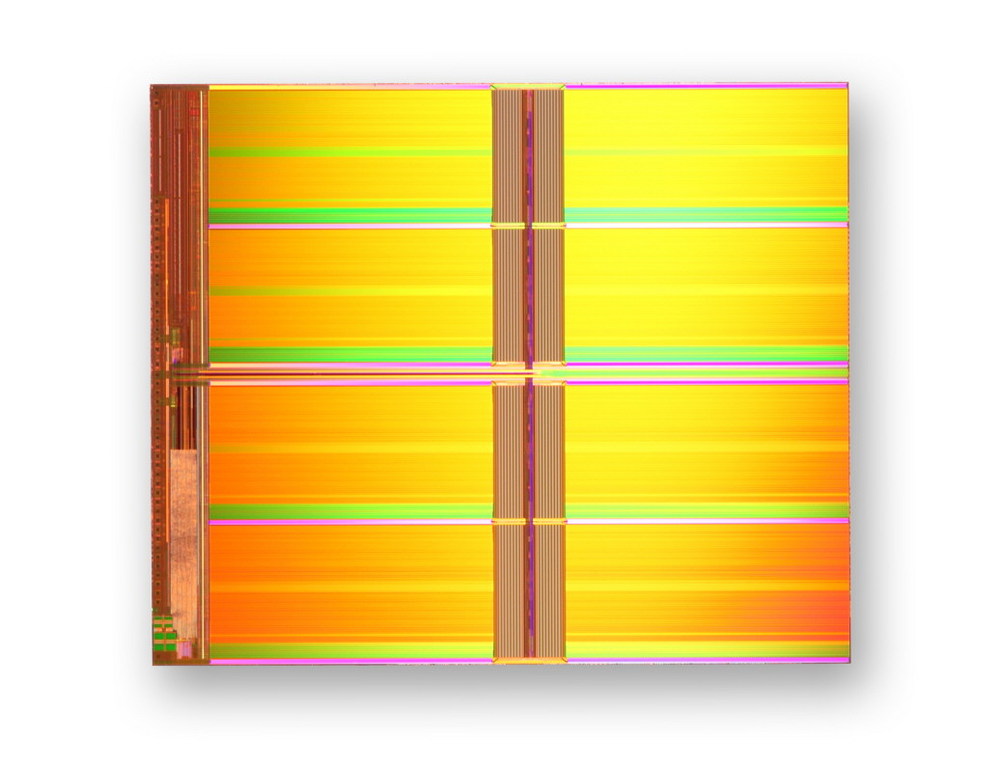
Micron Tapes Out 128-layer 3D NAND Flash Memory

Micron Technology has taped out its 4th generation 3D NAND flash memory with 128 layers. This paves the way for mass production and product implementations in 2020. The 4th gen 3D NAND by Micron continues to use a CMOS-under-array design, but with Replacement Gate (RG) Technology instead of Floating Gate, which Micron and the erstwhile IMFlash Technology had been using for years. Micron is currently mass-producing 96-layer 3D NAND flash, and TLC remains the prominent data-storage physical layer despite the advent of QLC (4 bits per cell).

Micron comments that this 4th gen 128-layer 3D NAND will be a stopgap restricted to a select few applications, and may not see the kind of adoption as its current 96-layer chips. The company appears to be more focused on its evolution, possibly the 5th generation 3D NAND, which are expected to bring tangible cost-per-bit gains for the company, as it transitions to a newer silicon fabrication node, and implements even newer technologies besides RG. "We achieved our first yielding dies using replacement gate or "RG" for short. This milestone further reduces the risk for our RG transition. As a reminder, our first RG node will be 128 layers and will be used for a select set of products. We don't expect RG to deliver meaningful cost reductions until FY2021 when our second-generation RG node is broadly deployed. Consequently, we are expecting minimal cost reductions in NAND in FY2020. Our RG production deployment approach will optimize the ROI of our NAND capital investments," said Sanjay Mehrotra, CEO and president of Micron.

Intel to Move 3D XPoint Memory Manufacturing to China

With its IMFlash Technology joint-venture with Micron coming to an end, Intel is finding itself with manufacturing challenges for its memory businesses. The company holds IP to both 3D NAND flash and its own invention 3D XPoint memory, which it believes will succeed NAND flash in performance and endurance. The company is now mulling to move manufacturing of 3D XPoint to a foundry in China. Intel currently manufactures this exotic new memory at an IMFlash Technology facility in Utah. Intel's $1.3 billion stake-sale to Micron pushes it out of this facility.

Under the terms of the stake-sale, Micron allows Intel to continue to manufacture 3D XPoint at IMFlash for a year, after which it must manufacture it elsewhere. The transfer of stake is scheduled for October 31st, which means Intel's manufacturing in Utah will continue till October 2020. In the meantime, Intel is planning to move manufacturing to its Fab 68, located in Dalian, China. Intel is now manufacturing 1st and 2nd generation 3D Xpoint, while its 3rd generation is under development, and was earlier slated for initial manufacturing at Intel's Fab 11X in New Mexico, USA. It's not known if Intel has changed these plans. 3rd generation 3D XPoint hits mass-production in 2021.

Intel-Micron Divorce Gets Messy, Micron Employee Served Court Order to Return 3D XPoint IP

Intel and Micron Technology have parted ways from the IMFlash Technology joint-venture that set out to win the emerging non-volatile memory market with limited success. The two are now locked in numerous legal skirmishes arising from the disjointing of a major high-technology alliance, as employees migrate to either company. One such former Intel engineering-manager is in the middle of a legal spat, named Doyle Rivers. Rivers jumped ship from Intel to Micron Technology, allegedly carrying with him a large amount of trade-secrets and IP related to Intel's 3D XPoint memory and Optane products.

Intel Tuesday secured a preliminary injunction from the US District Court for the Eastern District of California, Sacramento Division, which tells Rivers to not possess, use, or disclose any confidential Intel information related to the company's 3D XPoint or Optane products, including personnel working on those products; and to return any such possessions to Intel. Rivers' defense claims Intel gets nothing from this injunction. In a telephonic interview with The Register, Daniel Sakaguchi, a partner at Alto Litigation in San Francisco, representing Rivers, stated "Mr. Rivers doesn't have anything to return," adding "We continue to take the position that Intel's claims are greatly exaggerated."

NAND Flash Prices May See Further Drops in 2019, DRAM to Remain Flat

Solid-state drives are cheaper than ever, thanks to systematic decline in NAND flash prices owing both to oversupply and increases in densities. NAND flash prices have already declined by 50 percent over 2018, according to a DigiTimes report, and will continue to slide through 2019. ADATA chairman Simon Chen commented that NAND flash makers haven't slowed down capacity expansions, and 2019 could witness an even bigger drop in prices than 2018.

Major NAND flash makers such as IMFlash Technology, SK Hynix, Samsung, Western Digital, Toshiba, have already taped out their 96-layer 3D NAND flash products, which could enter volume production in the first half of 2019. This could impact prices of existing swelling inventories of products based on 64-layer NAND flash. In theory, the 96-layer chips introduce 50 percent increases in densities. Adoption of newer technologies such as QLC (4 bits per cell) will expand densities even further. The same report also projects that DRAM prices could largely remain flat throughout 2019. Most NAND flash makers also happen to make DRAM, and could balance their NAND flash losses with DRAM profits.

Intel Intros 660p Series M.2 NVMe SSDs with QLC NAND Flash

Intel Tuesday introduced the new SSD 660p series M.2 NVMe solid state drives. At the heart of these drives is the new 64-layer 3D QLC (quadruple level cell, or 4 bits per cell) NAND flash memory by IMFlash Technology (an Intel and Micron joint-venture). This memory is mated with a SIlicon Motion SMI 2263 controller. This chip is a derivative of the popular SMI2262EN, built on a newer process, with support for QLC NAND flash, compacted to have a smaller PCB footprint, and is driven by a custom firmware by Intel. The drives use over 10% of the QLC NAND flash area as SLC cache. The 660p series comes in three variants based on size - 512 GB, 1 TB, and 2 TB. The prices are the biggest dividend of QLC: the 512 GB variant goes for USD $99.99, the 1 TB variant at $199.99, and the 2 TB variant for $399.99.

Built in the M.2-2280 form-factor, the SSD 660p series drives feature PCI-Express 3.0 x4 interface. Intel's pricing puts these drives close to competing drives with PCIe x2 interface, but offering higher transfer rates thanks to the wider bus. It's also interesting to note here that the controller is cushioned by a DRAM cache (something PCIe x2 drives tend to lack, to keep costs down). Performance numbers differ by variant, and the 512 GB drive is the slowest, sequentially reading at speeds of up to 1500 MB/s, with up to 1000 MB/s sequential writes; up to 90,000 4K random reads, and up to 220,000 IOPS 4K random writes. The 1 TB and 2 TB variants both sequentially read and write at up to 1800 MB/s. The 1 TB variant offers 150,000 IOPS 4K random reads, and up to 220,000 IOPS random writes; while the 2 TB variant has 4K random reads/writes numbers of 220,000 IOPS.

China's Tsinghua Unigroup to Manufacture 3D NAND Flash for Intel

In a bid to ensure sufficient supply of NAND flash memory to meet the growing demands of not just PC, but also smartphone markets, China's Tsinghua Unigroup and Intel are in talks to license-manufacture 64-layer 3D NAND flash, based on existing IMFlash Technologies designs. IMFlash is a joint-venture between Intel and Micron Technology. Tsinghua Unigroup is one of the biggest beneficiaries of the Chinese Government's ambitious plan to invest RMB 1 trillion (USD $158 billion) over the next five years, to increase China's semiconductor self-sufficiency to 70 percent, by 2025.

The move will significantly increase supply of NAND flash memory, and is seen as a market threat to Korean NAND flash giants Samsung and SK Hynix, and Japanese Toshiba. IMFlash Technology released its first 64-layer 3D NAND flash to the market in 2017, and is currently developing a 96-layer 3D NAND flash chip, which, along with newer 10 nm-class silicon fabrication process, could double densities over the current 64-layer chips.

Intel Intros SSD 545s Mainstream SATA SSD

Intel today announced the SSD 545s line of mainstream SATA solid-state drives. Built in the 7 mm-thick 2.5-inch form-factor with SATA 6 Gbps interface, the drives combine new 64-layer 3D TLC NAND flash memory by IMFlash Technology, with a Silicon Motion SMI SM2259 controller, and a custom firmware by Intel. For now, the drive is only available in one capacity, 512 GB. It offers sequential transfer speeds of up to 550 MB/s, with up to 500 MB/s sequential writes; 4K random read performance of up to 75,000 IOPS, 4K random write performance of up to 85,000 IOPS, and endurance of at least 144 TBW. Besides common SSD features such as NCQ and TRIM, the drive offers native 256-bit AES encryption. Available now, and backed by a 3-year warranty, the SSD 545s 512 GB is priced at USD $179.99.

Intel Readies TLC 3D NAND Flash Based 610P Series PCIe SSD for 2017

Intel is readying a follow-on to its 600P series performance-segment PCIe solid-state drive (SSD) series, with the 610P series. Built in the M.2-2280 form-factor, with PCIe gen 3.0 x4 bus interface, and support for the NVMe protocol, the SSD 610P will be based on TLC 3D NAND flash by IMFlash Technology, the company's joint-venture with Micron Technology. The SSD 610P series will come in capacities of 128 GB, 256 GB, 512 GB, 1 TB, and 2 TB.

The company is also working on a smaller M.2-1620 variant for notebooks and SFF desktops, which will feature a BGA version of the SSD. These are multi-chip modules of NAND flash stacks and SSD controllers bundled into single packages. The BGA variants will come in sizes of 128 GB, 256 GB, and 512 GB. Not much else (performance figures) are known about these drives, except that Intel plans to release these towards Q4 2017 (after September).

Intel Unveils DC S3510 SSDs for the Data Center

Intel quietly announced availability of its DC S3510 SSDs for data centers. Built in the 2.5-inch form-factor, with SATA 6 Gb/s interface, these drives feature SET (standard-endurance technology) MLC NAND flash built by IMFlash Technology, on a 16 nanometer node, which can take in up to 880 TBW. Its controller offers native 256-bit AES encryption. The drive is available in capacities of 80 GB, 120 GB, 240 GB, 480 GB, 800 GB, 1.2 TB, and 1.6 TB. The table below shows sequential and 4K random access performance figures by the company for each model. The drives are backed by 5-year warranties, and are available in the OEM channel. Its target consumers are low-cost dedicated hosting providers.

Intel and Micron develop first-ever 128 Gb NAND Flash memory chip

Flash buddies Intel and Micron have today announced a significant breakthrough in terms of NAND density, the first 128 Gb (16 GB) MLC NAND memory chip. Manufactured on 20 nm process technology, this 128 Gb chip complies with the ONFI 3.0 specification (enabling speeds of up to 333 megatransfers per second) and can be used for new, high-capacity solid state drives, as well as for next-generation tablets, smartphones and other portable devices.

According to Intel and Micron, this milestone was made possible by the use of a new, innovative cell structure that 'breaks the scaling constraints of the standard NAND floating gate cell by integrating the first Hi-K/metal gate stack on NAND production.'

Intel, Micron Extend NAND Flash Technology Leadership, Introduce 20 nm NAND Flash

Intel Corporation and Micron Technology Inc. today introduced a new, finer 20-nanometer (nm) process technology for manufacturing NAND flash memory. The new 20nm process produces an 8-gigabyte (GB) multi-level cell (MLC) NAND flash device, providing a high-capacity, small form factor storage option for saving music, video, books and other data on smartphones, tablets and computing solutions such as solid-state drives (SSDs).

The growth in data storage combined with feature enhancements for tablets and smartphones is creating new demands for NAND flash technology, especially greater capacity in smaller designs. The new 20nm 8GB device measures just 118mm² and enables a 30 to 40 percent reduction in board space (depending on package type) compared to the companies' existing 25nm 8GB NAND device. A reduction in the flash storage layout provides greater system level efficiency as it enables tablet and smartphone manufacturers to use the extra space for end-product improvements such as a bigger battery, larger screen or adding another chip to handle new features.
Return to Keyword Browsing
May 11th, 2024 02:29 EDT change timezone

New Forum Posts

Popular Reviews

Controversial News Posts