News Posts matching #Intel

Return to Keyword Browsing

ASML High-NA EUV Twinscan EXE Machines Cost $380 Million, 10-20 Units Already Booked

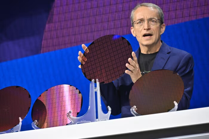
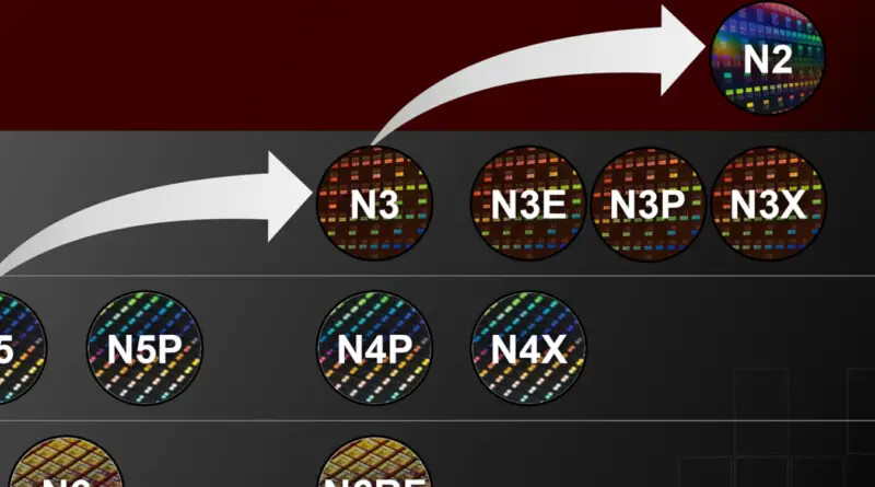
ASML has revealed that its cutting-edge High-NA extreme ultraviolet (EUV) chipmaking tools, called High-NA Twinscan EXE, will cost around $380 million each—over twice as much as its existing Low-NA EUV lithography systems that cost about $183 million. The company has taken 10-20 initial orders from the likes of Intel and SK Hynix and plans to manufacture 20 High-NA systems annually by 2028 to meet demand. The High-NA EUV technology represents a major breakthrough, enabling an improved 8 nm imprint resolution compared to 13 nm with current Low-NA EUV tools. This allows chipmakers to produce transistors that are nearly 1.7 times smaller, translating to a threefold increase in transistor density on chips. Attaining this level of precision is critical for manufacturing sub-3 nm chips, an industry goal for 2025-2026. It also eliminates the need for complex double patterning techniques required presently.

However, superior performance comes at a cost - literally and figuratively. The hefty $380 million price tag for each High-NA system introduces financial challenges for chipmakers. Additionally, the larger High-NA tools require completely reconfiguring chip fabrication facilities. Their halved imaging field also necessitates rethinking chip designs. As a result, adoption timelines differ across companies - Intel intends to deploy High-NA EUV at an advanced 1.8 nm (18A) node, while TSMC is taking a more conservative approach, potentially implementing it only in 2030 and not rushing the use of these lithography machines, as the company's nodes are already developing well and on time. Interestingly, the installation process of ASML's High-NA Twinscan EXE 150,000-kilogram system required 250 crates, 250 engineers, and six months to complete. So, production is as equally complex as the installation and operation of this delicate machinery.

AMD Develops ROCm-based Solution to Run Unmodified NVIDIA's CUDA Binaries on AMD Graphics

AMD has quietly funded an effort over the past two years to enable binary compatibility for NVIDIA CUDA applications on their ROCm stack. This allows CUDA software to run on AMD Radeon GPUs without adapting the source code. The project responsible is ZLUDA, which was initially developed to provide CUDA support on Intel graphics. The developer behind ZLUDA, Andrzej Janik, was contracted by AMD in 2022 to adapt his project for use on Radeon GPUs with HIP/ROCm. He spent two years bringing functional CUDA support to AMD's platform, allowing many real-world CUDA workloads to run without modification. AMD decided not to productize this effort for unknown reasons but did open-source it once funding ended per their agreement. Over at Phoronix, there were several benchmarks testing AMD's ZLUDA implementation over a wide variety of benchmarks.

Benchmarks found that proprietary CUDA renderers and software worked on Radeon GPUs out-of-the-box with the drop-in ZLUDA library replacements. CUDA-optimized Blender 4.0 rendering now runs faster on AMD Radeon GPUs than the native ROCm/HIP port, reducing render times by around 10-20%, depending on the scene. The implementation is surprisingly robust, considering it was a single-developer project. However, there are some limitations—OptiX and PTX assembly codes still need to be fully supported. Overall, though, testing showed very promising results. Over the generic OpenCL runtimes in Geekbench, CUDA-optimized binaries produce up to 75% better results. With the ZLUDA libraries handling API translation, unmodified CUDA binaries can now run directly on top of ROCm and Radeon GPUs. Strangely, the ZLUDA port targets AMD ROCm 5.7, not the newest 6.x versions. Only time will tell if AMD continues investing in this approach to simplify porting of CUDA software. However, the open-sourced project now enables anyone to contribute and help improve compatibility. For a complete review, check out Phoronix tests.

NVIDIA to Create AI Semi-custom Chip Business Unit

NVIDIA is reportedly working to set up a new business unit focused on designing semi-custom chips for some of its largest data-center customers, Reuters reports. NVIDIA dominates the AI HPC processor market, although even its biggest customers are having to shop from its general lineup of A100 series and H100 series HPC processors. There are reports of some of these customers venturing out of the NVIDIA fold, wanting to develop their own AI processor designs. It is to cater to exactly this segment that NVIDIA is setting up the new unit.

A semi-custom chip isn't just a bespoke chip designed to a customer's specifications. It is co-developed by NVIDIA and its customer, using mainly NVIDIA IP blocks, but also integrating some third-party IP blocks the customer may want; and more importantly, approach semiconductor fabrication companies such as TSMC, Samsung, or Intel Foundry Services as separate entities from NVIDIA for their wafer allocation. For example, a company like Google may have a certain amount of wafer pre-allocation with TSMC (eg: for its Tensor SoCs powering the Pixel smartphones), which it may want to tap into for a semi-custom AI HPC processor for its cloud business. NVIDIA assesses a $30 billion TAM for this specific business unit—that's all its current customers wanting to pursue their own AI processor projects, who will now be motivated to stick to NVIDIA.

IDC Forecasts Artificial Intelligence PCs to Account for Nearly 60% of All PC Shipments by 2027

A new forecast from International Data Corporation (IDC) shows shipments of artificial intelligence (AI) PCs - personal computers with specific system-on-a-chip (SoC) capabilities designed to run generative AI tasks locally - growing from nearly 50 million units in 2024 to more than 167 million in 2027. By the end of the forecast, IDC expects AI PCs will represent nearly 60% of all PC shipments worldwide.

"As we enter a new year, the hype around generative AI has reached a fever pitch, and the PC industry is running fast to capitalize on the expected benefits of bringing AI capabilities down from the cloud to the client," said Tom Mainelli, group vice president, Devices and Consumer Research. "Promises around enhanced user productivity via faster performance, plus lower inferencing costs, and the benefit of on-device privacy and security, have driven strong IT decision-maker interest in AI PCs. In 2024, we'll see AI PC shipments begin to ramp, and over the next few years, we expect the technology to move from niche to a majority."

Intel Begins APX and AVX10 Enablement in Linux, Setting Foundation for Granite Rapids

Intel has begun rolling out software binaries compiled with support for upcoming Advanced Performance Extensions (APX) and Advanced Vector Extensions 10 (AVX10) instruction set extensions in their Clear Linux distribution, ahead of any processors officially supporting these capabilities launching. Clear Linux is focusing first on optimized APX and AVX10 versions of foundational software libraries like glibc and Python. This builds on Clear Linux's existing support for optimized x86-64-v2, v3, and v4 code paths, leveraging the latest microarchitectural features of each Intel CPU generation. The rationale is to prepare Clear Linux to fully leverage the performance potential of next-generation Intel Xeon server processors, code-named Granite Rapids, expected to launch later this year.

Granite Rapids will introduce AVX10.1/512 instructions as well as the new APX capabilities, which are currently not well documented implementation wise. By rolling out APX/AVX10 support in software now, Clear Linux aims to have an optimized ecosystem ready when the new processors officially ship. Initially, APX and AVX10 support is being added using the existing GCC compiler. Still, Clear Linux notes they will transition to using the upcoming GCC 14 release with more mature support for these instruction sets. The goal is to eventually have many Clear Linux packages compiled with APX/AVX10 code paths to maximize performance on future Intel CPUs. This continues Clear Linux's strategy of leveraging Intel's latest hardware capabilities in software.

German Court Prohibits Intel Processor Sales Amid Patent Dispute

According to Financial Times, a regional court in Düsseldorf, Germany, created a significant setback for Intel on Wednesday, issuing an injunction prohibiting sales of some of its processors due to allegations they infringe on a patent held by R2 Semiconductor. R2, a technology firm based in Palo Alto, California, accused Intel of violating its patent related to processor voltage regulation. The ruling applies to Intel's 10th, 11th, and 12th generation Core processors, known as Ice Lake, Tiger Lake, and Alder Lake, as well as its Ice Lake Xeon server SKUs. Newer processors generations (13th, 14th, etc.) don't infringe the patent. Even though Intel noted that it plans to appeal the decision, the ramifications could extend beyond the company itself. Industry experts warn the court order could lead to a sweeping ban on products containing the disputed Intel chips, including laptops and pre-built PCs from major manufacturers like HP and Dell. R2 has waged an ongoing legal fight across multiple jurisdictions to defend its intellectual property.

After initially filing suit against Intel in the United States, R2 shifted its efforts to Germany and other European countries after its patent was invalidated stateside. Intel strongly denied R2's patent infringement claims, alleging the company's entire business model relies on extracting legal settlements through serial litigation. Intel believes the injunction serves only R2's financial interests while harming consumers, businesses, and the economy. The two firms traded barbs in official statements about the case. R2's CEO, David Fisher, rebuffed Intel's characterization of his company, saying it has only targeted Intel for infringement of its clear IP rights. As the war of words continues, the practical impact of the German court's decision remains uncertain, pending Intel's appeal. However, the preliminary injunction demonstrates the massive financial consequences at stake in battles over technological patents.

Windows 11 DirectML Preview Supports Intel Core Ultra NPUs

Chad Pralle, Principle Technical Program Manager at Microsoft's Windows AI NPU division has introduced the DirectML 1.13.1 and ONNX Runtime 1.17 APIs—this appears to be a collaborative effort—Samsung was roped in to some degree, according to Microsoft's announcement and a recent Team Blue blog entry. Pralle and his team are suitably proud of this joint effort that involved open source models: "we are excited to announce developer preview support for NPU acceleration in DirectML, the machine learning platform API for Windows. This developer preview enables support for a subset of models on new Windows 11 devices with Intel Core Ultra processors with Intel AI boost."

Further on in Microsoft's introductory piece, Samsung Electronics is announced as a key launch partner—Hwang-Yoon Shim, VP and Head of New Computing H/W R&D Group stated that: "NPUs are emerging as a critical resource for broadly delivering efficient machine learning experiences to users, and Windows DirectML is one of the most efficient ways for Samsung's developers to make those experiences for Windows." Microsoft notes that NPU support in DirectML is still "a work in progress," but Pralle and his colleagues are eager to receive user feedback from the testing community. It is currently "only compatible with a subset of machine learning models, some models may not run at all or may have high latency or low accuracy." They hope to implement improvements in the near future. The release is limited to modern Team Blue hardware, so NPU-onboard AMD devices are excluded at this point in time, naturally.

Samsung Lands Significant 2 nm AI Chip Order from Unnamed Hyperscaler

This week in its earnings call, Samsung announced that its foundry business has received a significant order for a two nanometer AI chips, marking a major win for its advanced fabrication technology. The unnamed customer has contracted Samsung to produce AI accelerators using its upcoming 2 nm process node, which promises significant gains in performance and efficiency over today's leading-edge chips. Along with the AI chips, the deal includes supporting HBM and advanced packaging - indicating a large-scale and complex project. Industry sources speculate the order may be from a major hyperscaler like Google, Microsoft, or Alibaba, who are aggressively expanding their AI capabilities. Competition for AI chip contracts has heated up as the field becomes crucial for data centers, autonomous vehicles, and other emerging applications. Samsung said demand recovery in 2023 across smartphones, PCs and enterprise hardware will fuel growth for its broader foundry business. It's forging ahead with 3 nm production while eyeing 2 nm for launch around 2025.

Compared to its 3 nm process, 2 nm aims to increase power efficiency by 25% and boost performance by 12% while reducing chip area by 5%. The new order provides validation for Samsung's billion-dollar investments in next-generation manufacturing. It also bolsters Samsung's position against Taiwan-based TSMC, which holds a large portion of the foundry market share. TSMC landed Apple as its first 2 nm customer, while Intel announced 5G infrastructure chip orders from Ericsson and Faraday Technology using its "Intel 18A" node. With rivals securing major customers, Samsung is aggressively pricing 2 nm to attract clients. Reports indicate Qualcomm may shift some flagship mobile chips to Samsung's foundry at the 2 nm node, so if the yields are good, the node has a great potential to attract customers.

Intel NEX "Bartlett Lake-S" CPUs Reportedly in Pipeline

Supply chain insiders have claimed that Intel is working on extending the lifespan of its LGA 1700 platform—a BenchLife report proposes that the "Bartlett Lake-S" processor family is due soon, courtesy of Team Blue's Network and Edge (NEX) business group. Only a few days ago, the rumor mill had placed "Bartlett Lake-S" CPUs in a mainstream desktop category, due to alleged connections with the Raptor Lake-S Refresh series—the former is also (supposedly) based on the Intel 7 processor process. BenchLife believes that DDR4 and DDR5 memory will be supported, but with no mention of possible ECC functionality. Confusingly, chip industry tipsters believe that the unannounced processors could be launched as 15th Gen Core parts.

BenchLife has a history of discovering and reporting on Intel product roadmaps—apparently Bartlett Lake-S can leverage the same core configurations as seen on Raptor Lake-S; namely 8 Raptor Cove P-Cores and 16 Gracemont E-Cores. An insider source claims that a new pure P-Core-only design could exist, sporting up to twelve Raptor Cove units. According to a leaked Bartlett Lake-S series specification sheet: "the iGPU part will use (existing) Intel Xe architecture, up to Intel UHD Graphics 770." The publication alludes to some type of AI performance enhancement as a distinguishing feature for Bartlett Lake-S, when lined up against 14th Gen Core desktop SKUs. Folks salivating at the prospect of a mainstream DIY launch will have to wait and see (according to BenchLife's supply chain insider): "judging from various specifications, this product belonging to the Intel NEX business group may also be decentralized to the consumer market, but the source did not make this part too clear and reserved some room for maneuver."

ASRock Releases New BIOS for More Performance on Intel 600/700 Series Motherboards

ASRock releases new BIOS for Intel 600/700 series motherboards, the updated BIOS is able to drastically improve CPU performance on 14th gen non-K series processors up to 10% with I7-14700 by Cinebench R23. The performance gain is benefit from Intel's latest microcode and ASRock is the first to implement this new update before Chinese New Year, the new BIOS for Z790 series motherboards are as below, 600 & B760 series will be updated shortly!

You can find the full list of motherboards and BIOS versions in the table below.

Intel Looking to Grab Microsoft Xbox Semi-custom SoC Business from AMD

Intel is reportedly pitching Microsoft to work on an "all American" semi-custom SoC for Microsoft's next Xbox generation that succeeds the Series X/S. The company's main pitch to Microsoft is the fact that the chip would be made entirely in the US, including its silicon fabrication and packaging. Microsoft currently relies on AMD for its SoC, which combines an AMD "Zen 2" CPU with a powerful RDNA2 iGPU that meets DirectX 12 Ultimate requirements.

Intel's semi-custom chip could be functionally the same, albeit based on its next generation CPU and graphics microarchitectures. Strengthening Intel's case is the fact that it now has a contemporary high performance gaming graphics architecture in Xe "Alchemist," and is on course to launch its successor, the Xe² "Battlemage," later this year. The company also made huge strides with chiplet-based SoCs as demonstrated with "Meteor Lake." Intel's semi-custom SoC for Microsoft could combine any of its upcoming CPU microarchitectures, such as "Lunar Lake," or "Panther Lake," and an iGPU based on "Battlemage" or Xe³ "Celestial." This chip could also integrate a next generation NPU if the platform calls for one. This wouldn't be Intel's first rodeo with powering a console; in fact the very first Microsoft Xbox was powered by a Pentium 3 "Coppermine" CPU, paired with a discrete GeForce 3 GPU supplied by NVIDIA.

TSMC Overtakes Intel and Samsung to Become World's Largest Semiconductor Maker by Revenue

Taiwan Semiconductor Manufacturing Company (TSMC) has reached a significant milestone, overtaking Intel and Samsung to become the world's largest semiconductor maker by revenue. According to Taiwanese financial analyst Dan Nystedt, TSMC earned $69.3 billion in revenue in 2023, surpassing Intel's $63 billion and Samsung's $58 billion. This is a remarkable achievement for the Taiwanese chipmaker, which has historically lagged behind Intel and Samsung in terms of revenue despite being the world's largest semiconductor foundry. TSMC's meteoric rise has been fueled by the increased demand for everything digital - from PCs to game consoles - during the coronavirus pandemic in 2020, and AI demand in the previous year. With its cutting-edge production capabilities allowing it to manufacture chips using the latest process technologies, TSMC has pulled far ahead of Intel and Samsung and can now charge a premium for its services.

This is reflected in its financials. For the 6th straight quarter, TSMC's Q4 2023 revenue of $19.55 billion also beat Intel's $15.41 billion and Samsung's $16.42 billion chip division revenue. As the world continues its rapid transformation in the AI era of devices, TSMC looks set to hold on to its top position for the foreseeable future. Its revenue and profits will likely continue to eclipse those of historical giants like Intel and Samsung. However, a big contender is Intel Foundry Services, which is slowly starting to gain external customers. If IFS takes off and new customers start adopting Intel as their foundry of choice, team blue could regain leadership in the coming years.

Intel Readies Xeon W3500 and W2500 "Sapphire Rapids Refresh" Series HEDT Processors

It turns out that the 60-core Xeon W9-3595X leak from last week is part of a 14-SKU mid-lifecycle refresh of the Xeon W LGA4677 series targeting the workstation and HEDT markets. The underlying microarchitecture and silicon at the heart of these is "Sapphire Rapids Refresh," it's essentially the same as "Sapphire Rapids," but with CPU core-count increases across the SKUs. If you recall, the "Sapphire Rapids" MCM has a maximum core-count of 60-core/120-thread which is maxed out in Xeon Scalable server processors, but only hit up to 56-core/112-thread with the original W3400 and W2400 series HEDT/workstation chips. This unused 4-core headroom, combined with increases in clock speeds, is how Intel plans to create these 14 SKUs across the new W3500 and W2500 product lines.

As with the original W3400 and W2400 series; what set the W3500 series chips apart from the W2500 series, is the I/O. The W3500 series gets 8-channel DDR5 memory and 128 PCIe Gen 5 lanes, while the W2500 series chips get 4-channel DDR5 memory and 64 PCIe Gen 5 lanes. As we mentioned, this refresh is all about increasing the CPU core counts at existing price points. The top W9-3595X is a 60-core/120-thread chip, compared to the 56-core/112-thread W9-3495X it's replacing. The new W9-3575X gets a massive 8-core uplift, and is now a 44-core/88-thread processor, compared to the 36-core/72-thread W9-3475X. The W7-3565X is 32-core/64-thread, compared to the 28-core/56-thread W7-3465X.

Intel, Microsoft, and Cirrus Logic Collaborate on Lunar Lake Reference Laptop Design

Intel, Microsoft, and a fabless semiconductor company making analog, mixed-signal, and audio DSP, Cirrus Logic, have collaborated on a new reference laptop design to showcase the upcoming Lunar Lake mobile CPUs. The goal is to enable "cool, quiet, and high-performance" laptops that push the boundaries of efficiency, thickness, and acoustics. The reference design incorporates three key components from Cirrus Logic - the CP9314 power converter chip, CS42L43 audio codec, and CS35L56 amplifier. The CP9314 is the most critical element, using advanced power conversion technology to improve Lunar Lake's power efficiency significantly. This enables thinner and quieter laptops with longer battery life. The codec and amplifier chips also play a role, providing high-quality audio with next-generation features like spatial audio support.

Together, these Cirrus Logic components aim to highlight Lunar Lake's capabilities for efficiency, performance, and immersive experiences in a thin and light form factor. While details remain scarce on the Lunar Lake CPUs themselves, they are expected to arrive later this year, likely in the second half. If the reference laptops live up to their promises, Lunar Lake could help Intel regain leadership in mobile computing efficiency, which has been lacking since the introduction of Apple's M series SoCs, which have superior battery life. With expert collaboration from Microsoft and Cirrus Logic on the peripheral hardware and software, Lunar Lake may usher in a new generation of cool, quiet, and powerful laptops.

Intel Open Image Denoise v2.2 Adds Metal Support & AArch64 Improvements

An Open Image Denoise 2.2 release candidate was released earlier today—as discovered by Phoronix's founder and principal writer; Michael Larabel. Intel's dedicated website has not been updated with any new documentation or changelogs (at the time of writing), but a GitHub release page shows all of the crucial information. Team Blue's open-source oneAPI has been kept up-to-date with the latest technologies—not only limited to Intel's stable of Xe-LP, Xe-HPG and Xe-HPC components—the Phonorix article highlights updated support on competing platforms. The v2.2 preview adds support for Meteor Lake's integrated Arc graphics solution, and additional "denoising quality enhancements and other improvements."

Non-Intel platform improvements include updates for Apple's M-series chipsets, AArch64 processors, and NVIDIA CUDA. OIDn 2.2-rc: "adds Metal device support for Apple Silicon GPUs on recent versions of macOS. OIDn has already been supporting ARM64/AArch64 for Apple Silicon CPUs while now Open Image Denoise has extended that AArch64 support to work on Windows and Linux too. There is better performance in general for Open Image Denoise on CPUs with this forthcoming release." The changelog also highlights a general improvement performance across processors, and a fix that resolves a crash incident: "when releasing a buffer after releasing the device."

Intel Arrow Lake-S 24 Thread CPU Leaked - Lacks Hyper-Threading & AVX-512 Support

An interesting Intel document leaked out last month—it contained detailed pre-release information that covered their upcoming 15th Gen Core Arrow Lake-S desktop CPU platform, including a possible best scenario 8+16+1 core configuration. Thorough analysis of the spec sheet revealed a revelation—the next generation Core processor family could "lack Hyper-Threading (HT) support." The rumor mill had produced similar claims in the past, but the internal technical memo confirmed that Arrow Lake's "expected eight performance cores without any threads enabled via SMT." These specifications could be subject to change, but tipster—InstLatX64—has uprooted an Arrow Lake-S engineering sample: "I spotted (CPUID C0660, 24 threads, 3 GHz, without AVX 512) among the Intel test machines."

The leaker had uncovered several pre-launch Meteor Lake SKUs last year—with 14th Gen laptop processors hitting the market recently, InstLatX64 has turned his attention to seeking out next generation parts. Yesterday's Arrow Lake-S find has chins wagging about the 24 thread count aspect (sporting two more than the fanciest Meteor Lake Core Ultra 9 processor)—this could be an actual 24 core total configuration—considering the evident lack of hyper-threading, as seen on the leaked engineering sample. Tom's Hardware reckons that the AVX-512 instruction set could be disabled via firmware or motherboard UEFI—if InstLatX64's claim of "without AVX-512" support does ring true, PC users (demanding such workloads) are best advised to turn to Ryzen 7040 and 8040 series processors, or (less likely) Team Blue's own 5th Gen Xeon "Emerald Rapids" server CPUs.

Intel Arc A370M Laptop GPU Transforms into ITX-Sized Desktop GPU

Taiwanese tech maker Advantech has converted Intel's Arc A370M mobile GPU into a desktop graphics card named the EAI-3100. The new card utilizes the same Arc A370M mobile GPU based on the Xe-LP architecture chip as found in laptops but adds more robust cooling to enable desktop-level performance. Specifically, the EAI-3100 implements a large aluminium heatsink spanning the entire PCB, paired with a 40 mm fan active cooling fan. This allows the card to operate at up to 60 Watt TGP (total graphics power), a noticeable increase over the A370M's 35-50 Watt mobile power range. Despite the improved cooling, Advantech has not factory overclocked the EAI-3100, leaving its graphics clock speed unchanged at 1,550 MHz. The card also retains the same PCIe 4.0 x8 interface as the mobile A370M. An 8-pin PCIe power connector has been added, giving headroom for user overclocking attempts.

In terms of gaming performance, the A370M and, by extension, the EAI-3100 deliver playable frame rates at 1080p resolution with medium image quality settings. The card is comparable to NVIDIA's mobile RTX 3050 GPU. As Intel continues optimizing Arc drivers, more gains are expected. The EAI-3100's dual-slot, 6.61-inch design allows compatibility with most desktop PC cases. Between its small size and the A370M's solid 1080p capabilities, this transformed card represents an interesting budget option for gamers seeking a discounted route to Arc's architecture. Despite the diminutive size, this custom cooling solution keeps the A370M at appropriate temperatures for sustained operation, possibly delivering more than the laptop form factor SKU. For video output, the card features two HDMI 2.0b and two DP 1.4a ports.

MAINGEAR Releases Preconfigured MG-1 Gaming PCs, New Ruby and Boosted System Configurations

MAINGEAR, the leader in premium-quality, high-performance gaming PCs, announces its 2024 preconfigured MG-1 gaming PCs, featuring the latest NVIDIA GeForce RTX 40-Series SUPER GPUs. Designed to redefine the gaming experience, these newly announced pre-configured systems, starting at $1,199, offer enhanced performance, diverse options, more memory, larger SSD capacities, and can be had with Windows 11 Pro.

"Refreshing the MG-1 Series to feature the latest gaming hardware and components represents our ongoing commitment to delivering cutting-edge gaming experiences. With the latest Intel & AMD processors, NVIDIA GPUs, including the new SUPERs, and a broader range of options in the MG-1, MAINGEAR continues to set the standard for gaming excellence." - Wallace Santos, CEO of MAINGEAR.

DFI Unveils Embedded System Module Equipped with Intel's Latest AI Processor

DFI, the world's leading brand in embedded motherboards and industrial computers, is targeting the AI application market by launching the embedded system module (SOM) MTH968 equipped with the latest Intel Core Ultra processor. It is the first product integrated with an NPU (Neural Processor Unit) processor, representing the official integration of AI with industrial PCs (IPCs). With the expansion into AI IPC, DFI expects to inject new momentum into the AI edge computing market.

According to the STL Partners report, the potential market value of global edge computing will increase from US$9 billion in 2020 to US$462 billion in 2030, representing a compound annual growth rate (CAGR) of 49%. Therefore, the development of products that utilize the core capabilities of chips to rapidly execute AI edge computing in devices has become a key focus for many major technology companies.

ESL FACEIT Group, Intel, and Acer Expand Strategic Partnership Across Premier Counter-Strike and Dota 2 Competitions

ESL FACEIT Group (EFG), the leading esports and video game entertainment company, and Intel, have today announced the extension and expansion of their partnership with Acer. As the exclusive Original Equipment Manufacturer (OEM) partner, Acer's gaming brand Predator will empower EFG Counter-Strike 2 and Dota 2 competitions across 2024. Intel and EFG have been partners in the esports space for over 20 years, fostering and supporting a passionate global community through world-leading esports events, activations and opportunities. Their vision is shared by Acer, and the mutual desire for progress, innovation, and delivering exceptional experiences has been the catalyst in the success, and now renewal, of their partnership.

"Acer's partnership with Intel and EFG is driven by our shared commitment of supporting the esports community, bringing gameplay to new heights," said Vincent Lin, Associate Vice President, Global Product Marketing and Planning, Acer Inc. "Our latest Predator gaming laptops powered by Intel Core 14th Gen processors provide powerful performance and combine AI-powered features that enhance the overall gaming experience."

Intel Xeon W9-3595X Spotted with 60 Cores, 112 MB of L3 Cache, and 4.60 GHz Frequency

Intel's upcoming high-end desktop (HEDT) processor lineup for enthusiasts and prosumers is around the corner, and today, we managed to see the flagship SKU - the Xeon W9-3595X. Spotted recently on Geekbench benchmarks, this new chip packs a whopping 60 cores and 120 threads, making it Intel's highest core count HEDT offering yet. The Xeon W9-3595X is based on Intel's advanced Sapphire Rapids architecture, built using the Intel 7 process node. It succeeds the previous flagship 56-core W9-3495X, with four additional cores crammed into the new 350 Watt TDP envelope. Clock speeds have taken a slight hit to accommodate the extra cores, with the maximum turbo frequency lowered from 4.8 GHz on the 3495X to 4.6 GHz on the new 3595X.

However, with more cores, the 3595X should still offer a significant multi-threaded performance uplift for heavily parallel workloads. The Xeon W9-3595X will drop into existing LGA-4677 motherboards, like the ASUS PRO WS 790-ACE, after a BIOS update. It features 112 MB of L3 cache, 120 MB of L2 cache (2 MB per core), and continues Intel's push towards higher core counts for enthusiasts, content creators, and workstation users who need maximum multi-threaded horsepower. Pricing and availability details remain unannounced as of now. But with an appearance on public databases, an official launch of the 60-core HEDT juggernaut seems imminent. These new Sapphire Rapids SKUs will likely have extra AI features, like dedicated AI acceleration engines, in the same manner that server-class SKUs do.

NVIDIA Faces AI Chip Shortages, Turns to Intel for Advanced Packaging Services

NVIDIA's supply of AI chips remains tight due to insufficient advanced packaging production capacity from key partner TSMC. As per the UDN report, NVIDIA will add Intel as a provider of advanced packaging services to help ease the constraints. Intel is expected to start supplying NVIDIA with a monthly advanced packaging capacity of about 5,000 units in Q2 at the earliest. While TSMC will remain NVIDIA's primary packaging partner, Intel's participation significantly boosts NVIDIA's total production capacity by nearly 10%. Even after Intel comes online, TSMC will still account for the lion's share—about 90% of NVIDIA's advanced packaging needs. TSMC is also aggressively expanding capacity, with monthly production expected to reach nearly 50,000 units in Q1, a 25% increase over December 2023. Intel has advanced packaging facilities in the U.S. and is expanding its capacity in Penang. The company has an open model, allowing customers to leverage its packaging solutions separately.

The AI chip shortages stemmed from insufficient advanced packaging capacity, tight HBM3 memory supply, and overordering by some cloud providers. These constraints are now easing faster than anticipated. The additional supply will benefit AI server providers like Quanta, Inventec and GIGABYTE. Quanta stated that the demand for AI servers remains robust, with the main limitation being chip supply. Both Inventec and GIGABYTE expect strong AI server shipment growth this year as supply issues resolve. The ramping capacity from TSMC and Intel in advanced packaging and improvements upstream suggest the AI supply crunch may be loosening. This would allow cloud service providers to continue the rapid deployment of AI workloads.

MSI Confirms Claw Prices for All Three SKUs, Confirms VRR Screen

MSI has officially confirmed the price for all three Claw gaming handheld SKUs, including two SKUs with the Intel Core Ultra 7-155H CPU and one equipped with the Core Ultra-135H CPU. The MSI Claw starts at $699.99 for the base version with an Intel Core Ultra 5-135H CPU, 16 GB of LPDDR5 memory, and 512 GB of PCIe Gen 4 M.2 storage. The other two SKUs, are priced at $749.99 and $799.99, both come with a Core Ultra 7-155H CPU, 16 GB of LPDDR5 memory, and either 512 GB or 1 TB of PCIe Gen 4 M.2 storage. Unfortunately, there is no word on the rumored SKU with 32 GB of LPDDR5 memory.

These prices make the MSI Claw just a tad bit more expensive than the ASUS ROG Ally and the Lenovo Legion Go, but it should do well if the performance is there. MSI has also confirmed to The Verge that the Claw's 7-inch 1080p screen comes with Variable Refresh Rate (VRR) operating between 48 and 120 Hz. The MSI Claw is rumored to launch in February or March.

Intel Reportedly Selects TSMC's 2 Nanometer Process for "Nova Lake" CPU Generation

A Taiwan Economic Daily news article proposes that a couple of high profile clients are considering TSMC's 2 nanometer process—Apple is widely believed to be the first customer to join the foundry's queue for cutting edge services. The report posits that Intel is also signed up on the Taiwanese firm's 2 nm reservation list—TSMC is expected to start production in 2025—insiders reckon that Team Blue's "Nova Lake" CPU family is the prime candidate here. Its CPU tile is alleged to utilize TSMC 2 nm node. Intel's recent "Core" processor roadmaps do not display any technologies beyond 2025—many believe that "Nova Lake" is pencilled in for a loose 2026 launch window, perhaps within the second half of the year.

The existence of "Nova Lake" was revealed late last year by HWiNFO patch notes—a short entry mentioned preliminary support for the family's integrated GPU. Intel is engaged in hyping up of its own foundry's 20A and 18A processes, but remain reliant on TSMC plants for various bits of silicon. Industry tipsters reckon that aspects of "Lunar Lake" CPUs are based on the Taiwanese foundry's N3B node. Team Blue Corporation and United Microelectronics Corporation (UMC) announced a new development partnership last week, but initial offerings will arrive on a relatively passé "12-nanometer semiconductor process platform." TSMC's very advanced foundry services seem to be unmatched at this juncture.

Intel, Marvell, and Synopsys to Showcase Next-Gen Memory PHY IP Capable of 224 Gbps on 3nm-class FinFET Nodes

The sneak peeks from the upcoming IEEE Solid State Circuit Conference continues, as the agenda items unveil interesting tech that will be either unveiled or demonstrated there. Intel, Synopsys, and Marvell, are leading providers of DRAM physical layer interface (PHY) IP. Various processor, GPU, and SoC manufacturers license PHY and memory controller IP from these companies, to integrate with their designs. All three companies are ready with over 200 Gbps around the 2.69 to 3 petajoule per bit range. This energy cost is as important as the data-rate on offer; as it showcases the viability of the PHY for a specific application (for example, a smartphone SoC has to conduct its memory sub-system at a vastly more constrained energy budget compared to an HPC processor).

Intel is the first in the pack to showcase a 224 Gbps sub-picojoule/bit PHY transmitter that supports PAM4 and PAM6 signaling, and is designed for 3 nm-class FinFET foundry nodes. If you recall, Intel 3 will be the company's final FinFET node before it transitions to nanosheets with the Intel 20A node. At the physical layer, all digital memory signal is analogue, and Intel's IP focuses on the DAC aspect of the PHY. Next up, is a somewhat similar transceiver IP by Synopsys. This too claims 224 Gbps speeds at 3 pJ/b, but at a 40 dB insertion loss; and is designed for 3 nm class FinFET nodes such as the TSMC N3 family and Intel 3. Samsung's 3 nm node uses the incompatible GAAFET technology for its 3 nm EUV node. Lastly, there's Marvell, with a 212 Gb/s DSP-based transceiver for optical direct-detect applications on the 5 nm FinFET nodes, which is relevant for high speed network switching fabrics.
Return to Keyword Browsing
Jun 11th, 2024 01:46 EDT change timezone

New Forum Posts

Popular Reviews

Controversial News Posts