Apr 16th, 2025 08:52 EDT
change timezone
Latest GPU Drivers
New Forum Posts
- Last game you purchased? (771)
- GPU Memory Temprature is always high (16)
- Windows 11 fresh install to do list (20)
- 5070ti overclock...what are your settings? (3)
- Help For XFX RX 590 GME Chinese - Vbios (4)
- PCGH: "hidden site" to see total money spend on steam (3)
- Share your AIDA 64 cache and memory benchmark here (3053)
- NVFlash for RTX 50 Series (Blackwell) (0)
- intel 1700 with high speed ram,memory (63)
- The TPU UK Clubhouse (26115)
Popular Reviews
- G.SKILL Trident Z5 NEO RGB DDR5-6000 32 GB CL26 Review - AMD EXPO
- ASUS GeForce RTX 5080 TUF OC Review
- DAREU A950 Wing Review
- The Last Of Us Part 2 Performance Benchmark Review - 30 GPUs Compared
- Sapphire Radeon RX 9070 XT Pulse Review
- Sapphire Radeon RX 9070 XT Nitro+ Review - Beating NVIDIA
- Upcoming Hardware Launches 2025 (Updated Apr 2025)
- Thermaltake TR100 Review
- Zotac GeForce RTX 5070 Ti Amp Extreme Review
- TerraMaster F8 SSD Plus Review - Compact and quiet
Controversial News Posts
- NVIDIA GeForce RTX 5060 Ti 16 GB SKU Likely Launching at $499, According to Supply Chain Leak (182)
- NVIDIA Sends MSRP Numbers to Partners: GeForce RTX 5060 Ti 8 GB at $379, RTX 5060 Ti 16 GB at $429 (124)
- Nintendo Confirms That Switch 2 Joy-Cons Will Not Utilize Hall Effect Stick Technology (105)
- Over 200,000 Sold Radeon RX 9070 and RX 9070 XT GPUs? AMD Says No Number was Given (100)
- Nintendo Switch 2 Launches June 5 at $449.99 with New Hardware and Games (99)
- Sony Increases the PS5 Pricing in EMEA and ANZ by Around 25 Percent (85)
- NVIDIA PhysX and Flow Made Fully Open-Source (77)
- NVIDIA Pushes GeForce RTX 5060 Ti Launch to Mid-April, RTX 5060 to May (77)
News Posts matching #K10
Return to Keyword BrowsingGMKtec K10 mini PC Launched With Up to Intel Core i9 CPU, 96 GB Memory, 12 TB Storage
Mini PCs that prioritize performance over anything else are far from hard to find. Most such systems opt for high-end laptop chips instead of desktop ones, which is to be expected considering that there is quite a lot of overlap in terms of thermal expectations between the two segments - in other words, both have to deal with limited thermal headroom. The newly launched K10 mini PC from the well-known brand GMKtec is no exception, and packs the Intel Core i9-13900HK CPU paired with up to 96 GB of memory. Pricing details are under wraps as of this writing, and the system is available for pre-order in China. A global release in not in sight, although GMKtec does like to bring many of its products to the global market.
The 14-core, 20-thread Core i9-13900HK CPU may be over two years old at this point, but is far from a slouch. With performance that is almost neck-and-neck with the Core Ultra 9 185H, the high-end Raptor Lake-H is more than sufficient for the vast majority of intensive workloads that one might throw its way. Dual SODIMM slots are present, which can accommodate up to 96 GB of DDR5-5200 memory, Moreover, the K10 sports a whopping three M.2 2280 slots, which allows the system to pack up to 12 TB of solid-state storage. A pretty decent cooling system is also present, the performance of which, however, can only be established once independent reviews arrive.

The 14-core, 20-thread Core i9-13900HK CPU may be over two years old at this point, but is far from a slouch. With performance that is almost neck-and-neck with the Core Ultra 9 185H, the high-end Raptor Lake-H is more than sufficient for the vast majority of intensive workloads that one might throw its way. Dual SODIMM slots are present, which can accommodate up to 96 GB of DDR5-5200 memory, Moreover, the K10 sports a whopping three M.2 2280 slots, which allows the system to pack up to 12 TB of solid-state storage. A pretty decent cooling system is also present, the performance of which, however, can only be established once independent reviews arrive.


EasySMX Shows New K10 Gaming Keyboard and X10 Mechanic Master controller at CES 2024
EasySMX, a leading brand in the gaming accessories industry, is excited to announce its participation in the upcoming Consumer Electronics Show (CES) 2024, to be held in Las Vegas, Nevada. Renowned for offering high-quality and affordable gaming peripherals, EasySMX is set to unveil its latest range of products, promising to elevate the gaming experience for enthusiasts worldwide. At CES 2024, located at Venetian Expo. Booth No. 50465, from 9th January to 12th January, EasySMX is proud to unveil the K10, a pioneering gaming keyboard.
Tailored for PC gamers and streamers, the K10 incorporates extraordinary modularity and advanced Hall Effect Switches, setting a new standard in gaming technology. And it will officially launched early 2024. "Stephen, CEO of EasySMX, remarks, "With the K10, we're not just creating a product; we're revolutionizing the gaming experience for PC gamers. Our aim is to meet the evolving needs of gamers across the globe." In addition, the X10 Mechanic Master, a new game controller, is set to make waves with its full-sized mechanical tactile buttons to deliver the latest impression with the controller on your hand. Equipped with all Hall Effect Sensor Systems (Dual Joysticks & Dual Triggers), X10 has superior durability & guaranteed reliability. And with 3 swappable magnetic components, gamers can explore more fun of customization.


Tailored for PC gamers and streamers, the K10 incorporates extraordinary modularity and advanced Hall Effect Switches, setting a new standard in gaming technology. And it will officially launched early 2024. "Stephen, CEO of EasySMX, remarks, "With the K10, we're not just creating a product; we're revolutionizing the gaming experience for PC gamers. Our aim is to meet the evolving needs of gamers across the globe." In addition, the X10 Mechanic Master, a new game controller, is set to make waves with its full-sized mechanical tactile buttons to deliver the latest impression with the controller on your hand. Equipped with all Hall Effect Sensor Systems (Dual Joysticks & Dual Triggers), X10 has superior durability & guaranteed reliability. And with 3 swappable magnetic components, gamers can explore more fun of customization.


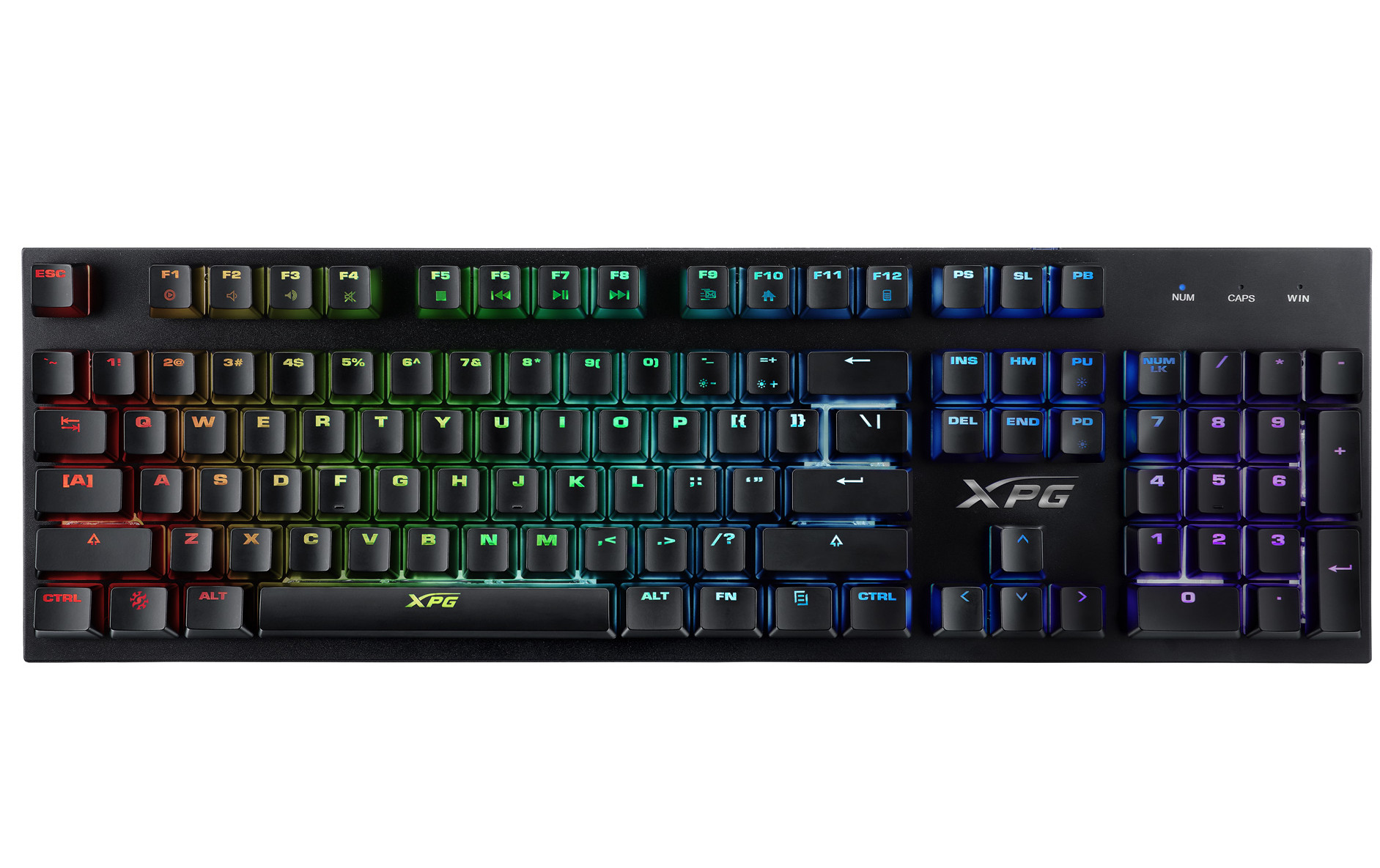
ADATA Launches XPG INFAREX K10 Keyboard and M20 Mouse
ADATA Technology, a leading manufacturer of high-performance DRAM modules and NAND Flash products, today announced the launch of two new gaming accessories, the XPG INFAREX K10 keyboard, and M20 mouse. Designed to enhance gaming experiences, the K10 keyboard sports nine LED lighting modes, anti-ghosting keys, and ergonomic keycaps, while the M20 mouse features durable OMRON switches, five-setting adjustable DPI, and RGB lighting.
The XPG K10 adds a new dimension to gaming with nine stunning LED lighting modes to choose from, allowing gamers to select the hue that best suits the games they are playing. The modes include - Flowing Light, Multicolor Breathing, Seven-Color Cycle Flickering, Switchable Static, Six-Color Cycle Breathing, Red and White Breathing Cycle, Red and White Cycle Flickering, White Static, and White Breathing. What's more, the K10 helps gamers up their game with some great features including 26 anti-ghosting keys to prevent missed or accidental keypresses, because in the heat of the moment a missed keypress could spell defeat. In combination with its ergonomically curved keycaps, the K10 improves accuracy, while also offering a comfortable keypress experience. Convenient Media Keys allow for quick adjustments of music, sound, or other effects in the middle of a battle without having to open other programs or app.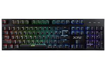

The XPG K10 adds a new dimension to gaming with nine stunning LED lighting modes to choose from, allowing gamers to select the hue that best suits the games they are playing. The modes include - Flowing Light, Multicolor Breathing, Seven-Color Cycle Flickering, Switchable Static, Six-Color Cycle Breathing, Red and White Breathing Cycle, Red and White Cycle Flickering, White Static, and White Breathing. What's more, the K10 helps gamers up their game with some great features including 26 anti-ghosting keys to prevent missed or accidental keypresses, because in the heat of the moment a missed keypress could spell defeat. In combination with its ergonomically curved keycaps, the K10 improves accuracy, while also offering a comfortable keypress experience. Convenient Media Keys allow for quick adjustments of music, sound, or other effects in the middle of a battle without having to open other programs or app.


NVIDIA Unveils Tesla K80 Dual-Chip Compute Accelerator
NVIDIA today unveiled a new addition to the NVIDIA Tesla Accelerated Computing Platform: the Tesla K80 dual-GPU accelerator, the world's highest performance accelerator designed for a wide range of machine learning, data analytics, scientific, and high performance computing (HPC) applications.
The Tesla K80 dual-GPU is the new flagship offering of the Tesla Accelerated Computing Platform, the leading platform for accelerating data analytics and scientific computing. It combines the world's fastest GPU accelerators, the widely used CUDA parallel computing model, and a comprehensive ecosystem of software developers, software vendors, and datacenter system OEMs.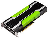
The Tesla K80 dual-GPU is the new flagship offering of the Tesla Accelerated Computing Platform, the leading platform for accelerating data analytics and scientific computing. It combines the world's fastest GPU accelerators, the widely used CUDA parallel computing model, and a comprehensive ecosystem of software developers, software vendors, and datacenter system OEMs.


AMD Sued for Overestimating APU Success to Investors
Some investors in AMD, who purchased company stock between October 27, 2011 and October 18, 2012, filed a class action lawsuit against AMD, through law firm Robbins Geller Rudman & Dowd. The class action alleges that AMD and its officers and directors committed violations of the US Securities Exchange Act of 1934. AMD allegedly misled its investors over how popular its first generation "Llano" desktop APU would get, claiming that there were much greater prospects for the APU than it actually ended up selling.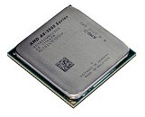
AMD Rolls Out Athlon II X2 280 Value Dual-Core Processor
It's not retirement time for AMD's 45 nm "Regor" silicon just yet, with the company announcing the Athlon II X2 280 value dual-core processor. Built in the socket AM3 package (compatible with AM2/AM2+/AM3/AM3+ motherboards), and based on the company's K10.5 micro-architecture, the chip features two x86-64 cores clocked at 3.60 GHz, 1 MB of L2 cache per core (2 MB total), an instruction set that includes SSE3 and SSE4A, and a dual-channel integrated memory controller that supports both DDR2 and DDR3 memory types. The chip can take advantage of HyperTransport 3.0 interface, with a maximum data-rate of 4.0 GT/s. It features a rated TDP of 65W, and is designed for entry-level desktops. It is priced at US $49.99.
APUs Make Up Nearly 75% of AMD's Processor Sales
Despite losing in market share to Intel, AMD has reason to cheer as its APU gambit is beginning to pay off. According to the latest architecture- and core count-specific sales figures for AMD given out by Mercury Research detailing Q3-2013 in context of two preceding quarters, APUs make for nearly 75% of AMD's processor sales, and the company's recently-launched "Trinity" line of desktop and mobile APUs are off to a flying start.
The most popular chips in AMD's stable are its "Bobcat" Zacate series low-power APUs, which are being built into entry-level computing devices such as netbooks, nettops, and all-in-one desktops. The chips make up 39 percent of AMD's sales in Q3, followed by another APU line, the A-Series "Trinity", which is available in desktop and mobile variants, offers a combination of a fast integrated graphics processor with up to four CPU cores, and makes up 26.1 percent of AMD's sales. AMD's A-Series "Llano" can still be bought in the market, and makes up 7.4 percent of AMD's sales in Q3.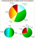
The most popular chips in AMD's stable are its "Bobcat" Zacate series low-power APUs, which are being built into entry-level computing devices such as netbooks, nettops, and all-in-one desktops. The chips make up 39 percent of AMD's sales in Q3, followed by another APU line, the A-Series "Trinity", which is available in desktop and mobile variants, offers a combination of a fast integrated graphics processor with up to four CPU cores, and makes up 26.1 percent of AMD's sales. AMD's A-Series "Llano" can still be bought in the market, and makes up 7.4 percent of AMD's sales in Q3.

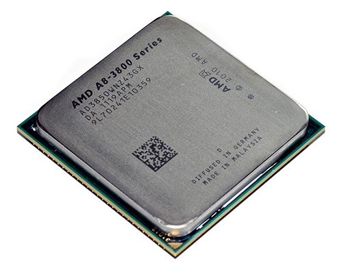
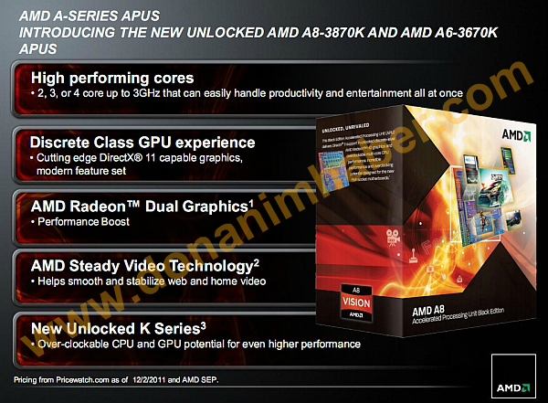
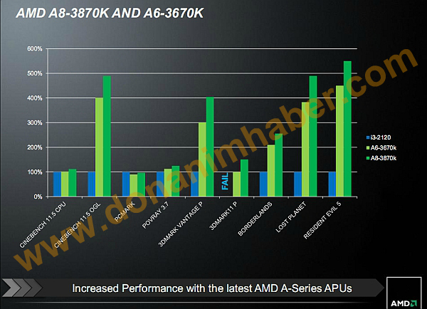
26 December Launch Date for AMD A8-3870K and A6-3670K Black Edition Unlocked APUs
December thru January looks to be a busy time for AMD. Along with a few new graphics products, AMD will launch new CPUs and APUs. The company has chosen December 26 to launch its A8-3870K and A6-3670K Black Edition "Llano" accelerated processing units (APUs) in the FM1 package, which feature unlocked base clock multipliers for the processor component, making overclocking a breeze. In two of its presentation slides to distributors, it unveiled the swanky new box art of these unlocked APUs.
These chips pack four x86-64 cores based on the "Stars" K10.5 architecture with 1 MB dedicated L2 cache per core, dual-channel DDR3-1866 MHz integrated memory controller, PCI-Express 2.0 root complex, and a "discrete-class" graphics processor that packs 400 VLIW5 stream processors, DirectX 11 support, and the ability to pair with similarly specc'd discrete GPUs. The A8-3870K Black Edition features x86 core clock speed of 3.00 GHz, and Radeon HD 6550D graphics that features all 400 of those stream processors, with 600 MHz GPU clock speed. The A6-3670K Black Edition, on the other hand, has its x86 component clocked at 2.70 GHz, it features Radeon HD 6530D graphics that has 320 out of the 400 stream processors enabled, and a GPU clock of 433 MHz.
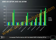
These chips pack four x86-64 cores based on the "Stars" K10.5 architecture with 1 MB dedicated L2 cache per core, dual-channel DDR3-1866 MHz integrated memory controller, PCI-Express 2.0 root complex, and a "discrete-class" graphics processor that packs 400 VLIW5 stream processors, DirectX 11 support, and the ability to pair with similarly specc'd discrete GPUs. The A8-3870K Black Edition features x86 core clock speed of 3.00 GHz, and Radeon HD 6550D graphics that features all 400 of those stream processors, with 600 MHz GPU clock speed. The A6-3670K Black Edition, on the other hand, has its x86 component clocked at 2.70 GHz, it features Radeon HD 6530D graphics that has 320 out of the 400 stream processors enabled, and a GPU clock of 433 MHz.
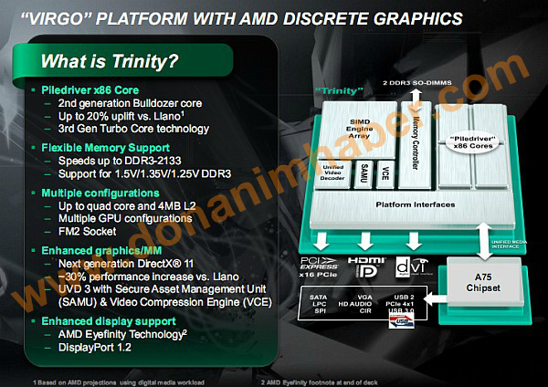
AMD Trinity Detailed Further, Compatible with A75 Chipset
AMD detailed its upcoming "Virgo" PC platform that consists of next-generation "Trinity" APU (accelerated processing unit), and current-generation AMD A75 "Hudson-D" chipset. A notable revelation here is that the next-gen APUs will be compatible with AMD A75, although it will be designed for a new socket called FM2. It remains to be seen if FM1 and FM2 are pin-compatible.
"Trinity" packs four x86-64 cores based on the next-generation "Piledriver" architecture, arranged in two Piledriver modules. A module is a closely-knit group of two cores, with certain shared and dedicated resources. Each Piledriver module has 2 MB of L2 cache shared between the two cores. In all, Trinity, with its two modules, has 4 MB of L2 cache without any L3 cache.
"Trinity" packs four x86-64 cores based on the next-generation "Piledriver" architecture, arranged in two Piledriver modules. A module is a closely-knit group of two cores, with certain shared and dedicated resources. Each Piledriver module has 2 MB of L2 cache shared between the two cores. In all, Trinity, with its two modules, has 4 MB of L2 cache without any L3 cache.
Review Consensus: AMD FX Processor 8150 Underwhelming
It's been in the works for over three years now. That's right, the first we heard of "Bulldozer" as a processor architecture under development was shortly after the launch of "Barcelona" K10 architecture. Granted, it wasn't possible to load close to 2 billion transistors on the silicon fab technology AMD had at the time, but AMD had a clear window over the last year to at least paper-launch the AMD FX. Delays and bad marketing may have cost AMD dearly in shaping up the product for the market.
After drawing a consensus from about 25 reviews (links in Today's Reviews on the front page), it emerges that:
After drawing a consensus from about 25 reviews (links in Today's Reviews on the front page), it emerges that:
- AMD FX-8150 is missing its performance expectations by a fair margin. Not to mention performance gains in its own presentation, these expectations were built up by how AMD was shaping the product to be a full-fledged enthusiast product with significant performance gains over the previous generation
- AMD ill-marketed the FX-8150. Hype is a double-edged sword, and should not be used if you're not confident your offering will live up to at least most of the hype. AMD marketed at least the top-tier FX-8000 series eight-core processors as the second coming of Athlon64 FX.
GeForce BETA Driver Hints At First GeForce 600 Series Models
If not mission-critical stability, GeForce BETA drivers do tend to be great speculation starters. The driver information file packs entries for existing supported GPUs, as well as some future GPUs. GeForce 285 BETA drivers seem to have contained entries for two such future GPUs, marked "NVIDIA GeForce 610M" and "NVIDIA GeForce GT 630M", with identifications of NVIDIA_DEV.1058.01 and NVIDIA_DEV.0DE9.01, respectively.
These new "discoveries" more or less fall in line with an earlier report of NVIDIA having taped out its first GeForce Kepler family GPU, the GK107. It is becoming clear that NVIDIA has charted out a bottom-up course for its next GPU family, to play safe with the new 28 nm fabrication processes at TSMC, that of beginning with the simplest GPUs, and then scaling them up till the highest-performing part is perfected.
These new "discoveries" more or less fall in line with an earlier report of NVIDIA having taped out its first GeForce Kepler family GPU, the GK107. It is becoming clear that NVIDIA has charted out a bottom-up course for its next GPU family, to play safe with the new 28 nm fabrication processes at TSMC, that of beginning with the simplest GPUs, and then scaling them up till the highest-performing part is perfected.
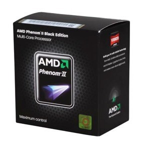
AMD Intros Phenom II X4 980 Black Edition Quad-Core Processor
Today AMD released to market its latest quad-core processor, the Pheonom II X4 980 Black Edition. The new, faster SKU was first reported to be taking shape back in March. Based on the 45 nm "Deneb" silicon and K10.5 architecture, the X4 980 BE is yet another speed-bump, clocked at 3.70 GHz (18.5 x 200 MHz), with room for some overclocking thanks to its unlocked BClk multiplier.
The Deneb die packs four x86-64 cores with 512 KB caches each, and a shared 6 MB L3 cache. Despite its high clock speed, the processor maintains TDP of 125W. Its IMC supports dual-channel DDR3/DDR2 memory, and is backwards compatible with AM2+ socket apart from its native AM3 socket. HyperTransport 4 GT/s is its chipset interconnect. The new processor is priced at US $195.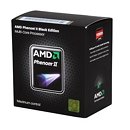
The Deneb die packs four x86-64 cores with 512 KB caches each, and a shared 6 MB L3 cache. Despite its high clock speed, the processor maintains TDP of 125W. Its IMC supports dual-channel DDR3/DDR2 memory, and is backwards compatible with AM2+ socket apart from its native AM3 socket. HyperTransport 4 GT/s is its chipset interconnect. The new processor is priced at US $195.
AMD Orochi ''Bulldozer'' Die Holds 16 MB Cache
Documents related to the "Orochi" 8-core processor by AMD based on its next-generation Bulldozer architecture reveal its cache hierarchy that comes as a bit of a surprise. Earlier this month, at a GlobalFoundries hosted conference, AMD displayed the first die-shot of the Orochi die, which legibly showed key features including the four Bulldozer modules which hold two cores each, and large L2 caches. In coarse visual inspection, the L2 cache of each module seems to cover 35% of its area. L3 cache is located along the center of the die. The documents seen by X-bit Labs reveal that each Bulldozer module has its own 2 MB L2 cache shared between two cores, and an L3 cache shared between all four modules (8 cores) of 8 MB.
This takes the total cache count of Orochi all the way up to 16 MB. This hierarchy suggests that AMD wants to give individual cores access to a large amount of faster cache (that's a whopping 2048 KB compared to 512 KB per core on Phenom, and 256 KB per core on Core i7), which facilitates faster inter-core, intra-module communication. Inter-module communication is enhanced by the 8 MB L3 cache. Compared to the current "Istanbul" six-core K10-based die, that's a 77% increase in cache amount for a 33% core count increase, 300% increase in L2 cache per core. Orochi is built on a 32 nm GlobalFoundries process, it is sure to have a very high transistor count.
This takes the total cache count of Orochi all the way up to 16 MB. This hierarchy suggests that AMD wants to give individual cores access to a large amount of faster cache (that's a whopping 2048 KB compared to 512 KB per core on Phenom, and 256 KB per core on Core i7), which facilitates faster inter-core, intra-module communication. Inter-module communication is enhanced by the 8 MB L3 cache. Compared to the current "Istanbul" six-core K10-based die, that's a 77% increase in cache amount for a 33% core count increase, 300% increase in L2 cache per core. Orochi is built on a 32 nm GlobalFoundries process, it is sure to have a very high transistor count.
Bulldozer-based Orochi and Fusion Llano Die Shots Surface in GlobalFoundaries Event
The first official die-shots of the first Bulldozer architecture derivative, the eight-core "Orochi" Opteron die was displayed at Global Technology Conference, by GlobalFoundries, AMD's principal foundry-partner. While AMD did not give out a die-map to go with it, the structures we can make out are four Bulldozer modules holding two cores and a shared L2 cache each, a L3 cache spread across four blocks that's shared between all cores, the northbridge-portion cutting across the die at the center, and the integrated memory controller along its far-right side. Various I/O portions are located along the other three sides.
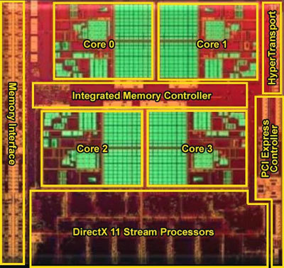
Next up is the Llano die. This is AMD's very first Fusion APU (accelerated processing unit) die. It is based on the K10 architecture and integrates a graphics processor and northbridge completely into one die. It precedes APUs based on the Bobcat architecture. Fortunately, there is a die-map at hand, which shows four K10 cores with dedicated 1 MB L2 caches per core, no L3 cache, an integrated SIMD array that holds 480 stream processors. The GPU component is DirectX 11 compliant. Other components include an integrated northbridge, integrated memory controller, integrated PCI-Express root complex, and HyperTransport interface to the chipset.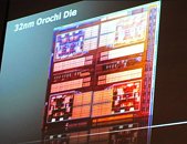
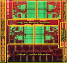
Next up is the Llano die. This is AMD's very first Fusion APU (accelerated processing unit) die. It is based on the K10 architecture and integrates a graphics processor and northbridge completely into one die. It precedes APUs based on the Bobcat architecture. Fortunately, there is a die-map at hand, which shows four K10 cores with dedicated 1 MB L2 caches per core, no L3 cache, an integrated SIMD array that holds 480 stream processors. The GPU component is DirectX 11 compliant. Other components include an integrated northbridge, integrated memory controller, integrated PCI-Express root complex, and HyperTransport interface to the chipset.

AMD Details Bulldozer Processor Architecture
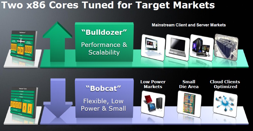
AMD is finally going to embrace a truly next generation x86 processor architecture that is built from ground up. AMD's current architecture, the K10(.5) "Stars" is an evolution of the more market-successful K8 architecture, but it didn't face the kind of market success as it was overshadowed by competing Intel architectures. AMD codenamed its latest design "Bulldozer", and it features an x86 core design that is radically different from anything we've seen from either processor giants. With this design, AMD thinks it can outdo both HyperThreading and Multi-Core approaches to parallelism, in one shot, as well as "bulldoze" through serial workloads with a broad 8 integer pipeline per core, (compared to 3 on K10, and 4 on Westmere). Two almost-individual blocks of integer processing units share a common floating point unit with two 128-bit FMACs.
AMD is also working on a multi-threading technology of its own to rival Intel's HyperThreading, that exploits Bulldozer's branched integer processing backed by shared floating point design, which AMD believes to be so efficient, that each SMT worker thread can be deemed a core in its own merit, and further be backed by competing threads per "core". AMD is working on another micro-architecture codenamed "Bobcat", which is a downscale implementation of Bulldozer, with which it will take on low-power and high performance per Watt segments that extend from all-in-One PCs all the way down to hand-held devices and 8-inch tablets. We will explore the Bulldozer architecture in some detail.
AMD is also working on a multi-threading technology of its own to rival Intel's HyperThreading, that exploits Bulldozer's branched integer processing backed by shared floating point design, which AMD believes to be so efficient, that each SMT worker thread can be deemed a core in its own merit, and further be backed by competing threads per "core". AMD is working on another micro-architecture codenamed "Bobcat", which is a downscale implementation of Bulldozer, with which it will take on low-power and high performance per Watt segments that extend from all-in-One PCs all the way down to hand-held devices and 8-inch tablets. We will explore the Bulldozer architecture in some detail.

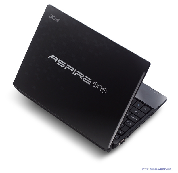
Acer Designs Aspire One Netbook With Low-Wattage AMD Processor
Acer is expanding its Aspire One line of netbooks with an interesting new addition that features a yet to be announced AMD processor with an incredibly low TDP by AMD's standards. The Aspire One 521 features an AMD V105 "Geneva" single-core processor with a TDP of 9W, which operates at 1.2 GHz, which is expected to be based on the AMD K10 architecture. The 10.1 inch netbook has DDR3 memory, integrated ATI Radeon HD 4225 graphics, and connectivity which includes Bluetooth 3.0, WiFi, and gigabit Ethernet. Its battery can power the machine for 7 hours. More information is expected soon.
Phenom II X6 Series Details Surface, Slated for May 2010
AMD's upcoming six-core desktop processor, codenamed "Thuban" is on course for a May 2010, suggests a report. The series is likely to receive the brand name Phenom II X6. There are four models planned for release within Q2, 2010. The Thuban core is AMD's desktop implementation of the Istanbul core, in the socket AM3 package, supporting dual-channel DDR3 memory. It is a monolithic multi-core design with six x86-64 cores, each with 128 KB of L1, 512 KB of L2 cache, and a 6 MB L3 cache shared between the six cores. Just as with K10 dual, triple, and quad core processors where AMD used a HyperTransport interface clock speed of 1800 MHz (3600 MT/s), or 2000 MHz (4000 MT/s), the new processor will take advantage of HyperTransport 3.x interface, with a HT speed of 2400 MHz (4800 MT/s). Thuban will be built on GlobalFoundaries' 45 nm node.
The table below lists out details of the four planned models. The model number of the top part isn't known. Most likely it is a Black Edition part, which comes with an unlocked BClk multiplier. It operates at 2.80 GHz, with a TDP of 140W. A step below is the Phenom II X6 1075T, which has an expected TDP of 125W, the 1055T is a notch below, and 1035T being the cheapest part. The exact clock speeds of the latter three models isn't known as yet. A month ahead of releasing these chips, AMD will announce the AMD 8-series chipset platform, led by 890FX (high-end, best for CrossFireX), 890GX (performance integrated graphics with CrossFire support). The AMD SB800 series southbridge chips will feature native support for SATA 6 Gb/s. Its on-die SATA controller gives out six SATA ports complete with RAID support. Some existing AM3 motherboards based on 7-series chipsets may also support Phenom II X6 with a BIOS update.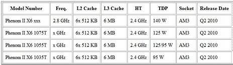
The table below lists out details of the four planned models. The model number of the top part isn't known. Most likely it is a Black Edition part, which comes with an unlocked BClk multiplier. It operates at 2.80 GHz, with a TDP of 140W. A step below is the Phenom II X6 1075T, which has an expected TDP of 125W, the 1055T is a notch below, and 1035T being the cheapest part. The exact clock speeds of the latter three models isn't known as yet. A month ahead of releasing these chips, AMD will announce the AMD 8-series chipset platform, led by 890FX (high-end, best for CrossFireX), 890GX (performance integrated graphics with CrossFire support). The AMD SB800 series southbridge chips will feature native support for SATA 6 Gb/s. Its on-die SATA controller gives out six SATA ports complete with RAID support. Some existing AM3 motherboards based on 7-series chipsets may also support Phenom II X6 with a BIOS update.

AMD SSE5 Gets an Instruction-Set Expansion, Coins XOP (eXtended Operations)
AMD kept up with the SIMD processing standards Intel set by licensing its popular CPU instruction sets such as MMX, SSE, SSE2, and SSE3. The three were used as is by AMD, except for that AMD chose not to conform completely with Supplemental SSE3, SSE4 and its revisions (SSE4.1, SSE4.2). The company devised the SSE4A instruction set to feature with its K10 micro-architecture. SSE4A is a lighter version that features LZCNT (Leading Zero Count), POPCNT (bit population count), EXTRQ/INSERTQ and MOVNTSD/MOVNTSS (Scalar streaming store instructions). What's more, the company even decided back in 2007 that it would come up with SSE5, that then Intel sought to leave development with AMD.
In due course of time, Intel started development of AVX (Advanced Vector eXtensions) that enhances processing of FPU-intensive workloads. AMD gained interest in this technology, and is looking to make it compatible with the originally-conceived SSE5. The instructions that remain as part of the superset that doesn't include AVX is now referred to by AMD as XOP (eXtended OPerations). In addition to this, AMD will include FMA4 (Floating point vector Multiply-Accumulate). The new instruction sets make it to AMD's next-generation Bulldozer micro-architecture slated for 2011. Meanwhile, Intel's AVX makes it to the Sandy Bridge micro-architecture slated for 2010~11. AMD published the Programmer's Manual document on 128-Bit and 256-Bit XOP, FMA4 and CVT16 Instructions, which can be read here (PDF).
In due course of time, Intel started development of AVX (Advanced Vector eXtensions) that enhances processing of FPU-intensive workloads. AMD gained interest in this technology, and is looking to make it compatible with the originally-conceived SSE5. The instructions that remain as part of the superset that doesn't include AVX is now referred to by AMD as XOP (eXtended OPerations). In addition to this, AMD will include FMA4 (Floating point vector Multiply-Accumulate). The new instruction sets make it to AMD's next-generation Bulldozer micro-architecture slated for 2011. Meanwhile, Intel's AVX makes it to the Sandy Bridge micro-architecture slated for 2010~11. AMD published the Programmer's Manual document on 128-Bit and 256-Bit XOP, FMA4 and CVT16 Instructions, which can be read here (PDF).
Athlon X2 7000 Series Reviewed
AMD is releasing a trio of dual-core desktop processors based on the K10 architecture, under the Athlon X2 7000 series. The trio consists of the overclocker-friendly 7750 Black Edition clocked at 2.70 GHz, the 7550 at 2.50 GHz and the 7450 at 2.40 GHz. The core, codenamed "Kuma" sports a basic cache design similar to the Phenom X3 and Phenom X4 processors, with 512 KB of L2 caches per core, and a shared L3 cache of 2 MB. The updated memory controller provides native support to the PC2-8500 (DDR2 1066 MHz) memory standard. The processor now sports a HyperTransport 3.0 3600 MT/s system interface. These, apart from the other tweaks AMD introduced with the K10 architecture give it an edge over current K8 based dual core AMD chips. The core is manufactured in the 65nm node.
AMD lifted the NDA over the Athlon X2 7000 series, following which several website posted reviews on the processors. Most of these reviews covered the Athlon X2 7750 Black Edition. The chip clocked at 2.7 GHz was found to be around 15% faster than a previous-generation Brisbane chip running at the same frequency, according to X-bit Labs, whose evaluation included several synthetic and real-world benchmarks. The same review team was able to overclock the chip to 3.30 GHz (+22 %) aided by a Zalman 9700 air cooler. The Athlon X2 7750 Black Edition will be priced at US $79. Links to some of the reviews are provided below.
Bit-Tech | Hexus | HT4U | Overclockers Club | Planet 3DNow! | Tweaktown | X-bit Labs
AMD Shanghai Ready to Ship
AMD Shanghai is the codename for a new enterprise processor the company is working on. It is a monolithic quad-core x86 processor that retains the design methodology of the K10h generation of AMD processors. It carries forward the Opteron brand. This time around, the company promises to have made numerous changes, big and small, learning from the shortfalls of the Barcelona chip. Shanghai will be the first 45nm AMD processor to make it to the market. Originally slated for Q1, 2009 its launch was pushed to Q4, 2008.
In a press event held yesterday, the company claimed that the company is all set to roll out the new chip. Initial volumes of the processor would run off existing core logic platforms by NVIDIA and Broadcom. It will retain the Socket F (aka s1207) package and support DDR2 memory. The lineup shows that most of these chips would retain the 2000 MT/s system bus, and all of them come with 6 MB of level 3 cache. A new company slide sourced by C|Net shows that the Opteron processor could embrace DDR3 memory only by 2010, with the introduction of the Magny-Corus 12-core processor architecture. Until then, the Istanbul 6-core processor the is slated for H2, 2009, could be the company's flagship product.
In a press event held yesterday, the company claimed that the company is all set to roll out the new chip. Initial volumes of the processor would run off existing core logic platforms by NVIDIA and Broadcom. It will retain the Socket F (aka s1207) package and support DDR2 memory. The lineup shows that most of these chips would retain the 2000 MT/s system bus, and all of them come with 6 MB of level 3 cache. A new company slide sourced by C|Net shows that the Opteron processor could embrace DDR3 memory only by 2010, with the introduction of the Magny-Corus 12-core processor architecture. Until then, the Istanbul 6-core processor the is slated for H2, 2009, could be the company's flagship product.


Phenom X4, X3 45nm Lineup for H1 2009 Explained
AMD would be releasing its first desktop processors based on the 45nm silicon fabrication process, based on the newer Deneb core. The company is said to have made several tweaks to the original K10 design and equipped the core with 300% the amount of L3 cache as its 65nm Agena parts. The only thing got us wondering was what would be its nomenclature like? Well, be surprised to know that after Phenom X4 9000 series, the company plans to continue the numbering with a 5-digit model number scheme with x1000 unit deviations between models. A rather confusing naming scheme, as suggested by the chart provided, seems to have been adopted.
It is now clear, that there will be two distinct kinds of Phenom X4 45nm chips: those which continue support for DDR2 memory on the existing AM2/AM2+ sockets, and those which are exclusive to the AM3 socket and feature support for DDR3 memory, DDR3 1333MHz at that. The processors would feature dual 64-bit memory controllers, which could be ganged for a single 128-bit wide memory interface, or un-ganged to step up multi-tasking efficiency.
It is now clear, that there will be two distinct kinds of Phenom X4 45nm chips: those which continue support for DDR2 memory on the existing AM2/AM2+ sockets, and those which are exclusive to the AM3 socket and feature support for DDR3 memory, DDR3 1333MHz at that. The processors would feature dual 64-bit memory controllers, which could be ganged for a single 128-bit wide memory interface, or un-ganged to step up multi-tasking efficiency.

Phenom X2 Churns out Roughly 15% Increments with Super Pi
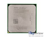
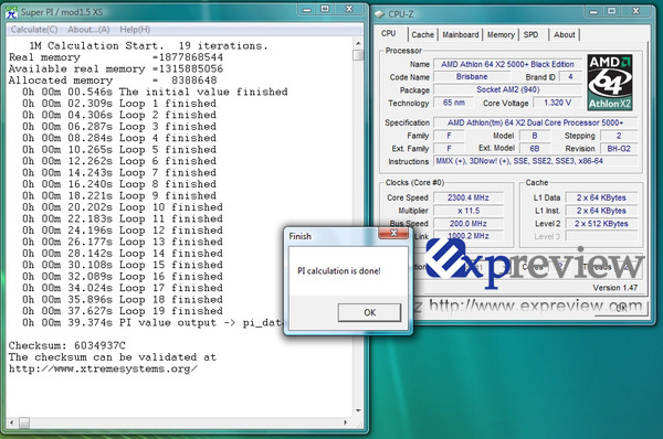
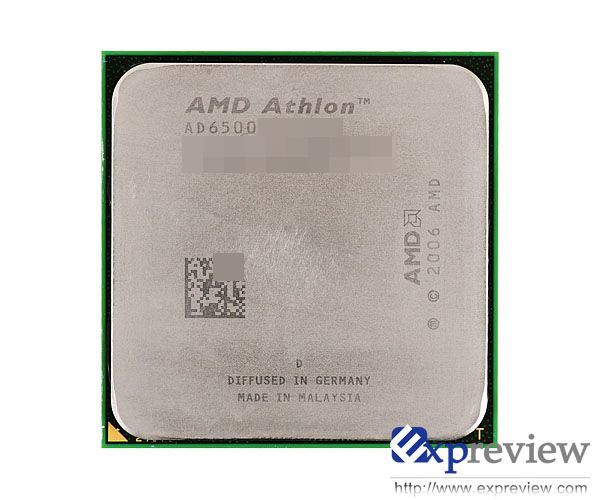
Phenom X2 is intended to be the latest dual-core processor from AMD. It is based on the newer K10 architecture. The 65nm Kuma core is what sits inside the first to release models of the Phenom X2. Although based on K10 architecture and Kuma core, the initial batch being 65nm, AMD for some reason chooses to call it Athlon X2 saving the Phenom brand name perhaps for the 45nm batches? At least the sample Expreview got had the Athlon X2 etching on it. The chip carried the "AD6500" label and came with a 2.30 GHz clock speed.
Here's something to ponder: 6500 isn't a performance rating, it is just a model number. The Athlon 64 X2 6400+ had a 3.20 GHz clock speed. As performance evaluations will soon show, the Phenom/Athlon 6500 isn't anywhere close to the performance of the X2 6400+. However, architectural improvements meant that Kuma outperforms Brisbane (K8, 65nm) on a clock to clock basis. To ascertain this, Expreview used a Athlon 64 X2 5000+ Black Edition (Brisbane) that was underclocked to 2.30 GHz, the clock speed which AD6500 comes with. Super Pi 1M benchmark was run. While the Brisbane chip crunched it in 39.374 s, Kuma did it in 33.43 s indicating a performance increment of roughly 15%. The test-bed consisted of a NVIDIA nForce 750a SLI motherboard and GEIL 1GB DDR2-800 memory. Kuma AD6500 comes with a shared L3 cache of 2 MB apart from dedicated L2 caches of 512 KB per core. It uses a broader HyperTransport 3.0 system interface at 3600 MT/s. It supports DDR2-1066.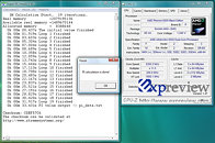
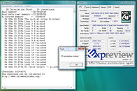
Here's something to ponder: 6500 isn't a performance rating, it is just a model number. The Athlon 64 X2 6400+ had a 3.20 GHz clock speed. As performance evaluations will soon show, the Phenom/Athlon 6500 isn't anywhere close to the performance of the X2 6400+. However, architectural improvements meant that Kuma outperforms Brisbane (K8, 65nm) on a clock to clock basis. To ascertain this, Expreview used a Athlon 64 X2 5000+ Black Edition (Brisbane) that was underclocked to 2.30 GHz, the clock speed which AD6500 comes with. Super Pi 1M benchmark was run. While the Brisbane chip crunched it in 39.374 s, Kuma did it in 33.43 s indicating a performance increment of roughly 15%. The test-bed consisted of a NVIDIA nForce 750a SLI motherboard and GEIL 1GB DDR2-800 memory. Kuma AD6500 comes with a shared L3 cache of 2 MB apart from dedicated L2 caches of 512 KB per core. It uses a broader HyperTransport 3.0 system interface at 3600 MT/s. It supports DDR2-1066.

AMD Desktop Roadmap for 2009 Reveals no Surprises
Without doubt, AMD needs something revolutionary to pull it out of the mess it set itself in. AMD's first reaction to the Conroe onslaught was to lower prices and build up a "Smarter Choice" repute, though with successive price cuts from Intel and down-scale products based on the Core architecture coming out by the fortnight, and the transit to 45nm fab process, there's been an increasing need for AMD to get back to the drawing boards with their CPU division.
From what looks like an excerpt from an AMD company slide, can be seen AMD's CPU plans for 2009. The chart broadly shows that K10 architecture is here to stay. Throughout the year, desktop CPUs based on the K10 architecture feature in the roadmap, with no signs of their "truly next-gen" architecture. AMD completes its transit to the 45nm silicon fabrication process and will finally embrace DDR3 system memory standards. To begin with, the fact that the Deneb core's entry slightly steps into the 2008 column shows that the Deneb core-based desktop CPU could release sometime towards the very end of this year. Sources note that two models based on the Deneb core could be out by the end of this year. It supports both DDR2 and DDR3 memory standards and socket compatible with current AM2+ and future AM3. From what's known so far, AM3 is the same 940 pin design that adds pins for the DDR3 memory interconnect between the CPU and the memory.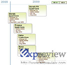
From what looks like an excerpt from an AMD company slide, can be seen AMD's CPU plans for 2009. The chart broadly shows that K10 architecture is here to stay. Throughout the year, desktop CPUs based on the K10 architecture feature in the roadmap, with no signs of their "truly next-gen" architecture. AMD completes its transit to the 45nm silicon fabrication process and will finally embrace DDR3 system memory standards. To begin with, the fact that the Deneb core's entry slightly steps into the 2008 column shows that the Deneb core-based desktop CPU could release sometime towards the very end of this year. Sources note that two models based on the Deneb core could be out by the end of this year. It supports both DDR2 and DDR3 memory standards and socket compatible with current AM2+ and future AM3. From what's known so far, AM3 is the same 940 pin design that adds pins for the DDR3 memory interconnect between the CPU and the memory.

AMD Phenom X2 Information Trickles
Time draws closer for the Athlon 64 X2 to retire. It has seen its good and bad days, leading Intel versus the Pentium D and trailing it versus the Core 2 Duo. German site Hardware Infos shed light on the primary lineup of the dual-core edition based on the K10 architecture, the Phenom X2. There are no core architectural changes for the Phenom X2, codenamed "Kuma" over the K8, except that like the Phenom X3 and X4, these chips feature 2 MB of L3 cache apart from 512 KB caches per core and the revised HyperTransport interface. The listed models come at a rated TDP of 45W. The first three Kuma chips listed have clock-speeds ranging from 1.90 GHz to 2.30 GHz and have been given model numbers that look confusing to the older PRN system AMD employed, with the top Athlon 64 X2 rated at 6400+. The later releases of the older X2 using the Brisbane core broke away from the older PRN and we saw models such as 4450e, 4850e or 4850b (note the absence of the "+").
The naming of these chips asserts that. For example, the 1.90 GHz Kuma part is named Phenom X2 GE-6400. Going by the performance evaluations of other parts based on the K10 architecture, at 1.90 GHz + the 2 MB L3 cache, this part might not be on par with the Windsor core Athlon 64 X2 6400+. Contradicting earlier reports that AMD would work out Kuma parts on the 45 nm fabrication process, all three Kuma parts reported are based on the 65 nm fab process.
The naming of these chips asserts that. For example, the 1.90 GHz Kuma part is named Phenom X2 GE-6400. Going by the performance evaluations of other parts based on the K10 architecture, at 1.90 GHz + the 2 MB L3 cache, this part might not be on par with the Windsor core Athlon 64 X2 6400+. Contradicting earlier reports that AMD would work out Kuma parts on the 45 nm fabrication process, all three Kuma parts reported are based on the 65 nm fab process.
CPU Errata Turn Security Vulnerabilities
Security vulnerabilities have plagued the computing world ever since computing became a significant advance of mankind. As of today, the plethora of security software we use that gobble money, system resources and network bandwidth to keep our computers and networks safe, have done a good job and it's relatively 'peaceful' these days. And just when we thought so, enter Kris Kaspersky, eminent security researcher, comes up with the hypothesis that microcode errors, known errors and flaws in the design of CPUs could be exploited by malicious code to attack and compromise systems irrespective of which operating system (OS) and other software are running. Kaspersky claims that different errata of the CPU could be exploited differently.
Apr 16th, 2025 08:52 EDT
change timezone
Latest GPU Drivers
New Forum Posts
- Last game you purchased? (771)
- GPU Memory Temprature is always high (16)
- Windows 11 fresh install to do list (20)
- 5070ti overclock...what are your settings? (3)
- Help For XFX RX 590 GME Chinese - Vbios (4)
- PCGH: "hidden site" to see total money spend on steam (3)
- Share your AIDA 64 cache and memory benchmark here (3053)
- NVFlash for RTX 50 Series (Blackwell) (0)
- intel 1700 with high speed ram,memory (63)
- The TPU UK Clubhouse (26115)
Popular Reviews
- G.SKILL Trident Z5 NEO RGB DDR5-6000 32 GB CL26 Review - AMD EXPO
- ASUS GeForce RTX 5080 TUF OC Review
- DAREU A950 Wing Review
- The Last Of Us Part 2 Performance Benchmark Review - 30 GPUs Compared
- Sapphire Radeon RX 9070 XT Pulse Review
- Sapphire Radeon RX 9070 XT Nitro+ Review - Beating NVIDIA
- Upcoming Hardware Launches 2025 (Updated Apr 2025)
- Thermaltake TR100 Review
- Zotac GeForce RTX 5070 Ti Amp Extreme Review
- TerraMaster F8 SSD Plus Review - Compact and quiet
Controversial News Posts
- NVIDIA GeForce RTX 5060 Ti 16 GB SKU Likely Launching at $499, According to Supply Chain Leak (182)
- NVIDIA Sends MSRP Numbers to Partners: GeForce RTX 5060 Ti 8 GB at $379, RTX 5060 Ti 16 GB at $429 (124)
- Nintendo Confirms That Switch 2 Joy-Cons Will Not Utilize Hall Effect Stick Technology (105)
- Over 200,000 Sold Radeon RX 9070 and RX 9070 XT GPUs? AMD Says No Number was Given (100)
- Nintendo Switch 2 Launches June 5 at $449.99 with New Hardware and Games (99)
- Sony Increases the PS5 Pricing in EMEA and ANZ by Around 25 Percent (85)
- NVIDIA PhysX and Flow Made Fully Open-Source (77)
- NVIDIA Pushes GeForce RTX 5060 Ti Launch to Mid-April, RTX 5060 to May (77)