News Posts matching #Llano

Return to Keyword Browsing

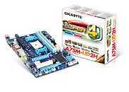
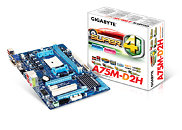
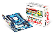
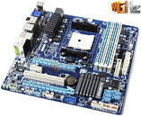
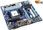
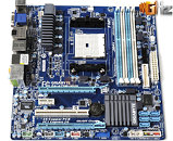
GIGABYTE Rolls Out A75 Motherboards For AMD Llano A8 and A6 APUs

GIGABYTE TECHNOLGY Co. Ltd., a leading manufacturer of motherboards and graphics cards, today launched its latest series of motherboards supporting the new AMD A75 series chipsets, and the latest AMD A-Series APUs (codenamed Llano) that are set to take the world by storm with the best graphics performance ever seen on an onboard graphicsprocessor. GIGABYTE A75 based motherboards offer DIY PC builders and integrators a new world of 3D and multimedia performance with the most scalable, and best value upgrade path imaginable.

"At GIGABYTE, we are delighted to bring to market this new and exciting motherboard range, delivering our renowned durability and exceptional feature support to AMD's ground breaking APU technology," commented Henry Kao, VP of Worldwide Service and Marketing at GIGABYTE. "As well as bringing AMD A-Series technology to DIY users who demand excellent gaming and multimedia performance on a budget, these motherboards also offer a compelling upgrade path that includes Dual Graphics configurations."


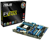
ASUS Announces New F1A75 Series Motherboards

ASUS today announced the launch of their new AMD A75 chipset-based F1A75 Series motherboards. Designed specially to optimize performance for the AMD Llano APUs, the F1A75 Series motherboards have exceptional overclocking capability for the versatile APU with a variety of integrated graphics built directly on the same die. This new series is also equipped with the latest ASUS-exclusive technologies and features, including the Dual Intelligent Processors 2 (DIP2) with DIGI+ VRM for precise power control, a graphical and mouse-controlled UEFI BIOS and the easy-to-use auto tuning for better performance.

BIOSTAR Releases the Most Powerful AMD APU Mainboards

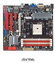
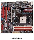
AMD's officially launched the new Llano APU platform for market availability in July worldwide, and BIOSTAR is releasing three mainboards that support this new platform at the same time; the "TA75A+", "TA75M+" and "TA75M". The advantages of the new AMD A75 chipset based motherboard include native support of USB3.0, DX11 graphic core for greater 3D performance, and BIOSTAR exclusive features (BIO-Remote2, Charger Booster, and etc.).

The new AMD A75 chipset series mainboards, "TA75A+", "TA75M+", "TA75M", all using AMD Hudson-D3 A75 single-chip design, "TA75A+" with ATX form factor and the other two are with micro-ATX form factor. With a brand new heat sink design that also gives a better outlook and better thermal efficiency.

AMD Catalyst 11.6 WHQL Driver Suite Released

AMD Catalyst received its monthly major update with version 11.6 WHQL. The driver isn't posted on AMD Game website, but leaked to the media. The new drivers bring support for AMD's new Fusion "Llano" A-series accelerated processing units (APUs), which embed AMD Radeon HD 6000 series GPU components. The new drivers also introduce the new AMD Steady Video Technology, which is an AMD APP-based software that works on AMD Radeon HD 6000 series graphics cards (only on systems that also run AMD processors), AMD E450, AMD E300 APUs, and AMD A8, A6, and A4 series APUs. The technology processes videos for image-stabilization of each frame, giving out a "steady" video output. Videos processed by Steady Video are compatible with any of the popular video players, including Adobe Flash player, Windows Media player, Cyberlink PowerDVD, Corel Win DVD, ArcSoft TotalMedia Theater.

With the new driver, AMD enabled decode acceleration of MPEG-4 part-2 content in Microsoft's video player applications (through MFT support) for all AMD Radeon 6000 Series GPUs. The new driver also packs a number of game-specific performance enhancements, for applications such as Dirt 2, F1 2010, Tom Clancy's HAWX, Crysis Warhead, and Unigine Heaven (OpenGL). For more information, refer to the Release Notes article.

AMD Ushers in Next Generation of Computing with AMD A-Series APUs

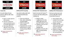
AMD today announced the next generation in mainstream consumer computing with the availability of the new high-performance AMD Fusion A-Series Accelerated Processing Units (APUs). Enabling truly immersive computing experiences in consumer notebooks and desktops, the AMD A-Series APUs enable brilliant HD graphics, supercomputer-like performance and over 10.5 hours of battery life.

In an increasingly digital and visually oriented world, consumers are placing ever-higher priorities on multitasking, vivid graphics, lifelike games, lag-free videos, and ultimate multimedia performance. To meet these needs, the AMD A-Series APUs combine up to four x86 CPU cores with powerful DirectX 11-capable discrete-level graphics and up to 400 Radeon cores along with dedicated HD video processing on a single chip. AMD A-Series APUs also allow for advanced capabilities such as gestural interfaces, multi-monitor support, 3D entertainment and real-time image stabilization.

AMD A-Series APU Smashes IGP Performance Records...Surprise

Armed with a Radeon HD 6550D graphics core that has 400 stream processors, 8 ROPs, and full DirectX 11 support, AMD A-Series "Llano" accelerated processing unit (APU) was tested to be the fastest integrated graphics solution to date. The tests was run by a forum-member of TweakTown community with early access to engineering samples. On the test-bed was AMD A8-3850 APU, which has four x86-64 cores clocked at 2.90 GHz, and the Radeon HD 6550D IGP with engine clock of 600 MHz. Standard dual-channel DDR3-1333 MHz memory was used, even though the APU supports faster DDR3-1866 MHz. To seat the test bed, Gigabyte A75M-UD2H was used. It's important to note here that the CPU cores were overclocked to 3.773 GHz (145.13 MHz x 26.0), with an insane core voltage of 1.52V.

The setup was put though three generations of 3DMark benchmark, covering DirectX 9.0c, DirectX 10, and DirectX 11 performance. In 3DMark 06, the setup scores 10,492 points. In 3DMark Vantage, it scored P6160 (performance preset, validation). In 3DMark 11, it scored P1591 (performance preset, validation). More details can be read in the screenshots.

Gigabyte A75M-UD2H Socket FM1 Micro-ATX Motherboard Pictured

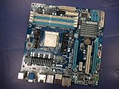
AMD's new Fusion A-Series "Llano" accelerated processing unit (APU) is shaping up to be a credible home and entertainment platform, but it is also carrying the responsibility of making it to office spaces. Part of that initiative would rest with the motherboard manufacturers to come up with inexpensive and durable sub-$100 motherboards that can be bought and deployed in bulk. Enter the Gigabyte A75M-UD2H. This micro-ATX form-factor motherboard relies entirely on the platform's feature-set.

The FM1 APU socket is powered by a simple 4+1 phase VRM, it is wired to four DDR3 DIMM slots supporting dual-channel DDR3-1600 MHz memory. Of the four expansion slots, there's one PCI-Express 2.0 x16, a PCI-E x16 that's electrical x4, and one each of PCI-E x1 and legacy PCI. To further make for its business PC outlook, there are headers for legacy ports such as LPT and COM (for dot-matrix printers in banks, etc.).

AMD Bulldozer, Llano Pricing Surface

Here are the first figures made public of the market prices of AMD's upcoming two lines of desktop processors. AMD will approach the desktop PC market with two platforms, the A-Series "Llano" accelerated processing units (APUs), and the FX-series "Zambezi" processors (CPUs). APUs are functionally similar to Intel's Sandy Bridge processors, in having processor cores, a graphics processor, memory controller, and PCI-Express switch packed into a single piece of silicon. AMD is apparently relying on its powerful GPU architecture to make Llano a more wholesome product. Zambezi functionally resembles Intel Westmere/Bloomfield, in having a number of processing cores, a high-bandwidth memory controller, and a large cache packed into a single die, making up for a performance part.

By mid-June, AMD will launch the FX-Series with two a 4-core, a 6-core, and two 8-core parts. The series will be led by eight-core AMD FX-8130P priced at US $320, trailed by FX-8130 at US $290. The former probably is a "unlocked" part. Next up is the six-core FX-6110, priced at $240. Lastly there's the quad-core FX-4110, going for $220. You will notice that the price per core isn't as linear as it was in the previous generation.

AMD's Fastest Mobile Fusion Processor Detailed

One of AMD's design goals for its Fusion architecture must have been its application in mobile processors, where AMD isn't the brightest in terms of energy efficiency. The company's fastest product for the notebook platform is based on the Llano silicon, will release in 2011, and is a quad-core APU. Enter the AMD A8-3530MX.

Built on the 32 nm process with FS1 package, the A8-3530MX is an accelerated processing unit (APU), it combines a quad-core processor with a powerful GPU and northbridge component. With a default clock speed of 1.90 GHz and TurboCore speed of 2.60 GHz, the A8-3530MX packs 4 MB of L2 cache, and a dual-channel DDR3-1600 MHz memory controller, that also supports DDR3L-1333 MHz.

The GPU component is the DirectX 11 compliant AMD Radeon HD 6620G, with 400 stream processors, and engine clock speed of 444 MHz. To drive it, the northbridge component is entirely integrated into the APU, which packs a PCI-Express 2.0 hub to support discrete graphics. Despite so much machinery, the top-of-the-line chip maintains a TDP of 45W (common for notebook quad-core chips).

AMD FX Series and A Series First Performance Projections Surface

Here are the first performance projections of the AMD FX-series processors. FX-series is the market name of the latest line of 8-core, 6-core, and 4-core processors by AMD, based on its new Bulldozer architecture. The performance projections come from AMD's internal presentations to its industry partners, which was leaked to sections of the media.

In the performance projection, a compound bar graph, an AMD platform comprising of an 8-core FX series processor (unknown model, clock speed) with AMD Radeon HD 6670 discrete graphics, was pitted against its main competitor, Intel Core i7-2600K with its integrated Intel HD graphics. Perhaps AMD is suggesting that FX 8-core model used here along with a HD 6690 graphics card costs the same as a Core i7-2600K.

AMD A-Series APU and FX-Series CPU Launch Schedule Detailed

AMD charted out the launch itinerary of its two upcoming client product lines, the A-Series "Llano" accelerated processing unit (APU), and the FX-Series "Zambezi" processor, in a presentation slide to its launch partners. The series of product launches starts at the upcoming Computex 2011 event, on June 1, where AMD will launch its new 9-series chipset. This could include two branches: first being the 2-chip chipset that drives Zambezi FX-series processors; and a second single-chip chipset for APUs. The action then shifts to E3 (Electronic Entertainment Expo) a week after Computex. On June 7, AMD will unveil the AM3+ platform, and motherboard vendors across the board are expected to show off their AM3+ motherboards

On 12th June AMD's Llano APU and Sabine platform will be launched for the Asian markets. Around the same time, at the AMD Fusion Developer Summit, AMD will interact with developers to develop software that's tailor made for the Fusion architecture (x86 with increased use of serial computational loads over GPGPU). June 14 2011 is the most important date. Called the AMD 2011 Client Launch Event, this event will be the launchpad for AMD's FX-series processors and A-Series APUs. Sabine platform will launched to the rest of the world's markets.

AMD FM1 Socket, Package Pictured

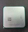
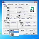
Here are some of the first pictures of AMD's new socket FM1. FM1 will be the platform for AMD's upcoming "Llano" A-Series accelerated processing units (APUs), in the desktop and notebook platforms. With it, AMD will compete with Intel's LGA1155/LGA1156 processors in consumer and business desktop markets that simply rely on the processor's embedded graphics. The Llano APU integrates a quad-core x86-64 processor with a DirectX 11 compliant AMD Radeon HD 6000 series graphics core (with 400+ stream processors, last we heard); a dual-channel DDR3 memory controller, and a PCI-Express 2.0 hub. FM1 is a pin-grid array, but its exact pin count isn't known. Purely by the looks of it, FM1 package looks smaller than AM3+. Clearly the version of CPU-Z used in the screenshot doesn't fully support the APU, but it does reveal some information. It's reading the quad-core chip as four single core processors with 1 MB L2 cache each. The processor is clocked at 2.4 GHz. Llano APUs are expected to make landfall in May/June.

TechPowerUp GPU-Z 0.5.1 Released

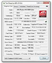
TechPowerUp introduced version 0.5.1 of GPU-Z, our lightweight graphics sub-system information and monitoring utility. GPU-Z provides you with technical details of your installed graphics processors, and lets you monitor clock speeds, voltages, temperatures and fan speeds. This month's release adds support for new GPUs, improves stability, and corrects some minor bugs. To begin with, detection for the new NVIDIA GeForce GTX 560 Ti graphics processor is added, alongside GeForce GTX 480M, and GeForce GTX 485M. Detection was improved for GeForce GTX 460M, GT 445M, and GT 435M. Early support for AMD's Fusion Llano, Ontario, and Zacate-embedded APUs were also added.

With the latest driver, NVIDIA had blocked our power-throttling disable parameter. We found our way around it, and using a new method, fixed the "/GTX500OCP" parameter using which you can override NVIDIA's power throttling feature. Support for new voltage controllers used by the latest batches of Radeon HD 6800/HD 6900 series graphics cards were also added. A number of stability improvements were made, and bugs fixed. The updates notifier is less pesky, it checks for timely updates in the background when GPU-Z is launched (according to update check frequency defined by user), and appears to users only if it finds that new updates are available.

DOWNLOAD: TechPowerUp GPU-Z v0.5.1

A complete list of changes follows.

AMD Details a Vivid Future of Computing at Annual Financial Analyst Day

At its annual Financial Analyst Day, AMD (NYSE: AMD) demonstrated how its unique combination of CPU and GPU computing technologies on a single die will enable breakthrough capabilities in an innovative processor design with planned OEM system availability in early 2011. AMD executives detailed how this new class of processor, AMD Fusion Accelerated Processing Units (APUs), is poised to create a sustained position of advantage by powering demanding PC workloads in sleek form factors with long battery life, pacing future AMD growth. AMD Fusion APUs are built from DirectX 11-capable GPU technology and either low-power or high-performance multi-core x86 CPU technology. These APUs are designed to vastly improve today's Internet, video processing and playback, and gaming (client and online) experiences. For the first time, AMD also demonstrated its new high-performance x86 multi-core CPU architecture codenamed "Bulldozer" and provided additional information around the "Bulldozer" launch schedule.

AMD Fusion APU Codenamed ''Llano'' Demonstrated at 6th Annual AMD TFE 2010

At the 6th Annual AMD Technical Forum & Exhibition (TFE) 2010, AMD today showcased for its ecosystem partners the first public demonstration of the forthcoming AMD Fusion Accelerated Processing Unit (APU) codenamed "Llano", designed for notebook, ultrathin and desktop PCs. AMD demonstrated the accelerated single-chip processing muscle of Llano by simultaneously processing three separate compute-and graphics-intensive workloads.

"The serial and powerful parallel processing capability of the Llano APU has the potential to make OEMs and consumers re-think their computing experience," said Chris Cloran, corporate vice president and general manager, client division, AMD. "The experience potential of Llano is truly incredible, and the demos we showed today on stage provide a glimpse of what this processor is capable of delivering in sleek form factors with long battery life. Everything consumers love about their digital lifestyles today - social networking, gaming, consuming and creating media - can be enhanced with Llano, enabling a more interactive, vivid and immersive experience."

Bulldozer-based Orochi and Fusion Llano Die Shots Surface in GlobalFoundaries Event

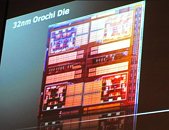
The first official die-shots of the first Bulldozer architecture derivative, the eight-core "Orochi" Opteron die was displayed at Global Technology Conference, by GlobalFoundries, AMD's principal foundry-partner. While AMD did not give out a die-map to go with it, the structures we can make out are four Bulldozer modules holding two cores and a shared L2 cache each, a L3 cache spread across four blocks that's shared between all cores, the northbridge-portion cutting across the die at the center, and the integrated memory controller along its far-right side. Various I/O portions are located along the other three sides.

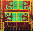
Next up is the Llano die. This is AMD's very first Fusion APU (accelerated processing unit) die. It is based on the K10 architecture and integrates a graphics processor and northbridge completely into one die. It precedes APUs based on the Bobcat architecture. Fortunately, there is a die-map at hand, which shows four K10 cores with dedicated 1 MB L2 caches per core, no L3 cache, an integrated SIMD array that holds 480 stream processors. The GPU component is DirectX 11 compliant. Other components include an integrated northbridge, integrated memory controller, integrated PCI-Express root complex, and HyperTransport interface to the chipset.

AMD Readies New Southbridge Chipset with Native USB 3.0 Support

Although USB 3.0 and SATA 6 Gb/s served as features central to new motherboard models by manufacturers for an entire year, their adoption by chipset vendors has been rather slow. While AMD has integrated SATA 6 Gb/s into its SB850 southbridge, which features a 6-port SATA 6 Gb/s RAID controller, neither Intel nor AMD have USB 3.0 integrated, with no real indication Intel doing so in the foreseeable future. Sources in the motherboard industry, however, reveal that AMD is designing a new southbridge that integrates a USB 3.0 controller, just like present chipsets have USB 2.0.

AMD's move follows a recent announcement of collaboration with Renesas, the company behind the popular NEC uPD720200 controller, to promote USB 3.0 as an industry standard, and a new universal UASP driver model for USB 3.0 controllers. The new southbridge is codenamed "Hudson D1", which will release along with AMD's 40 nm Ontario Fusion APUs in Q4-2010. The company also plans to release the Llano Fusion APU in 2011.

AMD Demonstrates Graphics Processing Power of Llano Fusion APUs

AMD demonstrated its first Fusion APU (accelerated processing unit), which is a "fusion" between a processor and a graphics processor. The first such processor in the works is based on the 32 nm silicon fabrication technology, codenamed Llano, and fuses a quad-core processor with a DirectX 11 compliant GPU. AMD's Rick Bergman showed off a wafer of the Llano APUs, but it didn't stop there. Rick surprised the press when he went on to claim that the APU can power Aliens vs. Predator in DirectX 11 mode, with a reasonable level of detail, which was demonstrated. Find a video of the same at the source.

AMD Slated to Receive 56 Million CAD Grant from Ontario Government

AMD today announced that it has entered into a Memorandum of Understanding with the Ontario Ministry of Economic Development and Trade, under which the Ministry will award a five-year grant of $56.4 million CAD ($52.8M USD) to AMD Canada under Ontario's Next Generation of Jobs Fund. The grant is expected to fund R&D activities by AMD's Markham-based engineers in the development of its upcoming AMD Fusion family of processors, related software infrastructure and integrated computing platforms. Ontario expects to make its initial investment of $11.2 million CAD to AMD upon signing the formal agreement, with periodic payments occurring thereafter throughout the grant period.

In turn, AMD will commit to substantially invest in AMD Fusion processor-related R&D activities in Markham, and retain and create hundreds of high-value R&D jobs during the grant time frame. AMD also plans to increase collaborative activities with local universities.

AMD to Sample 32 nm Processors Within H1 2010

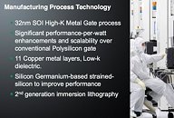
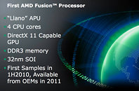
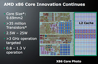
AMD, in its presentation at the International Solid State Circuits Conference (ISSCC) 2010, presented its plan to build its much talked about 'Fusion' processor platform, codenamed Llano, central to which, is the Accelerated Processing Unit (APU). AMD's APU is expected to be the first design to embed a multi-core x86 CPU and a GPU onto a single die. This design goes a notch ahead of Intel's recently released 'Clarkdale' processor, where Intel strapped a 32 nm dual-core CPU die and a 45 nm northbridge die with integrated graphics, onto an MCM (multi chip module) package. Llano is also expected to feature four processing cores, along with other design innovations.

Some of the most notable announcements in AMD's presentation is that the company will begin sampling the chip to its industry partners within the first half of 2010. The Llano die will be build on a 32 nm High-K Metal Gate process. On this process, each x86 core will be as small as 9.69 mm². Other important components on the Llano die are a DDR3 memory controller, on-die northbridge, and a DirectX 11 compliant graphics core derived from the Evergreen family of GPUs. The x86 cores are expected to run at speeds of over 3 GHz. Each core has 1 MB of dedicated L2 cache, taking the total chip cache size to 4 MB.
Return to Keyword Browsing
Nov 21st, 2024 10:14 EST change timezone

New Forum Posts

Popular Reviews

Controversial News Posts