Numem to Showcase Next-Gen Memory Solutions at the Upcoming Chiplet Summit
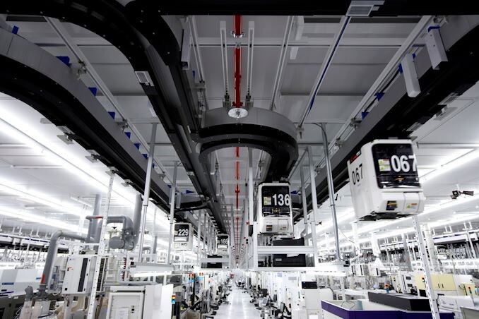
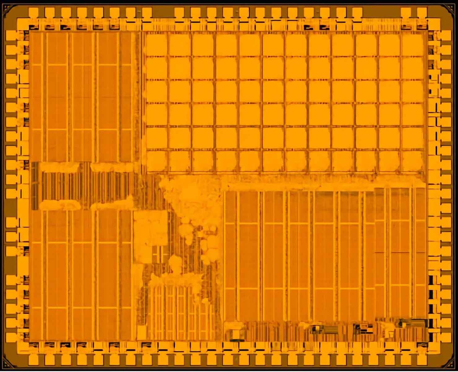
Numem, an innovator focused on accelerating memory for AI workloads, will be at the upcoming Chiplet Summit to showcase its high-performance solutions. By accelerating the delivery of data via new memory subsystem designs, Numem solutions are re-architecting the hierarchy of AI memory tiers to eliminate the bottlenecks that negatively impact power and performance.
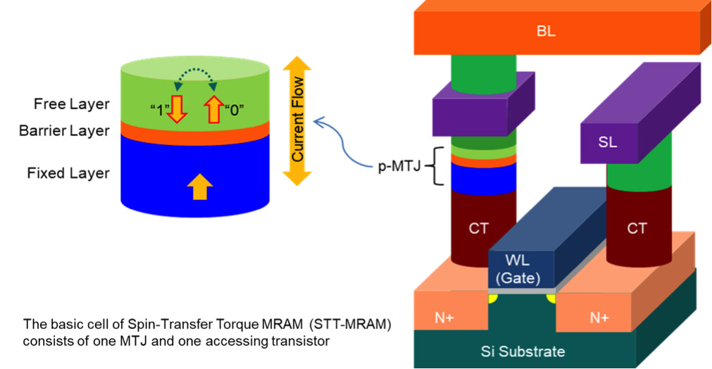
The rapid growth of AI workloads and AI Processor/GPUs are exacerbating the memory bottleneck caused by the slowing performance improvements and scalability of SRAM and DRAM - presenting a major obstacle to maximizing system performance. To overcome this, there is a pressing need for intelligent memory solutions that offer higher power efficiency and greater bandwidth, coupled with a reevaluation of traditional memory architectures.
The rapid growth of AI workloads and AI Processor/GPUs are exacerbating the memory bottleneck caused by the slowing performance improvements and scalability of SRAM and DRAM - presenting a major obstacle to maximizing system performance. To overcome this, there is a pressing need for intelligent memory solutions that offer higher power efficiency and greater bandwidth, coupled with a reevaluation of traditional memory architectures.