Apr 16th, 2025 09:19 EDT
change timezone
Latest GPU Drivers
New Forum Posts
- Last game you purchased? (772)
- Help me identify Chip of this DDR4 RAM (20)
- 5070ti overclock...what are your settings? (5)
- Windows 11 fresh install to do list (23)
- How to relubricate a fan and/or service a troublesome/noisy fan. (229)
- GPU Memory Temprature is always high (16)
- Help For XFX RX 590 GME Chinese - Vbios (4)
- PCGH: "hidden site" to see total money spend on steam (3)
- Share your AIDA 64 cache and memory benchmark here (3053)
- NVFlash for RTX 50 Series (Blackwell) (0)
Popular Reviews
- G.SKILL Trident Z5 NEO RGB DDR5-6000 32 GB CL26 Review - AMD EXPO
- ASUS GeForce RTX 5080 TUF OC Review
- DAREU A950 Wing Review
- The Last Of Us Part 2 Performance Benchmark Review - 30 GPUs Compared
- Sapphire Radeon RX 9070 XT Pulse Review
- Sapphire Radeon RX 9070 XT Nitro+ Review - Beating NVIDIA
- Upcoming Hardware Launches 2025 (Updated Apr 2025)
- Thermaltake TR100 Review
- Zotac GeForce RTX 5070 Ti Amp Extreme Review
- TerraMaster F8 SSD Plus Review - Compact and quiet
Controversial News Posts
- NVIDIA GeForce RTX 5060 Ti 16 GB SKU Likely Launching at $499, According to Supply Chain Leak (182)
- NVIDIA Sends MSRP Numbers to Partners: GeForce RTX 5060 Ti 8 GB at $379, RTX 5060 Ti 16 GB at $429 (124)
- Nintendo Confirms That Switch 2 Joy-Cons Will Not Utilize Hall Effect Stick Technology (105)
- Over 200,000 Sold Radeon RX 9070 and RX 9070 XT GPUs? AMD Says No Number was Given (100)
- Nintendo Switch 2 Launches June 5 at $449.99 with New Hardware and Games (99)
- Sony Increases the PS5 Pricing in EMEA and ANZ by Around 25 Percent (85)
- NVIDIA PhysX and Flow Made Fully Open-Source (77)
- NVIDIA Pushes GeForce RTX 5060 Ti Launch to Mid-April, RTX 5060 to May (77)
News Posts matching #NAND
Return to Keyword Browsing"DRAM+" Non-Volatile Memory Combines DRAM Speed With Flash Persistence
Ferroelectric Memory Co. (FMC) and Neumonda have formed a partnership to commercialize "DRAM+," a ferroelectric (FeRAM) memory architecture combining DRAM's speed with non-volatile data retention. The technology substitutes conventional capacitors with ferroelectric hafnium oxide (HfO₂) elements, allowing persistent storage without power while maintaining nanosecond access times. This hybrid technology addresses the performance gap between high-speed DRAM and storage-class memory like NAND flash. Unlike previous European DRAM ventures from Infineon and Qimonda that failed against commodity memory economics, FMC targets specialized applications valuing persistence and power efficiency. The HfO₂-based approach resolves limitations of previous FeRAM memory implementations using lead zirconate titanate (PZT) that couldn't scale beyond megabyte capacities.
Prototypes now demonstrate gigabit-range densities compatible with sub-10 nm fabrication of traditional DRAM made by Micron, Samsung, SK Hynix, and others. By eliminating refresh cycles, DRAM+ reduces static power consumption substantially compared to traditional one-transistor/one-capacitor DRAM cells. Primary applications include AI accelerators requiring persistent model weights, automotive ECUs with immediate startup requirements, and power-constrained medical implants. Neumonda will contribute its test platform suite Rhinoe, Octopus, and Raptor for electrical characterization and analytics at lower capital costs than standard semiconductor test equipment. No production timeline has been announced for commercial DRAM+ products.
Prototypes now demonstrate gigabit-range densities compatible with sub-10 nm fabrication of traditional DRAM made by Micron, Samsung, SK Hynix, and others. By eliminating refresh cycles, DRAM+ reduces static power consumption substantially compared to traditional one-transistor/one-capacitor DRAM cells. Primary applications include AI accelerators requiring persistent model weights, automotive ECUs with immediate startup requirements, and power-constrained medical implants. Neumonda will contribute its test platform suite Rhinoe, Octopus, and Raptor for electrical characterization and analytics at lower capital costs than standard semiconductor test equipment. No production timeline has been announced for commercial DRAM+ products.


Report Suggests that Samsung Will Increase DRAM & NAND Prices by 3 to 5%
Earlier today, industry moles in South Korea have heard whispers about Samsung Electronics planning a new pricing strategy for NAND and DRAM product lines. According to an MK news articles, local sources believe that company leadership will: "raise memory chip prices—by 3-5% from the current level—for major global customers. It is reported that some customers have already begun contract negotiations that reflect the increase conditions." Regional watchdogs posit that the megacorporation is reacting to very current geopolitical tensions (i.e. tariffs). Earlier this week, a main rival—Micron—informed customers about forthcoming memory price increases. Naturally, the North American memory chip giant is not "fully" affected by recent seismic shifts. A "significant growth demand" has caused jacked up charges—effective across DRAM, NAND flash, and HBM portfolios—projected throughout 2025 and 2026.
Returning to South Korean shores and Samsung, one unnamed semiconductor insider opined to MK: "oversupply continued throughout last year, but supply has recently decreased as major companies have begun to reduce production...In addition, artificial intelligence (AI) devices are appearing one after another in China, and demand for semiconductors is gradually increasing due to industrial automation." DRAMeXchange—an appropriately named market research organization—has kept track relevant trends. As disclosed by the MK news piece—as of last month, general-purpose DRAM DDR4 prices: "remained flat for the fourth month in a row." Looking at conditions for DDR5 (used in high-performance PCs and enterprise equipment), prices soared by 12%. DRAMeXchange observed NAND costs rising by 9.6%: "continuing an upward trend for the third consecutive month."


Returning to South Korean shores and Samsung, one unnamed semiconductor insider opined to MK: "oversupply continued throughout last year, but supply has recently decreased as major companies have begun to reduce production...In addition, artificial intelligence (AI) devices are appearing one after another in China, and demand for semiconductors is gradually increasing due to industrial automation." DRAMeXchange—an appropriately named market research organization—has kept track relevant trends. As disclosed by the MK news piece—as of last month, general-purpose DRAM DDR4 prices: "remained flat for the fourth month in a row." Looking at conditions for DDR5 (used in high-performance PCs and enterprise equipment), prices soared by 12%. DRAMeXchange observed NAND costs rising by 9.6%: "continuing an upward trend for the third consecutive month."


Micron Announces Memory Price Increases for 2025-2026 Amid Supply Constraints
In a letter to customers, Micron has announced upcoming memory price increases extending through 2025 and 2026, citing persistent supply constraints coupled with accelerating demand across its product portfolio. The manufacturer points to significant demand growth in DRAM, NAND flash, and high-bandwidth memory (HBM) segments as key drivers behind the pricing strategy. The memory market is rebounding from a prolonged oversupply cycle that previously depressed revenues industry-wide. Strategic production capacity reductions implemented by major suppliers have contributed to price stabilization and subsequent increases over the past twelve months. This pricing trajectory is expected to continue as data center operators, AI deployments, and consumer electronics manufacturers compete for limited memory allocation.
In communications to channel partners, Micron emphasized AI and HPC requirements as critical factors necessitating the price adjustments. The company has requested detailed forecast submissions from partners to optimize production planning and supply chain stability during the constrained market period. With its pricing announcement, Micron disclosed a $7 billion investment in a Singapore-based HBM assembly facility. The plant will begin operations in 2026 and will focus on HBM3E, HBM4, and HBM4E production—advanced memory technologies essential for next-generation AI accelerators and high-performance computing applications from NVIDIA, AMD, Intel, and other companies. The price increases could have cascading effects across the AI and GPU sector, potentially raising costs for products ranging from consumer gaming systems to enterprise data infrastructure. We are monitoring how these adjustments will impact hardware refresh cycles and technology adoption rates as manufacturers pass incremental costs to end customers.
In communications to channel partners, Micron emphasized AI and HPC requirements as critical factors necessitating the price adjustments. The company has requested detailed forecast submissions from partners to optimize production planning and supply chain stability during the constrained market period. With its pricing announcement, Micron disclosed a $7 billion investment in a Singapore-based HBM assembly facility. The plant will begin operations in 2026 and will focus on HBM3E, HBM4, and HBM4E production—advanced memory technologies essential for next-generation AI accelerators and high-performance computing applications from NVIDIA, AMD, Intel, and other companies. The price increases could have cascading effects across the AI and GPU sector, potentially raising costs for products ranging from consumer gaming systems to enterprise data infrastructure. We are monitoring how these adjustments will impact hardware refresh cycles and technology adoption rates as manufacturers pass incremental costs to end customers.


Intel to Receive $1.9 Billion as SK Hynix Finalizes NAND Deal
Intel and SK Hynix have finalized an $8.85 billion transaction involving Intel's NAND flash memory operations, marking the conclusion of a two-phase deal initiated in 2020. In the first phase of the transaction, SK Hynix acquired Intel's SSD division along with a NAND production facility in Dalian, China, for $6.61 billion. The Dalian facility was later rebranded as Solidigm. Notably, this phase transferred only the physical assets and operational facilities, leaving behind critical intellectual property, research and development infrastructure, and specialized technical staff. The second phase, finalized with a payment of $1.9 billion this Tuesday, addressed these remaining components. With this payment, SK Hynix secured full rights to Intel's proprietary NAND technology, R&D resources, and the technical workforce dedicated to NAND operations.
During the transition period, Intel maintained control over these elements, which limited integration between Solidigm and Intel's NAND teams. This separation was designed to manage operational risks and gradually transfer capabilities. Completing this deal helps with a strategic restructuring of Intel's portfolio as it shifts focus toward high-growth areas such as AI chip development, foundry services, and next-generation semiconductor manufacturing. A $1.9 billion financial injection is perfect in time for Intel Foundry business, burning billions per year, to offset some of the losses. For SK Hynix, consolidating the complete range of Intel's NAND operations enhances its competitive position in the global NAND market, providing access to established technologies and key industry expertise. This finalization is part of a broader trend where companies divest from commoditized memory products to concentrate on more advanced semiconductor solutions like AI chips and other accelerators, which are enjoying higher margins and a better business outlook.
During the transition period, Intel maintained control over these elements, which limited integration between Solidigm and Intel's NAND teams. This separation was designed to manage operational risks and gradually transfer capabilities. Completing this deal helps with a strategic restructuring of Intel's portfolio as it shifts focus toward high-growth areas such as AI chip development, foundry services, and next-generation semiconductor manufacturing. A $1.9 billion financial injection is perfect in time for Intel Foundry business, burning billions per year, to offset some of the losses. For SK Hynix, consolidating the complete range of Intel's NAND operations enhances its competitive position in the global NAND market, providing access to established technologies and key industry expertise. This finalization is part of a broader trend where companies divest from commoditized memory products to concentrate on more advanced semiconductor solutions like AI chips and other accelerators, which are enjoying higher margins and a better business outlook.

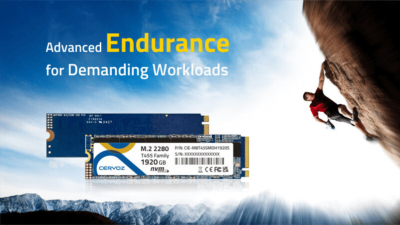
Cervoz Announces T455 NVMe SSD Series - Offering Advanced Endurance for Demanding Industries
In industrial environments, equipment runs 24/7, handling frequent and intensive write operations. To support these demanding workloads, storage solutions must offer high endurance to extend lifespan, minimize downtime, and lower Total Cost of Ownership (TCO). Designed to meet these demands, the Cervoz T455 Series, M.2 2280 NVMe SSD delivers 35% greater endurance through a refined firmware architecture and proven storage technologies. Ideal for industrial automation, edge computing, and high-performance computing (HPC), it ensures reliable performance under heavy workloads.
Enhanced Endurance for Demanding Industrial Applications—Over-Provisioning Technology: Endurance SSD Performance and Longevity
Cervoz's Over-Provisioning technology optimizes SSD performance by reserving extra storage space, boosting efficiency, and extending lifespan. How SSD Over-Provisioning Delivers Benefits:
- Extended Lifespan: Efficiently reserves additional storage space, enhancing NAND durability at least 35%.
- Consistent Performance: Maintains steady performance levels even under high-intensity workloads.
- Optimized Resource Management: Reserved space allocation for optimal write efficiency.
NAND Flash Prices Begin to Recover in 2Q25 as Production Cuts and Inventory Rebuilding Take Effect
TrendForce reports that NAND Flash suppliers began reducing production in the fourth quarter of 2024, and the effects are now starting to show. In anticipation of potential U.S. tariff increases, consumer electronics brands have accelerated production, further driving up demand. Concurrently, inventory restocking is underway across the PC, smartphone, and data center sectors. As a result, NAND Flash prices are expected to stabilize in the second quarter of 2025, with prices for wafers and client SSDs projected to rise.
Client SSD prices to rise 3-8% while enterprise SSD prices to remain flat
After three consecutive quarters of inventory depletion, client SSD demand is rebounding as OEMs resume production early. The upcoming end of Windows 10 support and the launch of new-generation CPUs are expected to drive replacement demand for PCs. Meanwhile, the DeepSeek effect is accelerating the adoption of edge AI, further fueling client SSD demand. With production cuts and supply adjustments gradually restoring balance, client SSD contract prices are projected to rise 3% to 8% QoQ in Q2.

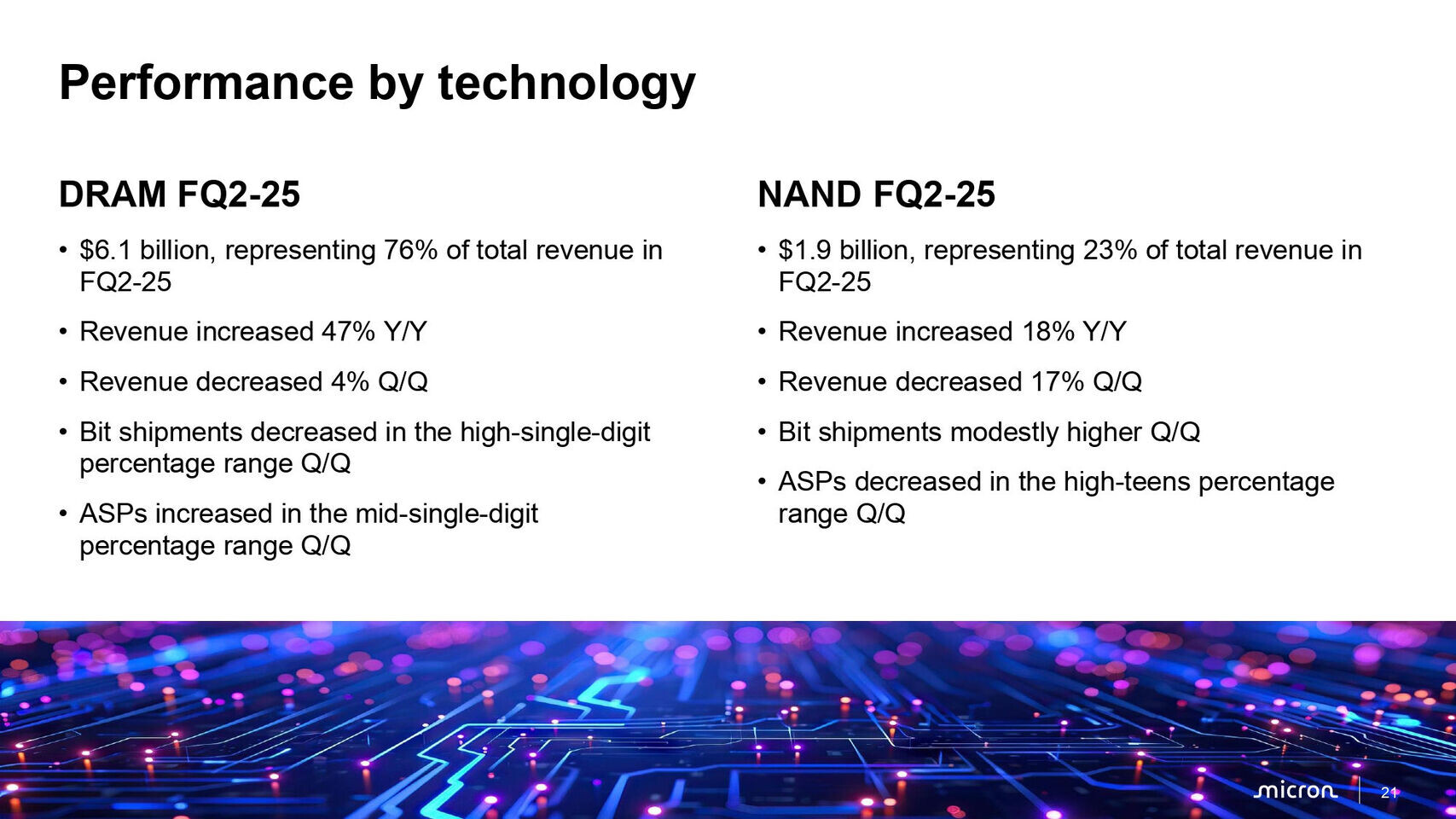
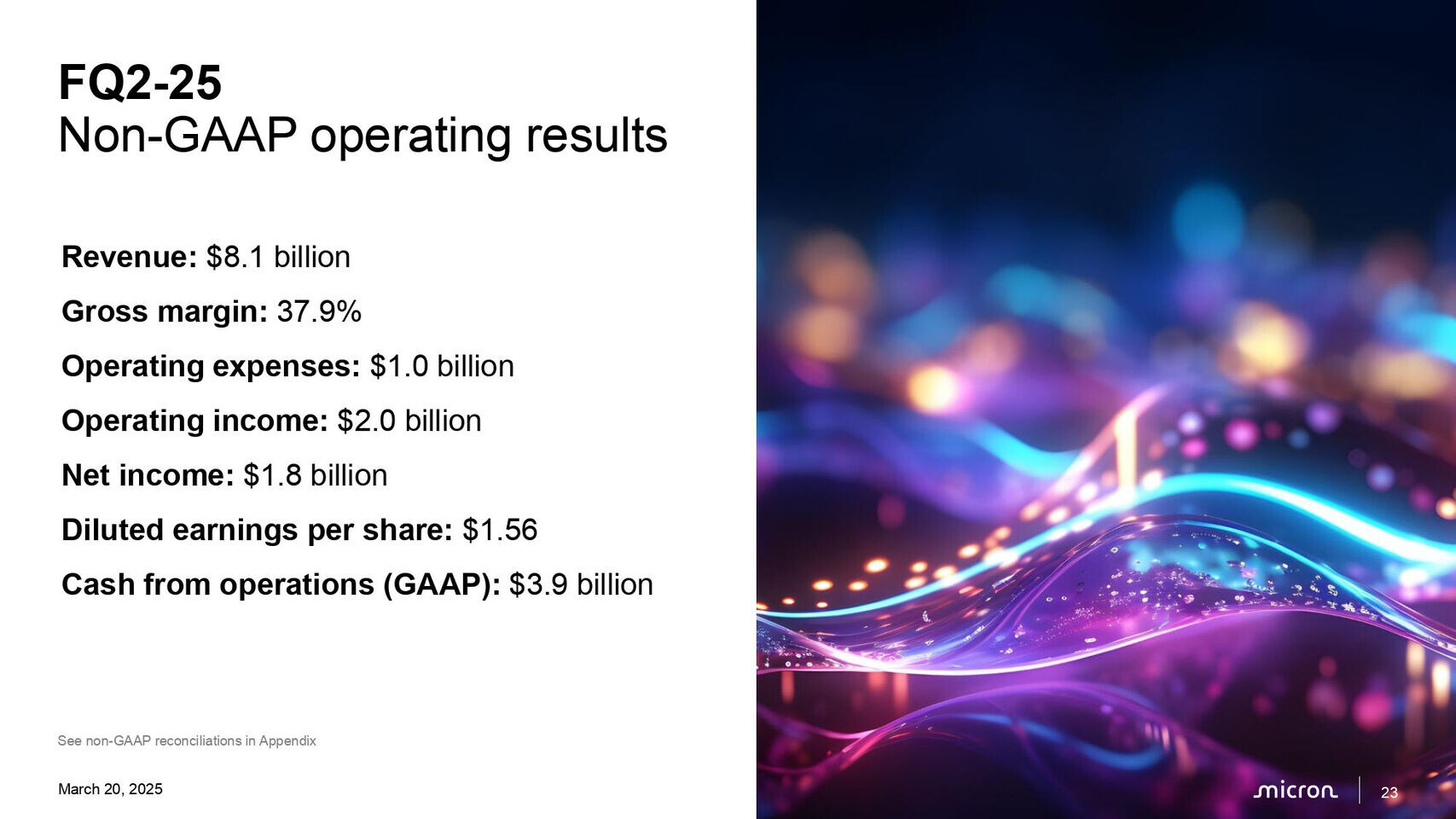
Micron Technology Reports Results for the Second Quarter of Fiscal 2025
Micron Technology, Inc. (Nasdaq: MU) today announced results for its second quarter of fiscal 2025, which ended February 27, 2025.
Fiscal Q2 2025 highlights


Fiscal Q2 2025 highlights
- Revenue of $8.05 billion versus $8.71 billion for the prior quarter and $5.82 billion for the same period last year
- GAAP net income of $1.58 billion, or $1.41 per diluted share
- Non-GAAP net income of $1.78 billion, or $1.56 per diluted share
- Operating cash flow of $3.94 billion versus $3.24 billion for the prior quarter and $1.22 billion for the same period last year


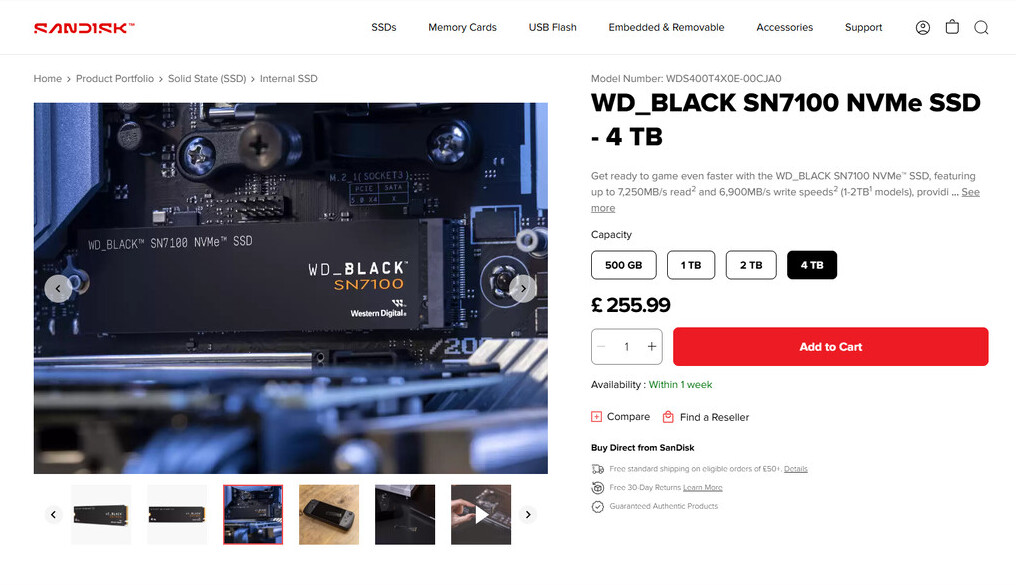
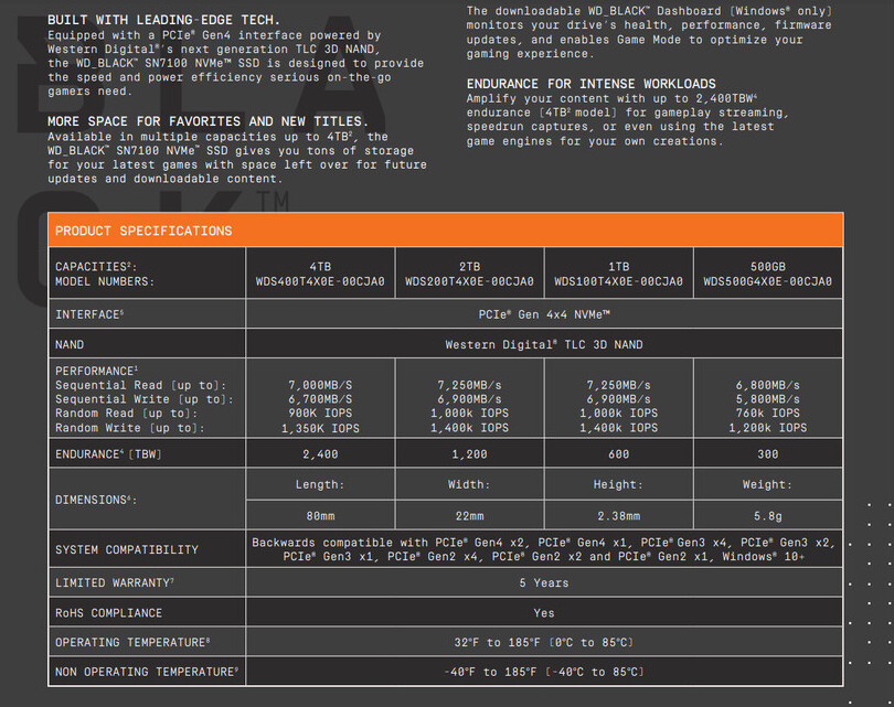
Western Digital Black SN7100 4 TB Variant Due for Imminent Release
Last November, Western Digital introduced its WD_BLACK SN7100 NVMe SSD series—advertised as utilizing their: "latest TLC 3D NAND." This new SSD design offers: "speeds up to 7,250 MB/s read and 6,900 MB/s write (for 1 and 2 TB models), providing up to a 35% performance boost over our previous generation SSD." The manufacturer's official press material did not explicitly state that the SN7100 would serve as a natural replacement for their well-regarded SN770 (2022) product family, but W1zzard's recent glowing review (of the 2 TB variant) refers back to the forebear on multiple occasions.
As low-key teased by last November's press announcement, a 4 TB WD_BLACK SN7100 model is arriving in 2025—freshly updated listings indicate an imminent launch at retail/e-tail. Interestingly, WD's SN770 range never reached beyond a 2 TB barrier. Search engine results—when inputting the "WDS400T4X0E-00CJA0" identifier—point to a "March 2025" SN7100 series data sheet, and SanDisk's UK store accepting pre-orders for £255.99 (~$332 USD). Availability status is currently designated as: "within 1 week." Western Digital's spec comparison table (see below) proudly showcases the 4 TB variant's impressive endurance (TBW) credential: 2400. Its lower capacity siblings (1 TB and 2 TB) hold slight advantages in terms of read and write speeds. TechPowerUp's resident SSD reviewer deemed the SN7100 2 TB model worthy of an "Editor's Choice" badge, but wished for a larger capacity option. We hope that a 4 TB evaluation sample will make its way to W1zz HQ in the near future.


As low-key teased by last November's press announcement, a 4 TB WD_BLACK SN7100 model is arriving in 2025—freshly updated listings indicate an imminent launch at retail/e-tail. Interestingly, WD's SN770 range never reached beyond a 2 TB barrier. Search engine results—when inputting the "WDS400T4X0E-00CJA0" identifier—point to a "March 2025" SN7100 series data sheet, and SanDisk's UK store accepting pre-orders for £255.99 (~$332 USD). Availability status is currently designated as: "within 1 week." Western Digital's spec comparison table (see below) proudly showcases the 4 TB variant's impressive endurance (TBW) credential: 2400. Its lower capacity siblings (1 TB and 2 TB) hold slight advantages in terms of read and write speeds. TechPowerUp's resident SSD reviewer deemed the SN7100 2 TB model worthy of an "Editor's Choice" badge, but wished for a larger capacity option. We hope that a 4 TB evaluation sample will make its way to W1zz HQ in the near future.

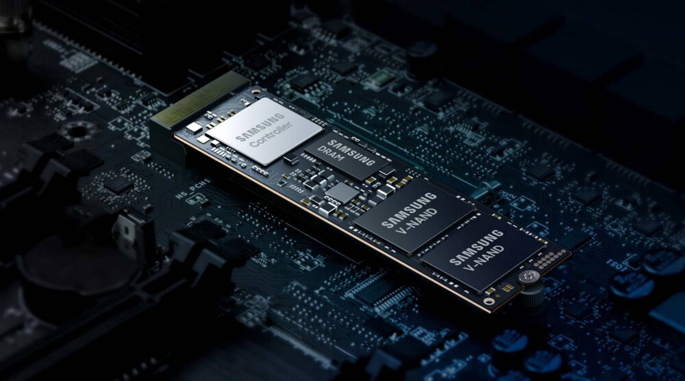
Samsung 9100 PRO Series SSD with up to 14.8 GB/s Read Speed is Now Available
Samsung has officially released its next-generation 9100 PRO series solid-state drives to the masses, with availability starting today. The drives leverage PCIe 5.0 technology to deliver sequential read/write speeds of up to 14,800/13,400 MB/s—twice as fast as previous generation offerings—while random read/write performance reaches 2,200K/2,600K IOPS. The series, available in standard and heatsink variants, marks Samsung's first consumer NVMe offerings to reach 8 TB capacity. The 9100 PRO line integrates Samsung's 5 nm controller architecture, yielding up to 49% improved power efficiency compared to prior models. This efficiency gain comes without compromising the form factor, with the drives maintaining a slim 0.35-inch profile. The heatsink variant provides additional thermal regulation capabilities for sustained performance under demanding workloads, making it particularly suitable for AI content generation, 8K video editing, and high-performance gaming applications.
Currently available configurations include 1 TB, 2 TB, and 4 TB capacities, with pricing starting at $199.99 for the standard 1 TB model and $219.99 for the heatsink-equipped equivalent. The 2 TB models are priced at $299.99 and $319.99, respectively, while 4 TB variants command $549.99 and $569.99. Samsung has announced that 8 TB models will enter the market in H2 2025. Compatible with desktop PCs, laptops, and PlayStation 5 consoles featuring appropriate PCIe 5.0 slots, the drives incorporate Samsung's V-NAND TLC (V8) technology and LPDDR4X cache memory—ranging from 1 GB in the 1 TB model to 8 GB in the 8 TB version. Samsung's Magician Software suite provides management capabilities, including performance optimization and firmware update notifications.


Currently available configurations include 1 TB, 2 TB, and 4 TB capacities, with pricing starting at $199.99 for the standard 1 TB model and $219.99 for the heatsink-equipped equivalent. The 2 TB models are priced at $299.99 and $319.99, respectively, while 4 TB variants command $549.99 and $569.99. Samsung has announced that 8 TB models will enter the market in H2 2025. Compatible with desktop PCs, laptops, and PlayStation 5 consoles featuring appropriate PCIe 5.0 slots, the drives incorporate Samsung's V-NAND TLC (V8) technology and LPDDR4X cache memory—ranging from 1 GB in the 1 TB model to 8 GB in the 8 TB version. Samsung's Magician Software suite provides management capabilities, including performance optimization and firmware update notifications.


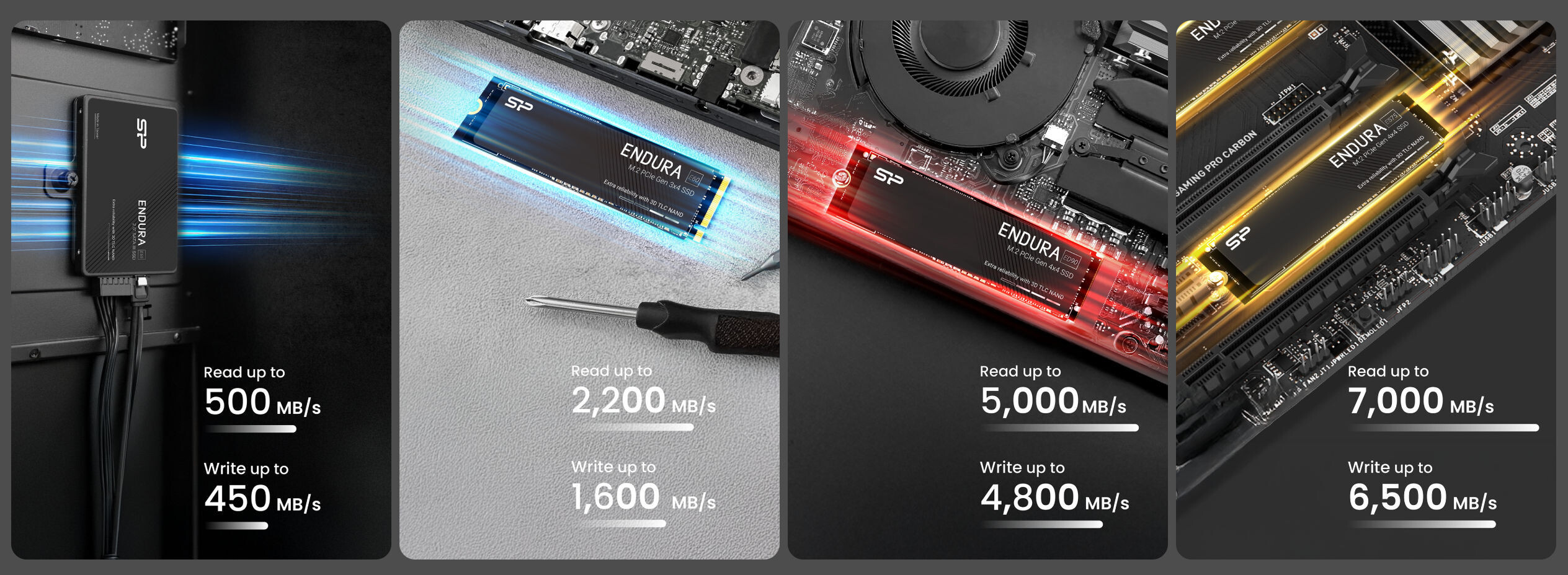
Silicon Power Launches Four Advanced TLC SSDs Under the New Endura Series
Silicon Power (SP) is excited to launch the Endura series, a new SSD lineup featuring four models: E55, E60, ED90, and ES75. Designed with advanced 3D TLC NAND technology, these SSDs offer a comprehensive range of storage solutions catering to diverse user needs, all with the reliability- and performance-geared features that define TLC.
E55: 2.5" SATA III SSD
The E55 delivers robust and stable performance, making it an ideal choice for casual users and system integration builders seeking accessible, dependable storage. With a SATA III 6 Gb/s interface and capacities ranging from 512 GB to 2 TB, it offers broad compatibility for diverse devices and storage needs. Delivering speeds up to 500 MB/s read and 450 MB/s write - 15 times faster than a standard HDD - the E55 combines reliability and familiarity in a versatile, user-friendly solution.


Phison Showcases Edge AI and Embedded Solutions at Embedded World
Embedded World is one of the most influential exhibitions in the global embedded technology sector, attracting numerous experts in industrial computing, automotive electronics, IoT, and AI technologies each year. Phison Electronics (8299TT), a leading innovator of NAND controller and NAND storage solutions, will participate in the Taiwan Excellence Pavilion at Embedded World 2025 in Germany from March 11 to 13.
Phison will showcase its exclusive AI solution aiDAPTIV+, the enterprise ultra-high-capacity PASCARI PCIe 5.0 122.88 TB SSD, and its latest automotive storage technology, the MPT5 Automotive PCIe Gen 4 SSD, demonstrating over 15 years of technical expertise in the embedded market.
Phison will showcase its exclusive AI solution aiDAPTIV+, the enterprise ultra-high-capacity PASCARI PCIe 5.0 122.88 TB SSD, and its latest automotive storage technology, the MPT5 Automotive PCIe Gen 4 SSD, demonstrating over 15 years of technical expertise in the embedded market.

Silicon Motion Showcases Storage Solutions for AI and Display Interface SoCs at Embedded World 2025
Silicon Motion Technology Corporation, a global leader in NAND flash controllers for solid-state storage devices, today announced its participation in Embedded World 2025, taking place from March 11-13, 2025, in Nuremberg, Germany.
At the event, Silicon Motion will showcase its latest storage and display interface solutions, including PCIe NVMe Gen 4/5 SSD controllers, Ferri embedded storage solutions, and advanced display interface SoCs. These cutting-edge innovations are designed to maximize performance per watt, extend device longevity and power for the next generation of AI-driven industrial, embedded, automotive, and data center applications.


At the event, Silicon Motion will showcase its latest storage and display interface solutions, including PCIe NVMe Gen 4/5 SSD controllers, Ferri embedded storage solutions, and advanced display interface SoCs. These cutting-edge innovations are designed to maximize performance per watt, extend device longevity and power for the next generation of AI-driven industrial, embedded, automotive, and data center applications.


Weak Consumer Electronics Demand Drives 4Q24 NAND Flash Revenue Down 6.2% QoQ, Says TrendForce
TrendForce's latest research reveals that the NAND Flash market faced downward pressure in 4Q24 as PC and smartphone manufacturers continued inventory clearance efforts, leading to significant supply chain adjustments. Consequently, NAND Flash prices reversed downward, with ASP dropping 4% QoQ, while overall bit shipments declined by 2%. Total industry revenue fell 6.2% QoQ to US$16.52 billion.
Looking ahead to 1Q25, the traditional slow season effect remains unavoidable despite suppliers actively reducing production. Server and other key end-market inventory restocking has slowed, and with both order volumes and contract prices declining sharply. NAND Flash industry revenue is expected to drop by up to 20% QoQ. However, as production cuts take effect and prices stabilize, the NAND Flash market is expected to recover in the second half of 2025.
Looking ahead to 1Q25, the traditional slow season effect remains unavoidable despite suppliers actively reducing production. Server and other key end-market inventory restocking has slowed, and with both order volumes and contract prices declining sharply. NAND Flash industry revenue is expected to drop by up to 20% QoQ. However, as production cuts take effect and prices stabilize, the NAND Flash market is expected to recover in the second half of 2025.

Samsung Aims for 1,000-Layer NAND by 2030, Begins Wafer Bonding at 400 Layers
Samsung aims to create 1,000-layer NAND by 2030 relying on its new "multi-BV" NAND design. The Bell reports that this plan involves stacking four wafers to overcome structural limits. Wafer bonding technology plays a crucial role in this progress and Samsung intends to use it to break the 1,000-layer barrier. Samsung Electronics DS division CTO, Song Jae-hyuk, pointed out that wafer bonding allows separate production of peripheral and cell wafers before joining them into one semiconductor. The Bell says this technology will likely appear first in Samsung's 10th-gen NAND (V10), while industry experts think a single wafer can hold about 500 NAND layers when implementing only cell structures. In the past, Samsung has used the COP (Cell on Peripheral) technique, a method that places the peripheral circuit on one wafer, with NAND cells stacked on top. However, as NAND layers grow, the lower peripheral parts face more pressure potentially affecting reliability.
Samsung's plan involves working with China's YMTC, which should offer a hybrid bonding patent for V10 NAND. ZDNet reports that the South Korean tech company will start making its V10 NAND in large quantities in the second half of 2025, with about 420-430 layers. Besides wafer bonding, Samsung adds other technologies to its NAND plan. The Bell points out that cold etching using molybdenum, and other new ideas will start with 400-layer NAND and play a key part in growing to 1,000 layers. Samsung isn't alone in trying to create ultra-high-layer NAND products. Japan's Kioxia also wants to reach this goal through its "multi-stack CBA" (CMOS Bonded to Array) technology. The company's plan is even bolder hoping to sell 1,000-layer 3D NAND by 2027.
Samsung's plan involves working with China's YMTC, which should offer a hybrid bonding patent for V10 NAND. ZDNet reports that the South Korean tech company will start making its V10 NAND in large quantities in the second half of 2025, with about 420-430 layers. Besides wafer bonding, Samsung adds other technologies to its NAND plan. The Bell points out that cold etching using molybdenum, and other new ideas will start with 400-layer NAND and play a key part in growing to 1,000 layers. Samsung isn't alone in trying to create ultra-high-layer NAND products. Japan's Kioxia also wants to reach this goal through its "multi-stack CBA" (CMOS Bonded to Array) technology. The company's plan is even bolder hoping to sell 1,000-layer 3D NAND by 2027.
Numemory Releases Optane Successor: "NM101" Storage-Class Memory
Numemory has introduced the NM101, a 64 Gb storage-class memory module that uses technology similar to Intel's now-discontinued Optane architecture. The device implements phase-change memory and crossbar technology in a 3D selector-only memory structure, matching Optane's 3200 MT/s transfer rate specification. The technical architecture diverges from Intel's implementation by using a single selector in its cross-point structure rather than the dual-selector approach of 3D XPoint memory. Operating at 1.2 V with an X8 bus width, the NM101 uses 3D stacking to achieve claimed performance metrics of 10x faster read/write speeds than NAND flash. Xincun Technology, which established the Numemory division in Wuhan in 2022, holds 273 patents related to the technology, including 60 international and 213 Chinese patents. The company's R&D team of 144 engineers has developed the architecture since 2019, three years before Intel ended its Optane program.
Production plans specify an initial manufacturing target of 10,000 units monthly by the end of 2025. Guao Technology has committed ¥10 billion to establish production facilities in Zhejiang province, with additional funding from the Anji county government. The NM101's operating temperature range spans 0-70°C, suitable for standard data center environments. While the device's specifications suggest the potential for data center deployment, specific IOPS and latency metrics remain unpublished. Initial production will serve domestic Chinese servers and storage manufacturers. The technology's viability in mass production remains to be demonstrated, particularly given the manufacturing challenges that contributed to Optane's market exit. The Chinese internal market is massive, so serving only domestic companies could be enough for Numemory at the beginning. If the company continues development, worldwide expansion could pick up where Optane stopped.

Production plans specify an initial manufacturing target of 10,000 units monthly by the end of 2025. Guao Technology has committed ¥10 billion to establish production facilities in Zhejiang province, with additional funding from the Anji county government. The NM101's operating temperature range spans 0-70°C, suitable for standard data center environments. While the device's specifications suggest the potential for data center deployment, specific IOPS and latency metrics remain unpublished. Initial production will serve domestic Chinese servers and storage manufacturers. The technology's viability in mass production remains to be demonstrated, particularly given the manufacturing challenges that contributed to Optane's market exit. The Chinese internal market is massive, so serving only domestic companies could be enough for Numemory at the beginning. If the company continues development, worldwide expansion could pick up where Optane stopped.


Kioxia and Sandisk Unveil Next-Generation 3D Flash Memory Technology Achieving 4.8Gb/s NAND Interface Speed
Kioxia Corporation and Sandisk Corporation have pioneered a state-of-the-art 3D flash memory technology, setting the industry benchmark with a 4.8 Gb/s NAND interface speed, superior power efficiency, and heightened density
Unveiled at ISSCC 2025, the new 3D flash memory innovation, together with the companies' revolutionary CBA (CMOS directly Bonded to Array) technology, incorporates one of the latest interface standards, Toggle DDR6.0 for NAND flash memory, and leverages the SCA (Separate Command Address) protocol, a novel command address input method of its interface, and PI-LTT (Power Isolated Low-Tapped Termination) technology, which is instrumental in further reducing power consumption.
Unveiled at ISSCC 2025, the new 3D flash memory innovation, together with the companies' revolutionary CBA (CMOS directly Bonded to Array) technology, incorporates one of the latest interface standards, Toggle DDR6.0 for NAND flash memory, and leverages the SCA (Separate Command Address) protocol, a novel command address input method of its interface, and PI-LTT (Power Isolated Low-Tapped Termination) technology, which is instrumental in further reducing power consumption.

Micron Unveils Its First PCIe Gen5 NVMe High-Performance Client SSD
Micron Technology, Inc., today announced the Micron 4600 PCIe Gen 5 NVMe SSD, an innovative client storage drive for OEMs that is designed to deliver exceptional performance and user experience for gamers, creators and professionals. Leveraging Micron G9 TLC NAND, the 4600 SSD is Micron's first Gen 5 client SSD and doubles the performance of its predecessor.
The Micron 4600 SSD showcases sequential read speeds of 14.5 GB/s and write speeds of 12.0 GB/s. These capabilities allow users to load a large language model (LLM) from the SSD to DRAM in less than one second, enhancing the user experience with AI PCs. For AI model loading times, the 4600 SSD reduces load times by up to 62% compared to Gen 4 performance SSDs ensuring rapid deployment of LLMs and other AI workloads. Additionally, the 4600 SSD provides up to 107% improved energy efficiency (MB/s per watt) compared to Gen 4 performance SSDs, enhancing battery life and overall system efficiency.


The Micron 4600 SSD showcases sequential read speeds of 14.5 GB/s and write speeds of 12.0 GB/s. These capabilities allow users to load a large language model (LLM) from the SSD to DRAM in less than one second, enhancing the user experience with AI PCs. For AI model loading times, the 4600 SSD reduces load times by up to 62% compared to Gen 4 performance SSDs ensuring rapid deployment of LLMs and other AI workloads. Additionally, the 4600 SSD provides up to 107% improved energy efficiency (MB/s per watt) compared to Gen 4 performance SSDs, enhancing battery life and overall system efficiency.


Supplier Production Cuts and AI Demand Expected to Drive NAND Flash Price Recovery in 2H25
TrendForce's latest findings reveal that the NAND Flash market continues to be plagued by oversupply in the first quarter of 2025, leading to sustained price declines and financial strain for suppliers. However, TrendForce anticipates a significant improvement in the market's supply-demand balance in the second half of the year.
Key factors contributing to this shift include proactive production cuts by manufacturers, inventory reductions in the smartphone sector, and growing demand driven by AI and DeepSeek applications. These elements are expected to alleviate oversupply and support a price rebound for NAND Flash.
Key factors contributing to this shift include proactive production cuts by manufacturers, inventory reductions in the smartphone sector, and growing demand driven by AI and DeepSeek applications. These elements are expected to alleviate oversupply and support a price rebound for NAND Flash.

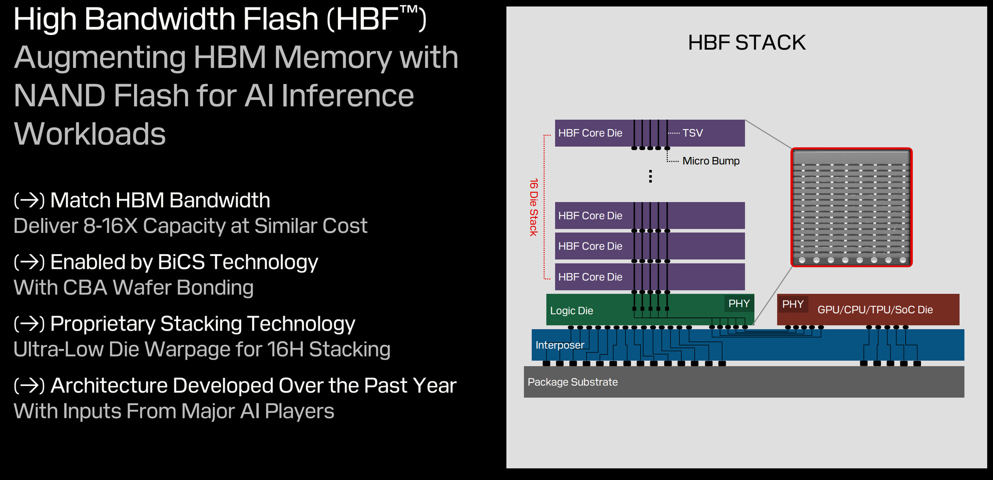
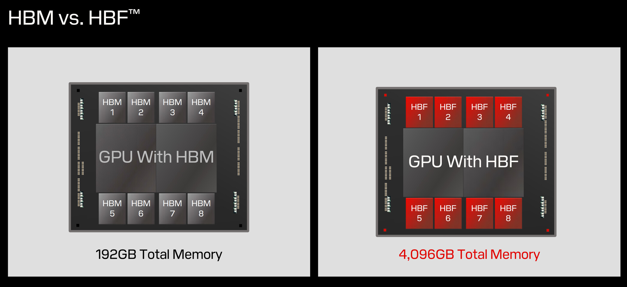
SanDisk Develops HBM Killer: High-Bandwidth Flash (HBF) Allows 4 TB of VRAM for AI GPUs
During its first post-Western Digital spinoff investor day, SanDisk showed something it has been working on to tackle the AI sector. High-bandwidth flash (HBF) is a new memory architecture that combines 3D NAND flash storage with bandwidth capabilities comparable to high-bandwidth memory (HBM). The HBF design stacks 16 3D NAND BiCS8 dies using through-silicon vias, with a logic layer enabling parallel access to memory sub-arrays. This configuration achieves 8 to 16 times greater capacity per stack than current HBM implementations. A system using eight HBF stacks can provide 4 TB of VRAM to store large AI models like GPT-4 directly on GPU hardware. The architecture breaks from conventional NAND design by implementing independently accessible memory sub-arrays, moving beyond traditional multi-plane approaches. While HBF surpasses HBM's capacity specifications, it maintains higher latency than DRAM, limiting its application to specific workloads.
SanDisk has not disclosed its solution for NAND's inherent write endurance limitations, though using pSLC NAND makes it possible to balance durability and cost. The bandwidth of HBF is also unknown, as the company hasn't put out details yet. SanDisk Memory Technology Chief Alper Ilkbahar confirmed the technology targets read-intensive AI inference tasks rather than latency-sensitive applications. The company is developing HBF as an open standard, incorporating mechanical and electrical interfaces similar to HBM to simplify integration. Some challenges remain, including NAND's block-level addressing limitations and writing endurance constraints. While these factors make HBF unsuitable for gaming applications, the technology's high capacity and throughput characteristics align with AI model storage and inference requirements. SanDisk has announced plans for three generations of HBF development, indicating a long-term commitment to the technology.


SanDisk has not disclosed its solution for NAND's inherent write endurance limitations, though using pSLC NAND makes it possible to balance durability and cost. The bandwidth of HBF is also unknown, as the company hasn't put out details yet. SanDisk Memory Technology Chief Alper Ilkbahar confirmed the technology targets read-intensive AI inference tasks rather than latency-sensitive applications. The company is developing HBF as an open standard, incorporating mechanical and electrical interfaces similar to HBM to simplify integration. Some challenges remain, including NAND's block-level addressing limitations and writing endurance constraints. While these factors make HBF unsuitable for gaming applications, the technology's high capacity and throughput characteristics align with AI model storage and inference requirements. SanDisk has announced plans for three generations of HBF development, indicating a long-term commitment to the technology.

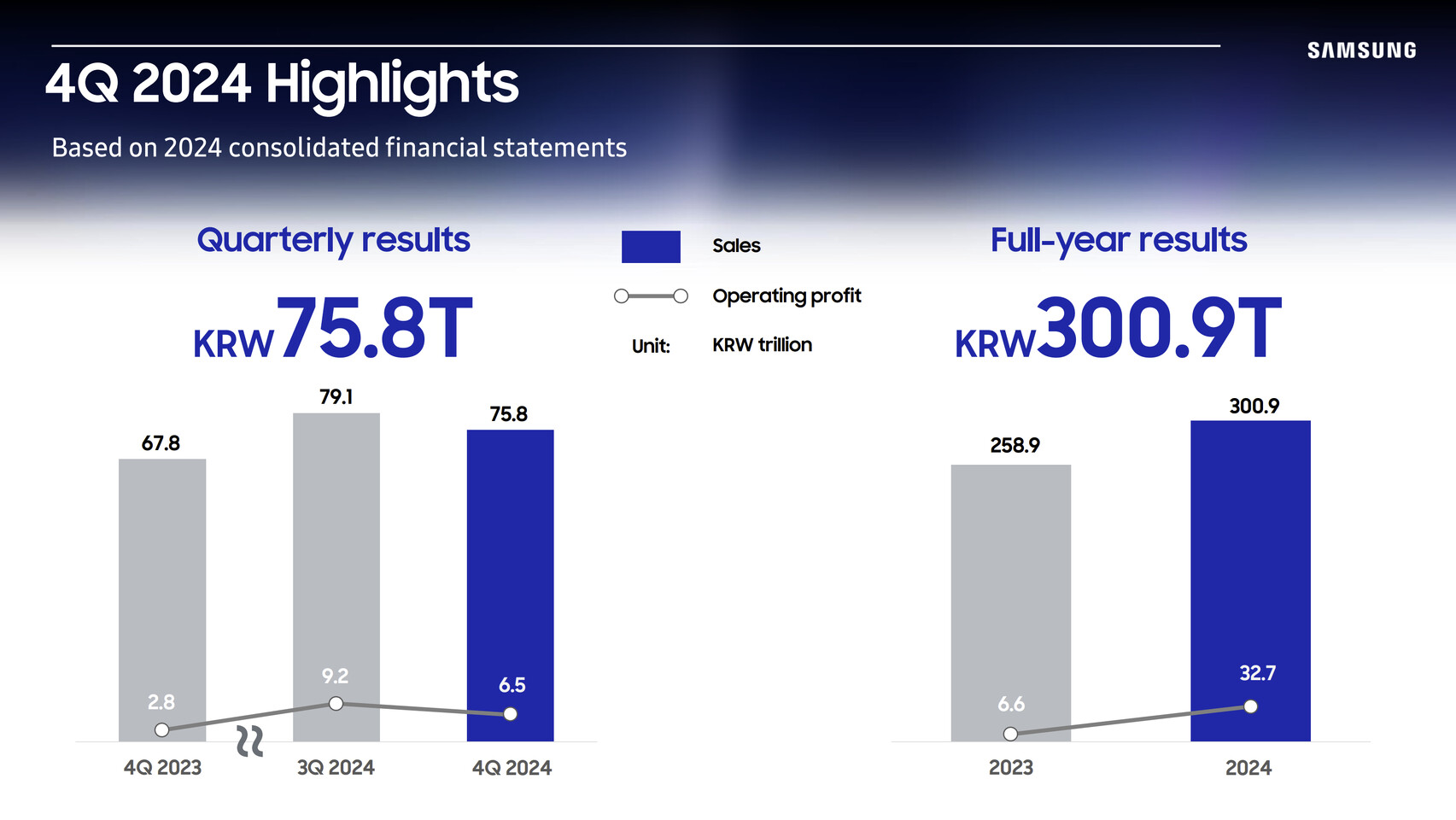
Samsung Electronics Announces Fourth Quarter and FY 2024 Results
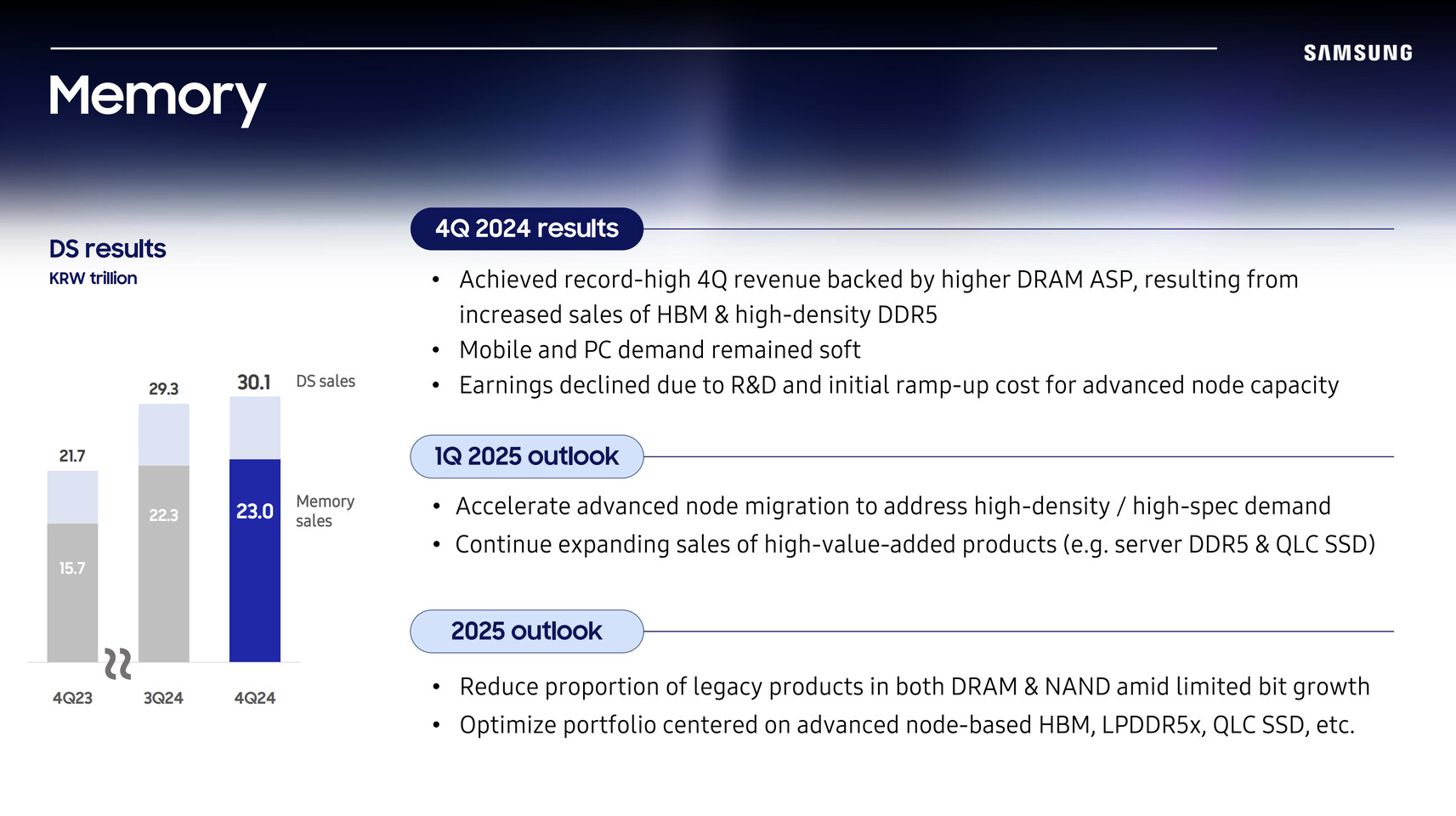
Samsung Electronics today reported financial results for the fourth quarter and the fiscal year 2024. The Company posted KRW 75.8 trillion in consolidated revenue and KRW 6.5 trillion in operating profit in the quarter ended December 31, 2024. For the full year, it reported KRW 300.9 trillion in annual revenue and KRW 32.7 trillion in operating profit.
Although fourth quarter revenue and operating profit decreased on a quarter-on-quarter (QoQ) basis, annual revenue reached the second-highest on record, surpassed only in 2022. Meanwhile, operating profit was down KRW 2.7 trillion QoQ, due to soft market conditions especially for IT products, and an increase in expenditures including R&D. In the first quarter of 2025, while overall earnings improvement may be limited due to weakness in the semiconductors business, the Company aims to pursue growth through increased sales of smartphones with differentiated AI experiences, as well as premium products in the Device eXperience (DX) Division.


Although fourth quarter revenue and operating profit decreased on a quarter-on-quarter (QoQ) basis, annual revenue reached the second-highest on record, surpassed only in 2022. Meanwhile, operating profit was down KRW 2.7 trillion QoQ, due to soft market conditions especially for IT products, and an increase in expenditures including R&D. In the first quarter of 2025, while overall earnings improvement may be limited due to weakness in the semiconductors business, the Company aims to pursue growth through increased sales of smartphones with differentiated AI experiences, as well as premium products in the Device eXperience (DX) Division.


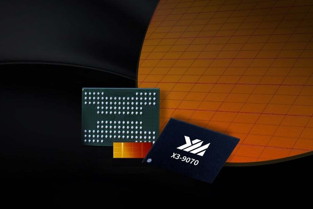
YMTC Starts Shipping 5th Generation NAND Flash with 294 Layers
Yangtze Memory Technologies Co. has begun shipping its fifth-generation 3D NAND memory chips, featuring 294 total layers and 232 active layers, according to an analysis from TechInsights. The new chips achieve bit density near 20 Gb per square millimeter (19.8 Gb/mm²), comparable to current offerings from SK Hynix and approaching Kioxia/Western Digital's latest products. YMTC's design uses hybrid bonding to connect the memory array with logic components, suggesting that Chinese memory makers are up to speed on the packaging standards that their non-sanctioned competitors use. The company has opted for a quiet release without formal announcements, a departure from typical industry practice. This low-key approach may be related to ongoing US trade restrictions on Chinese semiconductor companies.
While not setting records for active layers, SK Hynix's upcoming 321-layer chip leads in that metric, and YMTC's achievement in total layer count demonstrates continued technical progress. The chip uses string stacking technology, though the specific configuration of the layer arrays remains unclear. Other specifications show the new chip employs YMTC's Xtacking 4.0 architecture and triple-level cell (TLC) design. This matches major competitors' architecture type, though detailed performance metrics such as interface speeds have not been disclosed. The 5th generation NAND focuses on getting density on the right track. However, we expect YMTC to continue development at the same speed, match SK Hynix with 321-layer chips, and surpass it with Xtacking 5.0 in the near future.
While not setting records for active layers, SK Hynix's upcoming 321-layer chip leads in that metric, and YMTC's achievement in total layer count demonstrates continued technical progress. The chip uses string stacking technology, though the specific configuration of the layer arrays remains unclear. Other specifications show the new chip employs YMTC's Xtacking 4.0 architecture and triple-level cell (TLC) design. This matches major competitors' architecture type, though detailed performance metrics such as interface speeds have not been disclosed. The 5th generation NAND focuses on getting density on the right track. However, we expect YMTC to continue development at the same speed, match SK Hynix with 321-layer chips, and surpass it with Xtacking 5.0 in the near future.
Western Digital Reports Fiscal Second Quarter 2025 Financial Results
Western Digital Corp. today reported fiscal second quarter 2025 financial results.
"As we finalize the separation of our businesses, we are confident that both Western Digital and Sandisk will continue driving innovation and providing compelling storage solutions to customers while delivering long-term shareholder value," said David Goeckeler, Western Digital CEO. "We expect that our strong performance in HDD and our strategic approach to managing our Flash business within the New Era of NAND will allow each company to capture the growing demand for storage driven by the AI Data Cycle."


"As we finalize the separation of our businesses, we are confident that both Western Digital and Sandisk will continue driving innovation and providing compelling storage solutions to customers while delivering long-term shareholder value," said David Goeckeler, Western Digital CEO. "We expect that our strong performance in HDD and our strategic approach to managing our Flash business within the New Era of NAND will allow each company to capture the growing demand for storage driven by the AI Data Cycle."


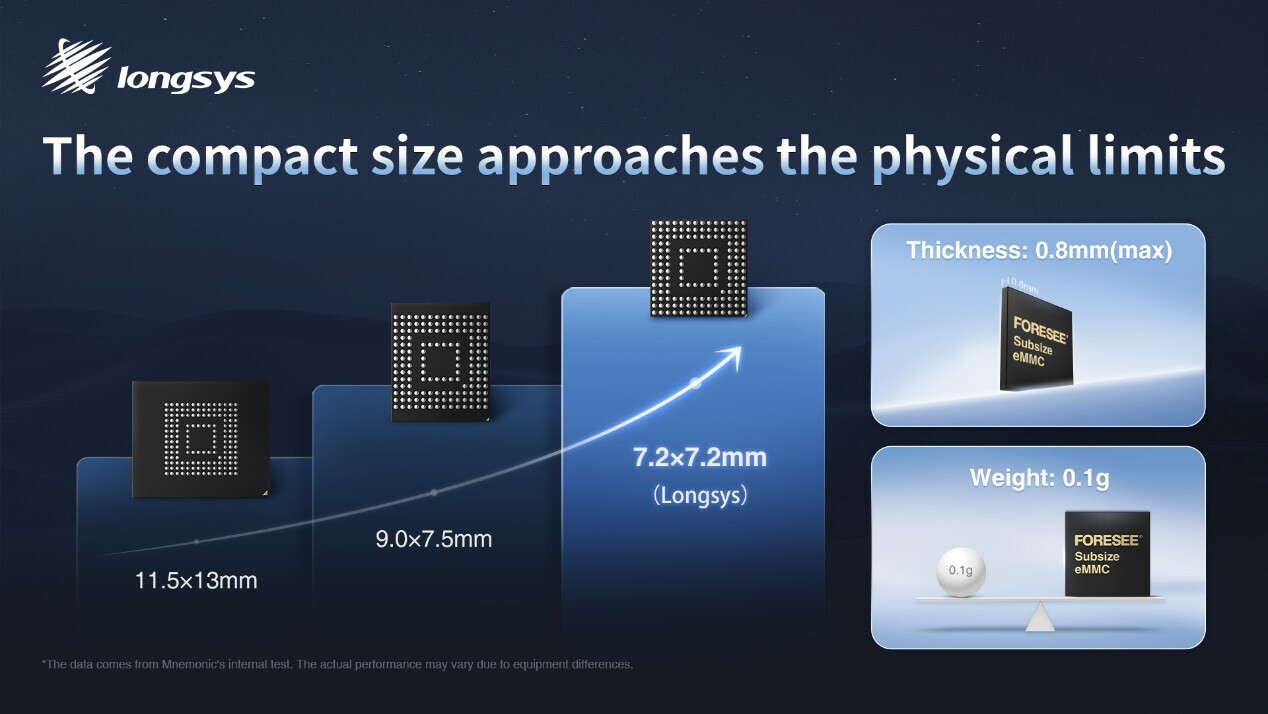
Longsys Launches 7.2mm Subsize eMMC, Breaking the Physical Space Constraints of AI Wearables
In the design of wearable devices, every millimeter matters. As AI technology becomes deeply integrated, wearable devices demand not only enhanced performance but also the ability to deliver more functionalities within highly limited spaces. Recently, Longsys introduced a 7.2 mm × 7.2 mm subsize eMMC, providing a groundbreaking memory solution for optimizing the physical space of AI wearables.
Ultra-Compact: Unlocking New Possibilities for Wearable Design
7.2 mm × 7.2 mm is one of the smallest subsize eMMCs currently available on the market, achieving maximum space efficiency. Its 153 solder balls nearly cover the entire panel, pushing the design to the very edge of physical limits. Compared to the standard 11.5 mm × 13 mm eMMC, its surface area is reduced by approximately 65%, with a thickness of just 0.8 mm. Featuring a lightweight design, it weighs only 0.1 g (approx.), nearly 67% lighter than the standard 0.3 g eMMC. This ultra-compact design frees up additional space for other internal components, enabling wearable devices to maintain a sleek and lightweight form while integrating more functional modules to meet diverse user demands.
NAND Flash Manufacturers to Resume Production Cuts in 2025 to Ease Supply-Demand Imbalance and Stabilize Prices
TrendForce's latest research report highlights that the NAND Flash industry will continue to face dual pressure from weak demand and oversupply in 2025. In response, manufacturers including Micron, Kioxia/SanDisk, Samsung, and SK hynix/Solidigm have similar plans to cut production—a move that could accelerate industry consolidation in the long term.
TrendForce reports that NAND Flash manufacturers are primarily implementing production cuts by lowering utilization rates and delaying process upgrades. These actions are driven by three major factors:
TrendForce reports that NAND Flash manufacturers are primarily implementing production cuts by lowering utilization rates and delaying process upgrades. These actions are driven by three major factors:


Kioxia at 2025 CES: 218-layer 3D NAND Flash and UFS 4.0 for Automotive Applications
Kioxia had a small dugout at the 2025 International CES. The NAND flash major tends to have a much bigger booth at FMS than CES. The one in Vegas had its latest enterprise SSDs, all of which were launched through 2024, and a couple of new things. We first got a practical demo of how Kioxia achieves 218 layers of NAND flash in its latest generation of BiCS Flash using an architectural innovation called CBA—CMOS directly bonded to array. In CBA, the cell array acts like a pizza topping to the crust that is the CMOS layer, rather than being arranged side-by-side. This allows for greater density of flash cells. This also has certain performance and power advantages.
Next up, the company showed us their automotive-grade UFS 4.0 non-volatile storage device, which uses the latest 218-layer 3D NAND flash memory. This device was announced toward the end of 2024, and gathered a salad of certifications that make it fit for the latest generation of automobiles with advanced technology such as FSD, or an infotainment system that's practically as powerful as a PC. We also got a fascinating look at the testbed Kioxia uses to validate its automotive UFS 4.0 devices.


Next up, the company showed us their automotive-grade UFS 4.0 non-volatile storage device, which uses the latest 218-layer 3D NAND flash memory. This device was announced toward the end of 2024, and gathered a salad of certifications that make it fit for the latest generation of automobiles with advanced technology such as FSD, or an infotainment system that's practically as powerful as a PC. We also got a fascinating look at the testbed Kioxia uses to validate its automotive UFS 4.0 devices.


Apr 16th, 2025 09:19 EDT
change timezone
Latest GPU Drivers
New Forum Posts
- Last game you purchased? (772)
- Help me identify Chip of this DDR4 RAM (20)
- 5070ti overclock...what are your settings? (5)
- Windows 11 fresh install to do list (23)
- How to relubricate a fan and/or service a troublesome/noisy fan. (229)
- GPU Memory Temprature is always high (16)
- Help For XFX RX 590 GME Chinese - Vbios (4)
- PCGH: "hidden site" to see total money spend on steam (3)
- Share your AIDA 64 cache and memory benchmark here (3053)
- NVFlash for RTX 50 Series (Blackwell) (0)
Popular Reviews
- G.SKILL Trident Z5 NEO RGB DDR5-6000 32 GB CL26 Review - AMD EXPO
- ASUS GeForce RTX 5080 TUF OC Review
- DAREU A950 Wing Review
- The Last Of Us Part 2 Performance Benchmark Review - 30 GPUs Compared
- Sapphire Radeon RX 9070 XT Pulse Review
- Sapphire Radeon RX 9070 XT Nitro+ Review - Beating NVIDIA
- Upcoming Hardware Launches 2025 (Updated Apr 2025)
- Thermaltake TR100 Review
- Zotac GeForce RTX 5070 Ti Amp Extreme Review
- TerraMaster F8 SSD Plus Review - Compact and quiet
Controversial News Posts
- NVIDIA GeForce RTX 5060 Ti 16 GB SKU Likely Launching at $499, According to Supply Chain Leak (182)
- NVIDIA Sends MSRP Numbers to Partners: GeForce RTX 5060 Ti 8 GB at $379, RTX 5060 Ti 16 GB at $429 (124)
- Nintendo Confirms That Switch 2 Joy-Cons Will Not Utilize Hall Effect Stick Technology (105)
- Over 200,000 Sold Radeon RX 9070 and RX 9070 XT GPUs? AMD Says No Number was Given (100)
- Nintendo Switch 2 Launches June 5 at $449.99 with New Hardware and Games (99)
- Sony Increases the PS5 Pricing in EMEA and ANZ by Around 25 Percent (85)
- NVIDIA PhysX and Flow Made Fully Open-Source (77)
- NVIDIA Pushes GeForce RTX 5060 Ti Launch to Mid-April, RTX 5060 to May (77)