News Posts matching #NAND flash

Return to Keyword Browsing

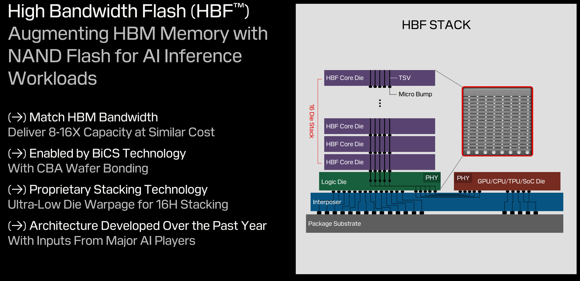
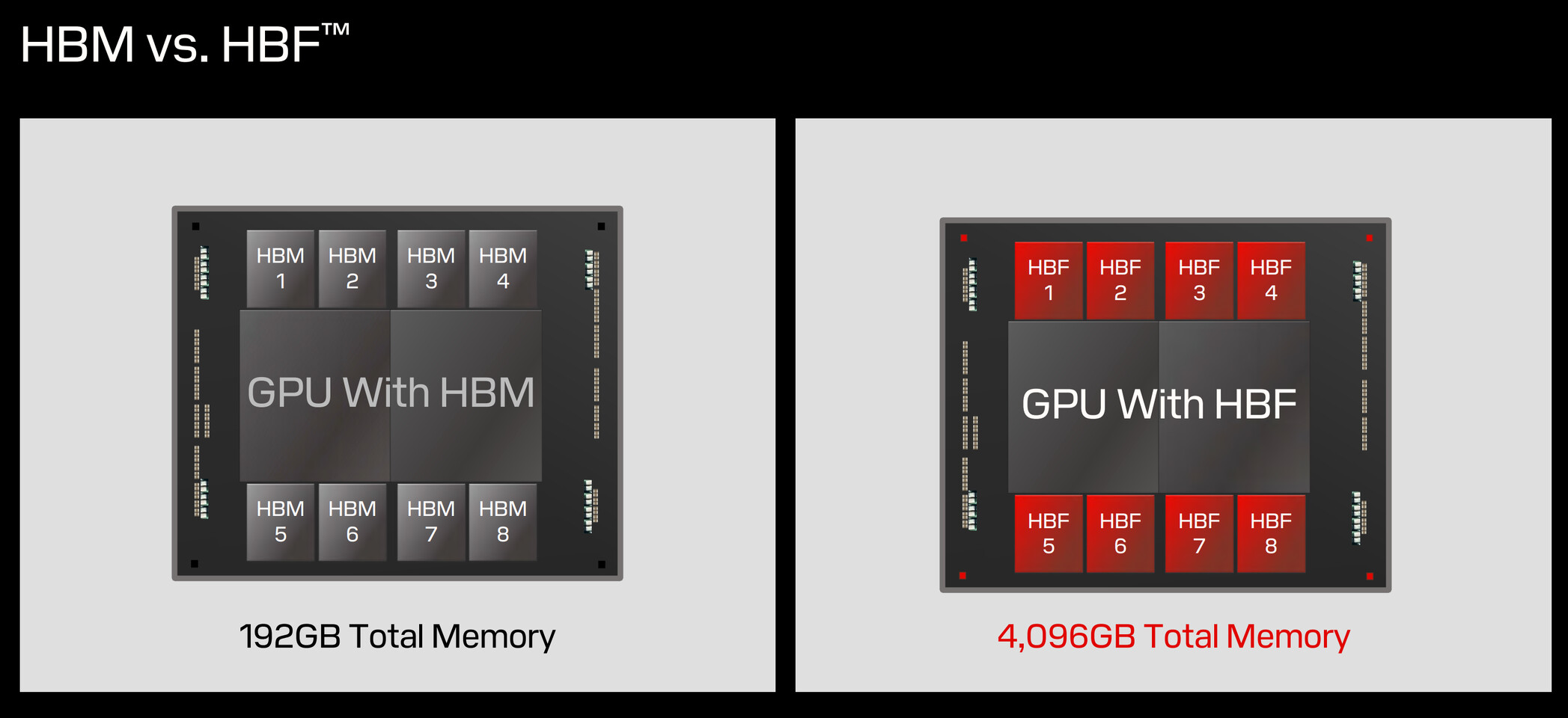
"DRAM+" Non-Volatile Memory Combines DRAM Speed With Flash Persistence

Ferroelectric Memory Co. (FMC) and Neumonda have formed a partnership to commercialize "DRAM+," a ferroelectric (FeRAM) memory architecture combining DRAM's speed with non-volatile data retention. The technology substitutes conventional capacitors with ferroelectric hafnium oxide (HfO₂) elements, allowing persistent storage without power while maintaining nanosecond access times. This hybrid technology addresses the performance gap between high-speed DRAM and storage-class memory like NAND flash. Unlike previous European DRAM ventures from Infineon and Qimonda that failed against commodity memory economics, FMC targets specialized applications valuing persistence and power efficiency. The HfO₂-based approach resolves limitations of previous FeRAM memory implementations using lead zirconate titanate (PZT) that couldn't scale beyond megabyte capacities.

Prototypes now demonstrate gigabit-range densities compatible with sub-10 nm fabrication of traditional DRAM made by Micron, Samsung, SK Hynix, and others. By eliminating refresh cycles, DRAM+ reduces static power consumption substantially compared to traditional one-transistor/one-capacitor DRAM cells. Primary applications include AI accelerators requiring persistent model weights, automotive ECUs with immediate startup requirements, and power-constrained medical implants. Neumonda will contribute its test platform suite Rhinoe, Octopus, and Raptor for electrical characterization and analytics at lower capital costs than standard semiconductor test equipment. No production timeline has been announced for commercial DRAM+ products.

Report Suggests that Samsung Will Increase DRAM & NAND Prices by 3 to 5%

Earlier today, industry moles in South Korea have heard whispers about Samsung Electronics planning a new pricing strategy for NAND and DRAM product lines. According to an MK news articles, local sources believe that company leadership will: "raise memory chip prices—by 3-5% from the current level—for major global customers. It is reported that some customers have already begun contract negotiations that reflect the increase conditions." Regional watchdogs posit that the megacorporation is reacting to very current geopolitical tensions (i.e. tariffs). Earlier this week, a main rival—Micron—informed customers about forthcoming memory price increases. Naturally, the North American memory chip giant is not "fully" affected by recent seismic shifts. A "significant growth demand" has caused jacked up charges—effective across DRAM, NAND flash, and HBM portfolios—projected throughout 2025 and 2026.

Returning to South Korean shores and Samsung, one unnamed semiconductor insider opined to MK: "oversupply continued throughout last year, but supply has recently decreased as major companies have begun to reduce production...In addition, artificial intelligence (AI) devices are appearing one after another in China, and demand for semiconductors is gradually increasing due to industrial automation." DRAMeXchange—an appropriately named market research organization—has kept track relevant trends. As disclosed by the MK news piece—as of last month, general-purpose DRAM DDR4 prices: "remained flat for the fourth month in a row." Looking at conditions for DDR5 (used in high-performance PCs and enterprise equipment), prices soared by 12%. DRAMeXchange observed NAND costs rising by 9.6%: "continuing an upward trend for the third consecutive month."

Micron Announces Memory Price Increases for 2025-2026 Amid Supply Constraints

In a letter to customers, Micron has announced upcoming memory price increases extending through 2025 and 2026, citing persistent supply constraints coupled with accelerating demand across its product portfolio. The manufacturer points to significant demand growth in DRAM, NAND flash, and high-bandwidth memory (HBM) segments as key drivers behind the pricing strategy. The memory market is rebounding from a prolonged oversupply cycle that previously depressed revenues industry-wide. Strategic production capacity reductions implemented by major suppliers have contributed to price stabilization and subsequent increases over the past twelve months. This pricing trajectory is expected to continue as data center operators, AI deployments, and consumer electronics manufacturers compete for limited memory allocation.

In communications to channel partners, Micron emphasized AI and HPC requirements as critical factors necessitating the price adjustments. The company has requested detailed forecast submissions from partners to optimize production planning and supply chain stability during the constrained market period. With its pricing announcement, Micron disclosed a $7 billion investment in a Singapore-based HBM assembly facility. The plant will begin operations in 2026 and will focus on HBM3E, HBM4, and HBM4E production—advanced memory technologies essential for next-generation AI accelerators and high-performance computing applications from NVIDIA, AMD, Intel, and other companies. The price increases could have cascading effects across the AI and GPU sector, potentially raising costs for products ranging from consumer gaming systems to enterprise data infrastructure. We are monitoring how these adjustments will impact hardware refresh cycles and technology adoption rates as manufacturers pass incremental costs to end customers.

Intel to Receive $1.9 Billion as SK Hynix Finalizes NAND Deal

Intel and SK Hynix have finalized an $8.85 billion transaction involving Intel's NAND flash memory operations, marking the conclusion of a two-phase deal initiated in 2020. In the first phase of the transaction, SK Hynix acquired Intel's SSD division along with a NAND production facility in Dalian, China, for $6.61 billion. The Dalian facility was later rebranded as Solidigm. Notably, this phase transferred only the physical assets and operational facilities, leaving behind critical intellectual property, research and development infrastructure, and specialized technical staff. The second phase, finalized with a payment of $1.9 billion this Tuesday, addressed these remaining components. With this payment, SK Hynix secured full rights to Intel's proprietary NAND technology, R&D resources, and the technical workforce dedicated to NAND operations.

During the transition period, Intel maintained control over these elements, which limited integration between Solidigm and Intel's NAND teams. This separation was designed to manage operational risks and gradually transfer capabilities. Completing this deal helps with a strategic restructuring of Intel's portfolio as it shifts focus toward high-growth areas such as AI chip development, foundry services, and next-generation semiconductor manufacturing. A $1.9 billion financial injection is perfect in time for Intel Foundry business, burning billions per year, to offset some of the losses. For SK Hynix, consolidating the complete range of Intel's NAND operations enhances its competitive position in the global NAND market, providing access to established technologies and key industry expertise. This finalization is part of a broader trend where companies divest from commoditized memory products to concentrate on more advanced semiconductor solutions like AI chips and other accelerators, which are enjoying higher margins and a better business outlook.

Phison Expands aiDAPTIV+ GPU Memory Extension Capabilities

Phison Electronics (8299TT), a leading innovator in NAND flash technologies, today announced an array of expanded capabilities on aiDAPTIV+, the affordable AI training and inferencing solution for on-premises environments. aiDAPTIV+ will be integrated into a ML-series Maingear laptop, the first AI laptop PC capable of LLMOps, utilizing NVIDIA GPUs and available for concept demonstration and registration this week at NVIDIA GTC 2025. Customers will be able to fine-tune Large Language Models (LLMs) up to 8 billion parameters using their own data.

Phison also expanded aiDAPTIV+ capabilities to run on edge computing devices powered by the NVIDIA Jetson platform, for enhanced generative AI inference at the edge and robotics deployments. With today's announcement, new and current aiDAPTIV+ users can look forward to the new aiDAPTIVLink 3.0 middleware, which will provide faster Time to First Token (TTFT) recall and extend the token length for greater context, improving inferencing performance and accuracy. These expansions will unlock access for users ranging from university students and AI industry professionals learning to train LLMs, or researchers uncovering deeper insights within their own data using a PC, all the way to manufacturing engineers automating factory floor enhancements via edge devices.

Silicon Motion Announces PCIe Gen5 Enterprise SSD Reference Design Kit Supporting up to 128TB

Silicon Motion Technology Corporation ("Silicon Motion"), a global leader in designing and marketing NAND flash controllers for solid-state storage devices, today announced the sampling of its groundbreaking MonTitan SSD Reference Design Kit (RDK) that supports up to 128 TB with QLC NAND. Designed on the advanced MonTitan PCIe Gen 5 SSD Development Platform. This new offering aims to accelerate enterprise and data center storage AI SSD solutions by providing a robust and efficient RDK for OEMs and partners.

The SSD RDK incorporates Silicon Motion's PCIe Dual Ported enterprise-grade SM8366 controller, which supports PCIe Gen 5 x4 NVMe 2.0 and OCP 2.5 data center specifications offering unmatched performance, QoS, and capacity for next-generation large data lake storage needs.

Kingston Debuts DC3000ME PCIe 5.0 NVMe U.2 Enterprise SSD with eTLC NAND

Kingston has introduced its new DC3000ME line of enterprise-grade PCIe 5.0 SSDs. These top-tier storage devices come in a U.2 15 mm form factor (100.50 mm × 69.8 mm × 14.8 mm) and use 3D eTLC NAND flash memory. The drives include built-in power loss protection and AES 256-bit hardware-based encryption. Kingston DC3000ME SSDs are designed for server applications such as AI, HPC, OLTP, databases, cloud infrastructure, and edge computing. As an enterprise-grade product, the DC3000ME SSDs also feature various built-in telemetry such as media wear, temperature, health, etc.

At this moment, they are offered in three sizes: 3.84 TB, 7.68 TB, and 15.36 TB. Each version has 1DWPD durability with a 5-year warranty. In terms of power consumption, we have 8 W when idle and up to 24 W during writing operations. Kingston points out the drives' steady I/O performance and quick response times, with read delays under 10µs at 99% and write delays under 70µs. (up to 14,000/10,000 MB/s sequential read/write and up to 2,800,000/500,000 4k random read/write IOPS). The drives also have NVMe-MI 1.2b remote management, end-to-end data safety, and support for TCG Opal 2.0. Exact pricing is still to be announced, however we found them online at €686,9 (3.84 TB), €1226,9 (7.68 TB), €2252,9 (15.36 TB).

Silicon Motion Showcases Storage Solutions for AI and Display Interface SoCs at Embedded World 2025

Silicon Motion Technology Corporation, a global leader in NAND flash controllers for solid-state storage devices, today announced its participation in Embedded World 2025, taking place from March 11-13, 2025, in Nuremberg, Germany.

At the event, Silicon Motion will showcase its latest storage and display interface solutions, including PCIe NVMe Gen 4/5 SSD controllers, Ferri embedded storage solutions, and advanced display interface SoCs. These cutting-edge innovations are designed to maximize performance per watt, extend device longevity and power for the next generation of AI-driven industrial, embedded, automotive, and data center applications.

Advantech Launches the SQFlash EDSFF and EU-2 PCIe Gen5 x4 SSDs

Advantech, a global leader in industrial flash storage solutions, introduces the SQFlash EDSFF and EU-2 PCIe Gen 5 x4 SSDs, designed to meet the demands of next-generation enterprise and data center applications. Till 2024, PCIe Gen 4 solutions accounted for 50% of the market, and PCIe Gen 5 products are rapidly gaining traction across diverse applications. Among PCIe storage products, form factors such as U.2, E3.S, and E1.S are driving market growth.

The SQFlash E1.S SSD, built on the EDSFF standard, delivers exceptional performance with PCIe Gen 5 read and write speeds of up to 14,000 MB/s and 8,500 MB/s, respectively, while offering scalability, power efficiency, and thermal optimization. Meanwhile, the SQFlash EU-2 PCIe Gen.5 x4 SSD leverages cutting-edge PCIe 5.0 technology, setting new standards in speed, reliability, and thermal management, making it ideal for data centers, enterprise computing, real-time analytics, and AI-driven workloads.

Reports Suggest SK hynix Finalizing Acquisition of Intel NAND Business

Almost five years ago, SK hynix announced a planned $9 billion acquisition of Intel's NAND flash memory and storage business. The semiconductor giant's takeover process has been a gradual affair; the first phase was complete by the end of 2021, with Asian governing bodies—just before Christmas—giving clearance to absorb Chinese facilities. Within this time frame, the South Korean giant pulled in Team Blue's SSD NAND design and R&D departments—thus establishing the "Solidigm" entity. According to a new Businesskorea report, SK hynix is about to pay off a final installment; allegedly $2.235 billion.

Industry insiders believe that SK hynix's takeover of Intel NAND and storage properties will be completed by next month. This (rumored) March time fortification will place SK hynix in direct competition with a nearby rival: Samsung. Businesskorea believes that recent expansions signal a "competitive edge"—targeting increased demand for enterprise SSD products. Google and Meta are reportedly engaged in widespread upgrading of data center facilities. The local publication reckons that: "SK Hynix plans to capitalize on this trend by strengthening its position in the market and leveraging AI to drive innovation and growth." The aforementioned absorption of Intel intellectual property (IP) plus R&D resources is viewed as a crucial move in reinforcing an already solid foundation.

Numemory Releases Optane Successor: "NM101" Storage-Class Memory

Numemory has introduced the NM101, a 64 Gb storage-class memory module that uses technology similar to Intel's now-discontinued Optane architecture. The device implements phase-change memory and crossbar technology in a 3D selector-only memory structure, matching Optane's 3200 MT/s transfer rate specification. The technical architecture diverges from Intel's implementation by using a single selector in its cross-point structure rather than the dual-selector approach of 3D XPoint memory. Operating at 1.2 V with an X8 bus width, the NM101 uses 3D stacking to achieve claimed performance metrics of 10x faster read/write speeds than NAND flash. Xincun Technology, which established the Numemory division in Wuhan in 2022, holds 273 patents related to the technology, including 60 international and 213 Chinese patents. The company's R&D team of 144 engineers has developed the architecture since 2019, three years before Intel ended its Optane program.

Production plans specify an initial manufacturing target of 10,000 units monthly by the end of 2025. Guao Technology has committed ¥10 billion to establish production facilities in Zhejiang province, with additional funding from the Anji county government. The NM101's operating temperature range spans 0-70°C, suitable for standard data center environments. While the device's specifications suggest the potential for data center deployment, specific IOPS and latency metrics remain unpublished. Initial production will serve domestic Chinese servers and storage manufacturers. The technology's viability in mass production remains to be demonstrated, particularly given the manufacturing challenges that contributed to Optane's market exit. The Chinese internal market is massive, so serving only domestic companies could be enough for Numemory at the beginning. If the company continues development, worldwide expansion could pick up where Optane stopped.

Kioxia and Sandisk Unveil Next-Generation 3D Flash Memory Technology Achieving 4.8Gb/s NAND Interface Speed

Kioxia Corporation and Sandisk Corporation have pioneered a state-of-the-art 3D flash memory technology, setting the industry benchmark with a 4.8 Gb/s NAND interface speed, superior power efficiency, and heightened density

Unveiled at ISSCC 2025, the new 3D flash memory innovation, together with the companies' revolutionary CBA (CMOS directly Bonded to Array) technology, incorporates one of the latest interface standards, Toggle DDR6.0 for NAND flash memory, and leverages the SCA (Separate Command Address) protocol, a novel command address input method of its interface, and PI-LTT (Power Isolated Low-Tapped Termination) technology, which is instrumental in further reducing power consumption.

SanDisk Develops HBM Killer: High-Bandwidth Flash (HBF) Allows 4 TB of VRAM for AI GPUs

During its first post-Western Digital spinoff investor day, SanDisk showed something it has been working on to tackle the AI sector. High-bandwidth flash (HBF) is a new memory architecture that combines 3D NAND flash storage with bandwidth capabilities comparable to high-bandwidth memory (HBM). The HBF design stacks 16 3D NAND BiCS8 dies using through-silicon vias, with a logic layer enabling parallel access to memory sub-arrays. This configuration achieves 8 to 16 times greater capacity per stack than current HBM implementations. A system using eight HBF stacks can provide 4 TB of VRAM to store large AI models like GPT-4 directly on GPU hardware. The architecture breaks from conventional NAND design by implementing independently accessible memory sub-arrays, moving beyond traditional multi-plane approaches. While HBF surpasses HBM's capacity specifications, it maintains higher latency than DRAM, limiting its application to specific workloads.

SanDisk has not disclosed its solution for NAND's inherent write endurance limitations, though using pSLC NAND makes it possible to balance durability and cost. The bandwidth of HBF is also unknown, as the company hasn't put out details yet. SanDisk Memory Technology Chief Alper Ilkbahar confirmed the technology targets read-intensive AI inference tasks rather than latency-sensitive applications. The company is developing HBF as an open standard, incorporating mechanical and electrical interfaces similar to HBM to simplify integration. Some challenges remain, including NAND's block-level addressing limitations and writing endurance constraints. While these factors make HBF unsuitable for gaming applications, the technology's high capacity and throughput characteristics align with AI model storage and inference requirements. SanDisk has announced plans for three generations of HBF development, indicating a long-term commitment to the technology.

Plasma Technology Doubles Etch Rate for 3D NAND Flash Memory

Scientists have made a big step forward in data storage technology, they've managed to improve the manufacturing process for 3D NAND flash memory. This type of storage technology stacks memory cells on top of each other to obtain higher data density. A team of experts from Lam Research, the University of Colorado Boulder, and Princeton Plasma Physics Lab came up with a better way to etch (the process of carving holes into alternating layers of silicon oxide and silicon nitride) by using hydrogen fluoride plasma. This new method cuts vertical channels through silicon-based materials twice as fast as before achieving 640 nanometers in just one minute.

The team found out that mixing in certain chemicals like phosphorus trifluoride helps the etching process. They also learned that some byproducts can slow down etching, but adding water can help fix this problem. "The salt can decompose at a lower temperature when water is present, which can accelerate etching", said Yuri Barsukov, a former PPPL researcher now working at Lam Research. This breakthrough is important as the need for data storage received a huge boost with the rise of AI programs, that need tons of storage.

Kioxia at 2025 CES: 218-layer 3D NAND Flash and UFS 4.0 for Automotive Applications

Kioxia had a small dugout at the 2025 International CES. The NAND flash major tends to have a much bigger booth at FMS than CES. The one in Vegas had its latest enterprise SSDs, all of which were launched through 2024, and a couple of new things. We first got a practical demo of how Kioxia achieves 218 layers of NAND flash in its latest generation of BiCS Flash using an architectural innovation called CBA—CMOS directly bonded to array. In CBA, the cell array acts like a pizza topping to the crust that is the CMOS layer, rather than being arranged side-by-side. This allows for greater density of flash cells. This also has certain performance and power advantages.

Next up, the company showed us their automotive-grade UFS 4.0 non-volatile storage device, which uses the latest 218-layer 3D NAND flash memory. This device was announced toward the end of 2024, and gathered a salad of certifications that make it fit for the latest generation of automobiles with advanced technology such as FSD, or an infotainment system that's practically as powerful as a PC. We also got a fascinating look at the testbed Kioxia uses to validate its automotive UFS 4.0 devices.

Micron at the 2025 CES: Scripting a Strong Comeback to the Client and PC-DIY Segments

Micron at the 2025 International CES showed us product that hint at the company planning a strong comeback to the client and PC-DIY market segments. The company's Crucial brand is already a high-volume player in the client segment, but the company never really approached the enthusiast segment. Products like the company's new T705 Pro and P510 NVMe SSDs, and DDR5 Pro Overclocking memory, seek to change this. We begin our tour with PC memory, and the DDR5 Pro OC CUDIMMs. Crucial has jumped onto the CKD bandwagon, introducing memory modules and kits that come with DDR5-6400 out of the box, but which are geared for manual overclocking to take advantage of the 1β DRAM chips underneath (hence the name).

The company also showed us their first DDR5 CSODIMM suitable for the next generation of notebooks with HX-segment processors. This module comes with a CKD and a DDR5-6400 JEDEC-standard SPD profile out of the box. Lastly, there's the Micron-branded LPCAMM2, which comes in speeds of up to LPDDR5X-8533, and is suitable for the next generation of ultraportables.

From AI to IoT: KIOXIA Highlights Flash Memory Solutions for an Unlimited Array of End User Applications at CES 2025

This week at CES 2025, KIOXIA America, Inc. will highlight the transformative potential of flash memory. As pioneers of NAND flash technology, KIOXIA will demonstrate how its innovative solutions empower users to achieve more, tackle challenges, and unlock creativity—making everyday moments and groundbreaking innovations possible.

Visitors to the KIOXIA exhibit will discover how flash memory is redefining storage for a digital-first world. The company will showcase cutting-edge solutions for diverse industries, from memory and SSDs for artificial intelligence and automotive to flash products for consumer and industrial applications.

Phison Shows Off 6nm E28 NVMe Gen 5 Controller; E31T with Micron G9, and a Massive Enterprise SSD

At CES 2025, we found the SSD controller that will spur high-end NVMe Gen 5 SSD adoption. Until now, high-end Gen 5 SSDs were driven by Phison's E26 series controller that the company built on TSMC's 12 nm process. The company on Monday launched the new E28 series controller (full name PS5028-E28). This chip is built on the much more advanced TSMC 6 nm process. The new process lets Phison to significantly lower the electrical cost of its NAND flash interface serializer-deserializer, and step up performance closer to the interface limits of PCI-Express 5.0 x4. The controller offers sequential speeds of up to 14.5 GB/s, which is an increase from last year's E26 Max14um variant.

The company showed us the bare E28 controller chip, and a reference-design SSD based on it. Not much to report, except that the drive lacked any cooling solution. Production SSDs powered by the E28 will still need heatsinks to achieve optimal performance, although they won't run as hot as drives powered by the E26. The company didn't have any performance demo stations set up with this drive.

Transcend Unveils Enterprise SSD to Boost Data Center Performance and Security

Transcend Information Inc. (Transcend) a global leader in storage solutions, introduces the new ETD210T enterprise 2.5-inch SSD, designed to meet the read-intensive needs of business users. Featuring enterprise-grade TLC (eTLC) NAND flash and a SATA III 6 Gb/s interface, the ETD210T includes a built-in DRAM cache to deliver fast data transfer, exceptional Quality of Service (QoS), ultra-low latency, and superior endurance. Ideal for read-intensive and high-capacity storage workloads in cloud and data center applications, it provides a reliable and efficient storage solution for enterprise computing.

Designed for Enterprises, Optimized for Data Centers
The ETD210T supports various enterprise applications, including data centers, virtualized servers, and large-scale data processing. Equipped with high-endurance eTLC NAND flash, it delivers exceptional read and write performance. Its endurance rating of DWPD = 1 meets the requirements of most enterprise-class applications, while its read and write speeds of up to 530 MB/s and 510 MB/s, respectively, address the need for highly efficient storage.

YMTC Produces up to 500,000 Wafers Per Year of Leading-Edge NAND Memory

Chinese semiconductor memory giant YMTC is reportedly manufacturing anywhere between 400-500,000 wafers per year of leading-edge NAND memory, all on domestically produced wafers. According to Mayuki Hashimoto, CEO and Chairman of SUMCO, a Japanese company supplying raw silicon ingots and polished wafers, they are seeing a significant business impact stemming from China's growing self-reliance, especially with companies like YMTC producing its own silicon ingots and polished wafers. This has led to SUMCO's decreasing revenue, where the CEO shared some insights about Chinese ambitions. He added that China is producing about one million wafers of silicon per year, most of which are test wafers. This includes test runs from companies like SMIC and its customers, such as T-Head, HiSilicon, and others.

Last year, YMTC, with its Xtacking 4.0 3D NAND flash architecture, was the first company to achieve a 200+ layer count in the 3D NAND space. The company's product, X4-9070, a 232-layer TLC 3D NAND, uses multiple silicon wafers, hence growing its massive consumption of silicon that is projected to reach 500,000 wafers per year. Given that this is all homegrown silicon from ingots to NAND, this is a massive success for Chinese self-reliance efforts but a huge blow to companies that used to supply Chinese firms with raw materials. Although the company uses custom silicon, it still relies on foreign tools, photoresists, and pre-cursors. There are some indications that YMTC is developing its own tools; it is a plan of a broader strategy in the Chinese semiconductor industry to develop every step of the semiconductor manufacturing process. Huawei is also there to develop EUV scanners, and YMTC could help with its memory business, which is in need of a new tool.

JEDEC Announces Enhanced NAND Flash Interface Standard With Increased Speeds and Efficiency

JEDEC Solid State Technology Association, the global leader in the development of standards for the microelectronics industry, today announced the publication of JESD230G: NAND Flash Interface Interoperability Standard. JESD230G introduces speeds of up to 4800 MT/s, as compared to 400 MT/s in the first version of JESD230 published in 2011. Also, JESD230G adds a separate Command/Address Bus Protocol (SCA), delivering enhanced throughput and efficiency by allowing hosts and NAND devices to take maximum advantage of the latest interface speeds. JESD230G is available for free download from the JEDEC website.

"JEDEC is excited to release JESD230G," said David Landsman, Distinguished Engineer at Western Digital and Chair of the JEDEC NAND TG. He added, "This version of JESD230 further advances the capabilities of NAND flash devices to meet the growing demands of their expanding range of applications and continues the JEDEC tradition of building interoperable ecosystems through open industry standards."

Transcend Introduces CFast Card With Write Protection for Enhanced Data Security

Transcend Information Inc. (Transcend ), a leading global manufacturer of memory storage solutions, announces the launch of its new CFX735 and CFX735I CFast cards. These cards feature built-in write protection technology, designed specifically for professional applications that require secure data storage and stable, high-performance write capabilities.

Leveraging 112-layer 3D NAND flash technology and a SATA III 6 Gb/s interface, this series offers exceptional read/write speeds and large storage capacities. Whether you're dealing with data-intensive applications or operating in demanding environments, these cards deliver reliable performance. The CFX735 operates in a temperature range of -5°C to 70°C, while the CFX735I is built for extreme environments, functioning reliably from -40°C to 85°C, perfect for outdoor and temperature fluctuating scenarios.

Solidigm Launches D5-P5336 PCIe Data Center SSDs With 122 TB Capacity

Solidigm, a leading provider of innovative NAND flash memory solutions, announced today the introduction of the world's highest capacity PCIe solid-state drive (SSD): the 122 TB (terabyte) Solidigm D5-P5336 data center SSD. The D5-P5336 doubles the storage space of Solidigm's earlier 61.44 TB version of the drive and is the world's first SSD with unlimited Random Write endurance for five years—offering an ideal solution for AI and data-intensive workloads. Just how much storage is 122.88 TB? Roughly enough for 4K-quality copies of every movie theatrically released in the 1990s, 2.6 times over.

Data storage power, thermal and space constraints are accelerating as AI adoption increases. Power and space-efficient, the new 122 TB D5-P5336 delivers industry-leading storage efficiency from the core data center to the edge. Data center operators can deploy with confidence the 122 TB D5-P5336 from Solidigm, the proven QLC (quad-level cell) density leader with more than 100EB (exabytes) of QLC-based product shipped since 2018.

Apple's New Mac mini Comes with Removable Storage

Both pictures and videos of a partial teardown of Apple's recently launched Mac mini with the M4 SoC have appeared online courtesy of various Chinese sources. There are at least two interesting parts to these partial teardowns and they're related to storage and WiFi. On the storage front, Apple has moved away from having soldered NAND chips straight on the main PCB of the Mac mini, to instead having them on a custom PCB which is similar to M.2, but a custom Apple design. The PCB pictured contained a pair of 128 GB NAND chips and with the source of the teardown being from China, there's also a video showing a repair shop desoldering the two chips and replacing them with two 1 TB chips, or in other words, the SSD was upgraded from 256 GB to 2 TB.

The upgrade brought with it some extra performance as well, even if the write speed remained at a comparatively slow 2900 MB/s, the read speed went up from 2000 MB/s to 3300 MB/s which is a significant gain in performance. This is obviously not a consumer friendly upgrade path, but we'd expect to see third party upgrade options at some point in the future, assuming there's no black listing of third party storage modules. The NAND controller is still likely to be integrated into Apple's SoC, but the PCB that the NAND flash chips are mounted onto appears to have some kind of SPI flash on it as well, which might make third party upgrades a lot harder.

Samsung Plans 400-Layer V-NAND for 2026 and DRAM Technology Advancements by 2027

Samsung is currently mass-producing its 9th generation V-NAND flash memory chips with 286 layers unveiled this April. According to the Korean Economic Daily, the company targets V-NAND memory chips with at least 400 stacked layers by 2026. In 2013, Samsung became the first company to introduce V-NAND chips with vertically stacked memory cells to maximize capacity. However, stacking beyond 300 levels proved to be a real challenge with the memory chips getting frequently damaged. To address this problem, Samsung is reportedly developing an improved 10th-generation V-NAND that is going to use the Bonding Vertical (BV) NAND technology. The idea is to manufacture the storage and peripheral circuits on separate layers before bonding them vertically. This is a major shift from the current Co-Packaged (CoP) technology. Samsung stated that the new method will increase the density of bits per unit area by 1.6 times (60%), thus leading to increased data speeds.

Samsung's roadmap is truly ambitious, with plans to launch the 11th generation of NAND in 2027 with an estimated 50% improvement in I/O rates, followed by 1,000-layer NAND chips by 2030. Its competitor, SK hynix, is also working on 400-layer NAND aiming to have the technology ready for mass production by the end of 2025, as we previously mentioned in August. Samsung, the current HBM market leader with a 36.9% market share have also plans for its DRAM sector intending to introduce the sixth-generation 10 nm DRAM, or 1c DRAM by the first half of 2025. Then we can expect to see Samsung's seventh-generation 1d nm (still on 10 nm) in 2026, and by 2027 the company hopes to release its first generation sub-10 nm DRAM, or 0a DRAM memory that will use a Vertical Channel Transistor (VCT) 3D structure similar to what NAND flash utilizes.
Return to Keyword Browsing
Apr 22nd, 2025 10:21 EDT change timezone

New Forum Posts

Popular Reviews

Controversial News Posts