Rapidus Confirms Launching 2nm Pilot Line in April, Mass Production Set for 2027
Rapidus Corporation today announced that its plans and budget for fiscal year 2025 have been approved by Japan's New Energy and Industrial Technology Development Organization (NEDO). The approval covers two commissioned projects under NEDO's "Post-5G Information and Communication Systems Infrastructure Enhancement R&D Project / Development of Advanced Semiconductor Manufacturing Technology (Commissioned)." These projects are the "Research and Development of 2 nm-Generation Semiconductor Integration Technology and short TAT (turnaround time) Manufacturing Technology Based on Japan-U.S. Collaboration" and "Development of Chiplet, Package Design and Manufacturing Technology for 2 nm-Generation Semiconductors."
The first of these projects, focused on front-end processes, was launched in November 2022 as part of Japan's next-generation semiconductor R&D effort. Under this program, Rapidus has continued construction of the Innovative Integration for Manufacturing (IIM) facility in Chitose, Hokkaido, which will serve as its production base. It also sent engineers to IBM in the U.S. to jointly develop 2 nm logic semiconductor mass production technologies and continued to achieve target performance as planned. Furthermore, Rapidus has installed EUV lithography and other production equipment at the IIM facility, and started cleanroom operation. As a result of these efforts, the company achieved its performance targets for FY2024.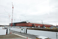

The first of these projects, focused on front-end processes, was launched in November 2022 as part of Japan's next-generation semiconductor R&D effort. Under this program, Rapidus has continued construction of the Innovative Integration for Manufacturing (IIM) facility in Chitose, Hokkaido, which will serve as its production base. It also sent engineers to IBM in the U.S. to jointly develop 2 nm logic semiconductor mass production technologies and continued to achieve target performance as planned. Furthermore, Rapidus has installed EUV lithography and other production equipment at the IIM facility, and started cleanroom operation. As a result of these efforts, the company achieved its performance targets for FY2024.


