Mar 26th, 2025 08:58 EDT
change timezone
Latest GPU Drivers
New Forum Posts
- The TPU UK Clubhouse (25959)
- Packing Ties vs. Cable/Zip Ties (2)
- Should you physically remove secondary NVMe drives when performing a clean Windows install? (8)
- Windows 10 Vs 11, Which one too choose? (104)
- Discussion: linux-6.14.X (10)
- Recommended PhysX card for 5xxx series? [Is vRAM relevant?] (220)
- Is RX 9070 VRAM temperature regular value or hotspot? (208)
- any alternative to razer synapse to adjust mouse settings (5)
- What features do you want to see in a first person survival horror game? (40)
- HP Workstations Owners Club (377)
Popular Reviews
- Assassin's Creed Shadows Performance Benchmark Review - 30 GPUs Compared
- be quiet! Pure Rock Pro 3 Black Review
- ASUS ProArt X870E-Creator Wi-Fi Review
- ASRock Radeon RX 9070 XT Taichi OC Review - Excellent Cooling
- Pulsar Feinmann F01 Review
- Sapphire Radeon RX 9070 XT Nitro+ Review - Beating NVIDIA
- ASRock Phantom Gaming B860I Lightning Wi-Fi Review
- ASUS GeForce RTX 5070 TUF OC Review
- AMD Ryzen 9 9950X3D Review - Great for Gaming and Productivity
- AMD Ryzen 7 9800X3D Review - The Best Gaming Processor
Controversial News Posts
- AMD RDNA 4 and Radeon RX 9070 Series Unveiled: $549 & $599 (260)
- AMD Radeon RX 9070-series Pricing Leaks Courtesy of MicroCenter (158)
- MSI Doesn't Plan Radeon RX 9000 Series GPUs, Skips AMD RDNA 4 Generation Entirely (142)
- Microsoft Introduces Copilot for Gaming (123)
- AMD Radeon RX 9070 XT Reportedly Outperforms RTX 5080 Through Undervolting (118)
- NVIDIA Reportedly Prepares GeForce RTX 5060 and RTX 5060 Ti Unveil Tomorrow (115)
- Over 200,000 Sold Radeon RX 9070 and RX 9070 XT GPUs? AMD Says No Number was Given (100)
- NVIDIA GeForce RTX 5050, RTX 5060, and RTX 5060 Ti Specifications Leak (96)
News Posts matching #Tokyo Electron
Return to Keyword BrowsingUS to Implement Semiconductor Restrictions on Chinese Equipment Makers
The Biden administration is set to announce new, targeted restrictions on China's semiconductor industry, focusing primarily on emerging chip manufacturing equipment companies rather than broad industry-wide limitations. According to Bloomberg, these new restrictions are supposed to take effect on Monday. The new rules will specifically target two manufacturing facilities owned by Semiconductor Manufacturing International Corp. (SMIC) and will add select companies to the US Entity List, restricting their access to American technology. However, most of Huawei's suppliers can continue their operations, suggesting a more mild strategy. The restrictions will focus on over 100 emerging Chinese semiconductor equipment manufacturers, many of which receive government funding. These companies are developing tools intended to replace those currently supplied by industry leaders such as ASML, Applied Materials, and Tokyo Electron.
The moderated approach comes after significant lobbying efforts from American semiconductor companies, who argued that stricter restrictions could disadvantage them against international competitors. Major firms like Applied Materials, KLA, and Lam Research voiced concerns about losing market share to companies in Japan and the Netherlands, where similar but less stringent export controls are in place. Notably, Japanese companies like SUMCO are already seeing the revenue impacts of Chinese independence. Lastly, the restrictions will have a limited effect on China's memory chip sector. The new measures will not directly affect ChangXin Memory Technologies (CXMT), a significant Chinese DRAM manufacturer capable of producing high-bandwidth memory for AI applications.
The moderated approach comes after significant lobbying efforts from American semiconductor companies, who argued that stricter restrictions could disadvantage them against international competitors. Major firms like Applied Materials, KLA, and Lam Research voiced concerns about losing market share to companies in Japan and the Netherlands, where similar but less stringent export controls are in place. Notably, Japanese companies like SUMCO are already seeing the revenue impacts of Chinese independence. Lastly, the restrictions will have a limited effect on China's memory chip sector. The new measures will not directly affect ChangXin Memory Technologies (CXMT), a significant Chinese DRAM manufacturer capable of producing high-bandwidth memory for AI applications.

China Bought More Chipmaking Tools in the First Half of 2024 Than US, Taiwan, and South Korea Combined
According to a recent report from Nikkei, China has claimed the number one spot as the single highest spender on chipmaking tools. As the data from SEMI highlights, China spent a whopping $25 billion on key semiconductor tools in the first half of 2024, more than the US, Taiwan, and South Korea combined. And the train of acceleration for the Chinese semiconductor industry doesn't seem to be slowing down, as the country is expected to spend more than $50 billion for the entire year 2024. However, this equipment is not precisely leading-edge, as Chinese companies are under Western sanctions and are unable to source advanced EUV lithography tools for making sub-7 nm chips.
Most of the spending is allocated to mature node chipmaking facilities. These so-called "second tier" companies are driving the massive expenditures, and they are plentiful. Nikkei reports that there are at least ten firms that operate with mature nodes like 10/12/16 nm nodes. Being the biggest spender, China is also one of the primary revenue sources for many companies. For the US chipmaking tool companies like Applied Materials, Lam Research, and KLA, Chinese purchases accounted for 32%, 39%, and 44% of their latest quarterly revenue, respectively. Tokyo Electron recorded orders to China accounting for 49.9% of its revenues in June, while the Netherlands giant ASML also attributed 49%. Perhaps even more interesting is the expected outlook for 2025, which shows no signs of slowing down. The Chinese semiconductor industry must establish complete self-sufficiency, and massive capital expenditures are expected to continue.
Most of the spending is allocated to mature node chipmaking facilities. These so-called "second tier" companies are driving the massive expenditures, and they are plentiful. Nikkei reports that there are at least ten firms that operate with mature nodes like 10/12/16 nm nodes. Being the biggest spender, China is also one of the primary revenue sources for many companies. For the US chipmaking tool companies like Applied Materials, Lam Research, and KLA, Chinese purchases accounted for 32%, 39%, and 44% of their latest quarterly revenue, respectively. Tokyo Electron recorded orders to China accounting for 49.9% of its revenues in June, while the Netherlands giant ASML also attributed 49%. Perhaps even more interesting is the expected outlook for 2025, which shows no signs of slowing down. The Chinese semiconductor industry must establish complete self-sufficiency, and massive capital expenditures are expected to continue.


Samsung to Install High-NA EUV Machines Ahead of TSMC in Q4 2024 or Q1 2025
Samsung Electronics is set to make a significant leap in semiconductor manufacturing technology with the introduction of its first High-NA 0.55 EUV lithography tool. The company plans to install the ASML Twinscan EXE:5000 system at its Hwaseong campus between Q4 2024 and Q1 2025, marking a crucial step in developing next-generation process technologies for logic and DRAM production. This move positions Samsung about a year behind Intel but ahead of rivals TSMC and SK Hynix in adopting High-NA EUV technology. The system is expected to be operational by mid-2025, primarily for research and development purposes. Samsung is not just focusing on the lithography equipment itself but is building a comprehensive ecosystem around High-NA EUV technology.
The company is collaborating with several key partners like Lasertec (developing inspection equipment for High-NA photomasks), JSR (working on advanced photoresists), Tokyo Electron (enhancing etching machines), and Synopsys (shifting to curvilinear patterns on photomasks for improved circuit precision). The High-NA EUV technology promises significant advancements in chip manufacturing. With an 8 nm resolution capability, it could make transistors about 1.7 times smaller and increase transistor density by nearly three times compared to current Low-NA EUV systems. However, the transition to High-NA EUV comes with challenges. The tools are more expensive, costing up to $380 million each, and have a smaller imaging field. Their larger size also requires chipmakers to reconsider fab layouts. Despite these hurdles, Samsung aims for commercial implementation of High-NA EUV by 2027.
The company is collaborating with several key partners like Lasertec (developing inspection equipment for High-NA photomasks), JSR (working on advanced photoresists), Tokyo Electron (enhancing etching machines), and Synopsys (shifting to curvilinear patterns on photomasks for improved circuit precision). The High-NA EUV technology promises significant advancements in chip manufacturing. With an 8 nm resolution capability, it could make transistors about 1.7 times smaller and increase transistor density by nearly three times compared to current Low-NA EUV systems. However, the transition to High-NA EUV comes with challenges. The tools are more expensive, costing up to $380 million each, and have a smaller imaging field. Their larger size also requires chipmakers to reconsider fab layouts. Despite these hurdles, Samsung aims for commercial implementation of High-NA EUV by 2027.

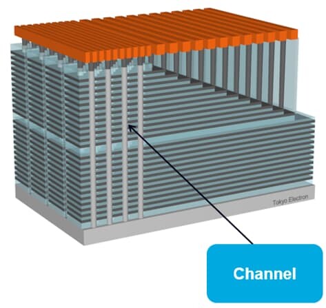
Tokyo Electron Develops Memory Channel Hole Etching for 400+ Layer 3D NAND Flash
Tokyo Electron announced that its development team at Tokyo Electron Miyagi—the development and manufacturing site for its plasma etch systems—has developed an innovative etch technology capable of producing memory channel holes in advanced 3D NAND devices with a stack of over 400 layers. The new process developed by the team has brought dielectric etch application to the cryogenic temperature range for the first time, producing a system with exceptionally high etch rates.
The innovative technology not only enables a 10-µm-deep etch with a high aspect ratio in just 33 minutes, but also can reduce the global warming potential by 84% compared with previous technologies. The geometry of the etched structure is quite well-defined as shown in the figure 1. Potential innovations enabled by this technology will spur creation of 3D NAND flash memory with even larger capacity.


The innovative technology not only enables a 10-µm-deep etch with a high aspect ratio in just 33 minutes, but also can reduce the global warming potential by 84% compared with previous technologies. The geometry of the etched structure is quite well-defined as shown in the figure 1. Potential innovations enabled by this technology will spur creation of 3D NAND flash memory with even larger capacity.

Mar 26th, 2025 08:58 EDT
change timezone
Latest GPU Drivers
New Forum Posts
- The TPU UK Clubhouse (25959)
- Packing Ties vs. Cable/Zip Ties (2)
- Should you physically remove secondary NVMe drives when performing a clean Windows install? (8)
- Windows 10 Vs 11, Which one too choose? (104)
- Discussion: linux-6.14.X (10)
- Recommended PhysX card for 5xxx series? [Is vRAM relevant?] (220)
- Is RX 9070 VRAM temperature regular value or hotspot? (208)
- any alternative to razer synapse to adjust mouse settings (5)
- What features do you want to see in a first person survival horror game? (40)
- HP Workstations Owners Club (377)
Popular Reviews
- Assassin's Creed Shadows Performance Benchmark Review - 30 GPUs Compared
- be quiet! Pure Rock Pro 3 Black Review
- ASUS ProArt X870E-Creator Wi-Fi Review
- ASRock Radeon RX 9070 XT Taichi OC Review - Excellent Cooling
- Pulsar Feinmann F01 Review
- Sapphire Radeon RX 9070 XT Nitro+ Review - Beating NVIDIA
- ASRock Phantom Gaming B860I Lightning Wi-Fi Review
- ASUS GeForce RTX 5070 TUF OC Review
- AMD Ryzen 9 9950X3D Review - Great for Gaming and Productivity
- AMD Ryzen 7 9800X3D Review - The Best Gaming Processor
Controversial News Posts
- AMD RDNA 4 and Radeon RX 9070 Series Unveiled: $549 & $599 (260)
- AMD Radeon RX 9070-series Pricing Leaks Courtesy of MicroCenter (158)
- MSI Doesn't Plan Radeon RX 9000 Series GPUs, Skips AMD RDNA 4 Generation Entirely (142)
- Microsoft Introduces Copilot for Gaming (123)
- AMD Radeon RX 9070 XT Reportedly Outperforms RTX 5080 Through Undervolting (118)
- NVIDIA Reportedly Prepares GeForce RTX 5060 and RTX 5060 Ti Unveil Tomorrow (115)
- Over 200,000 Sold Radeon RX 9070 and RX 9070 XT GPUs? AMD Says No Number was Given (100)
- NVIDIA GeForce RTX 5050, RTX 5060, and RTX 5060 Ti Specifications Leak (96)