News Posts matching #Yangtze Memory Technologies

Return to Keyword Browsing

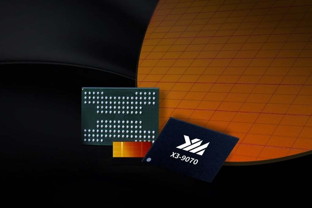
YMTC Starts Shipping 5th Generation NAND Flash with 294 Layers

Yangtze Memory Technologies Co. has begun shipping its fifth-generation 3D NAND memory chips, featuring 294 total layers and 232 active layers, according to an analysis from TechInsights. The new chips achieve bit density near 20 Gb per square millimeter (19.8 Gb/mm²), comparable to current offerings from SK Hynix and approaching Kioxia/Western Digital's latest products. YMTC's design uses hybrid bonding to connect the memory array with logic components, suggesting that Chinese memory makers are up to speed on the packaging standards that their non-sanctioned competitors use. The company has opted for a quiet release without formal announcements, a departure from typical industry practice. This low-key approach may be related to ongoing US trade restrictions on Chinese semiconductor companies.

While not setting records for active layers, SK Hynix's upcoming 321-layer chip leads in that metric, and YMTC's achievement in total layer count demonstrates continued technical progress. The chip uses string stacking technology, though the specific configuration of the layer arrays remains unclear. Other specifications show the new chip employs YMTC's Xtacking 4.0 architecture and triple-level cell (TLC) design. This matches major competitors' architecture type, though detailed performance metrics such as interface speeds have not been disclosed. The 5th generation NAND focuses on getting density on the right track. However, we expect YMTC to continue development at the same speed, match SK Hynix with 321-layer chips, and surpass it with Xtacking 5.0 in the near future.

China Launches Massive $47.5 Billion "Big Fund" to Boost Domestic Chip Industry

Beijing has doubled down on its push for semiconductor self-sufficiency with the establishment of a new $47.5 billion investment fund to accelerate growth in the domestic chip sector. The fund, officially registered on May 24th under the name "China Integrated Circuit Industry Investment Fund Phase III", represents the largest of three state-backed vehicles aimed at cultivating China's semiconductor capabilities. The announcement comes as tensions over advanced chip technology continue to escalate between the U.S. and China. Over the past couple years, Washington has steadily ratcheted up export controls on semiconductors to Beijing over national security concerns about potential military applications. These measures have lent new urgency to China's quest for self-sufficiency in chip design and manufacturing.

With a war chest of 344 billion yuan ($47.5 billion), the "Big Fund" dwarfs the combined capital of the first two semiconductor investment vehicles launched in 2014 and 2019. Officials have outlined a multipronged strategy targeting key bottlenecks, focusing on equipment for chip fabrication plants. The fund has bankrolled major projects such as flash memory maker Yangtze Memory Technologies and leading foundries like SMIC and Huahong. China's homegrown chip industry still needs to catch up to global leaders like Intel, Samsung, and TSMC. However, the immense scale of state-directed capital illustrates Beijing's unwavering commitment to developing a self-reliant supply chain for semiconductors—a technology viewed as indispensable for economic and military competitiveness. News of the "Big Fund" sent Chinese chip stocks surging over 3% on hopes of fresh financing tailwinds.

CXMT Starts 18.5 nm DRAM Production at Initial Capacity of 100,000 Wafers per Month, YMTC Steps up R&D Amid Obstacles

In a bold move to circumvent US sanctions imposed on Chinese chipmakers, ChangXin Memory Technologies (CXMT) and Yangtze Memory Technologies (YMTC), leading Chinese suppliers of DRAM and NAND flash memory respectively, are pursuing distinct strategies to accelerate development despite US export restrictions. Sources at DigiTimes indicate that CXMT has commenced mass production of 18.5 nm process DRAM chips at its new plant in Hefei. By slightly exceeding the US limit of 18 nm, CXMT aims to increase capacity while technically complying with Commerce Department rules. The phase-one Hefei plant is nearly at full utilization, with monthly output reaching 100,000 wafers. The upcoming phase-two expansion, adding 40,000 monthly wafers by the end of 2024, could give CXMT 10% of total DRAM capacity at global scale. Moreover, CXMT plans to increase domestic sourcing for the new expansion significantly.

In contrast, YMTC's capacity growth faces constraints across the board after being added to the US Entity List. With imports of key equipment now halted, building up local supply chains for materials and tools has proven challenging. Despite R&D advances, including NAND flash with over 300 layers, YMTC has introduced new 120-layer products that intentionally fall under the US limit of 128. However, even these compliant chips await US approval for higher production. Looking ahead, while CXMT has carved a viable path around US restrictions, YMTC's capacity plans face ongoing obstacles. Still, through determined R&D efforts, including 232-layer and future 300+ layer NAND, YMTC aims to push China's semiconductor capabilities forward despite external headwinds.
Return to Keyword Browsing
Feb 22nd, 2025 06:38 EST change timezone

New Forum Posts

Popular Reviews

Controversial News Posts