 95
95
AMD Radeon RX 5500 Review
Test Setup »High-resolution PCB Pictures
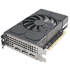
These pictures are for the convenience of volt modders and people who would like to see all the finer details on the PCB. Feel free to link back to us and use these in your articles or forum posts.High-res versions are also available (front, back).
Circuit Board (PCB) Analysis
The GPU VRM is a staggering 6-phase setup controlled by an International Rectifier IR35217 controller mated with LFPAK MOSFETs.
The memory VRM is single-phase and managed by an OnSemi NCP81022N controller (another premium part that's originally designed for 4 phases).
The GDDR6 memory chips are made by Samsung and carry the model number K4Z80325BC-HC14. They are specified to run at 1750 MHz (14 Gbps GDDR6 effective).
AMD's Navi 14 graphics processor is their second chip to use the new RDNA graphics architecture. It is made on a 7 nanometer silicon fabrication process at TSMC, and has a transistor-count of 6.4 billion. The die measures just 158 mm².
Mar 30th, 2025 23:43 EDT
change timezone
Latest GPU Drivers
New Forum Posts
- What do you do for a living? (446)
- Bluetooth to USB Conversion using a special circuit that I can create with my limited knowledge... (3)
- Will you buy a RTX 5090? (460)
- Alternatives to Autodesk Fusion 360 (4)
- Future-proofing my OLED (78)
- I'm looking for a good tool to make the 3D scanning of my mini-pc using the photogrammetry and my Kinect 2. (147)
- Question about Intel Optane SSDs (57)
- What is the latest game you finished or 100% (7)
- Is the futureproof gaming solution a four drive system? (23)
- Folding Pie and Milestones!! (9452)
Popular Reviews
- Sapphire Radeon RX 9070 XT Pulse Review
- ASRock Phantom Gaming B850 Riptide Wi-Fi Review - Amazing Price/Performance
- Samsung 9100 Pro 2 TB Review - The Best Gen 5 SSD
- Palit GeForce RTX 5070 GamingPro OC Review
- Sapphire Radeon RX 9070 XT Nitro+ Review - Beating NVIDIA
- Assassin's Creed Shadows Performance Benchmark Review - 30 GPUs Compared
- Enermax REVOLUTION D.F. 12 850 W Review
- AMD Ryzen 7 9800X3D Review - The Best Gaming Processor
- ASRock Radeon RX 9070 XT Taichi OC Review - Excellent Cooling
- XPG LEVANTE II 360 Review
Controversial News Posts
- AMD RDNA 4 and Radeon RX 9070 Series Unveiled: $549 & $599 (260)
- MSI Doesn't Plan Radeon RX 9000 Series GPUs, Skips AMD RDNA 4 Generation Entirely (142)
- Microsoft Introduces Copilot for Gaming (124)
- AMD Radeon RX 9070 XT Reportedly Outperforms RTX 5080 Through Undervolting (119)
- NVIDIA Reportedly Prepares GeForce RTX 5060 and RTX 5060 Ti Unveil Tomorrow (115)
- Over 200,000 Sold Radeon RX 9070 and RX 9070 XT GPUs? AMD Says No Number was Given (100)
- NVIDIA GeForce RTX 5050, RTX 5060, and RTX 5060 Ti Specifications Leak (96)
- Retailers Anticipate Increased Radeon RX 9070 Series Prices, After Initial Shipments of "MSRP" Models (90)


