 107
107
AMD Ryzen 5 7600 Review - Affordable Zen 4 for the Masses
(107 Comments) »Introduction
AMD today expanded its Ryzen 7000 "Zen 4" desktop processor lineup with three new affordable models that are designed to take the fight to Intel's expanded 13th Gen 65 W "Raptor Lake" series. In this review we take a closer look at the Ryzen 5 7600 6-core processor, the company's most affordable addition, which has the potential to become its most important one. Historically, Ryzen 5 non-X SKUs such as the 2600 and 3600, ended up being best-selling processors for AMD, as they struck incredible levels of value, competing very well with Intel's popular Core i5 65 W SKUs. With Zen 4, AMD is standardizing integrated graphics, and so a whole new market for AMD has opened up—businesses that buy 65 W Core i5 and Core i7 processors for their offices, and only need integrated graphics. The company's APUs from the past had been novelty products that compromised on CPU features in favor of strong iGPUs—not really something businesses need. With the new 65 W processors reviewed today, the company also includes a cooler in the box, which improves its value-proposition.

The new "Zen 4" microarchitecture and Socket AM5 platform modernize the processor for AMD. The new core introduces a 13% generational IPC uplift over "Zen 3," which when combined with boost frequencies in excess of 5 GHz enabled by the new 5 nm foundry node, improve single-threaded performance by as much as 29%. The new architecture also introduces several new instruction-sets, including support for AVX-512. The lowering of the TDP down to 65 W with 95 W package power tracking (PPT) should technically have no impact on single-threaded performance, or even performance for less-parallelized workloads, but could impact multi-threaded performance compared to the Ryzen 5 7600X, which enjoys 105 W TDP and 140 W PPT.
Unlike Intel, which really likes to segment their processors by taking away overclocking features, or limiting memory speeds, AMD doesn't do such a thing. All Ryzen 7000 non-X processors come with unlocked multipliers and even the mid-range B650 motherboard chipset offers CPU overclocking features.
The Ryzen 5 7600 is a 6-core/12-thread traditional multi-core processor. Each of its six cores is a high-performance core, comes with 1 MB of dedicated L2 cache, and 32 MB of on-die L3 cache is shared among the cores. The processor boosts up to 5.10 GHz, compared to 5.30 GHz of the 7600X. AMD is including a 65 W-capable Wraith Stealth stock cooling solution with the processor, and is pricing the 7600 at US $230, a price at which it squares off against several upcoming 65 W Core i5 "Raptor Lake" SKUs, such as the i5-13400 and i5-13500.
| Price | Cores / Threads | Base Clock | Max. Boost | L3 Cache | TDP | Architecture | Process | Socket | |
|---|---|---|---|---|---|---|---|---|---|
| Core i5-10400F | $115 | 6 / 12 | 2.9 GHz | 4.3 GHz | 12 MB | 65 W | Comet Lake | 14 nm | LGA 1200 |
| Core i5-11400F | $130 | 6 / 12 | 2.6 GHz | 4.4 GHz | 12 MB | 65 W | Rocket Lake | 14 nm | LGA 1200 |
| Core i5-12400F | $160 | 6 / 12 | 2.5 GHz | 4.4 GHz | 18 MB | 65 W | Alder Lake | 10 nm | LGA 1700 |
| Core i5-10500 | $230 | 6 / 12 | 3.1 GHz | 4.5 GHz | 12 MB | 65 W | Comet Lake | 14 nm | LGA 1200 |
| Ryzen 5 3600 | $135 | 6 / 12 | 3.6 GHz | 4.2 GHz | 32 MB | 65 W | Zen 2 | 7 nm | AM4 |
| Core i5-10600K | $220 | 6 / 12 | 4.1 GHz | 4.8 GHz | 12 MB | 125 W | Comet Lake | 14 nm | LGA 1200 |
| Core i5-11600K | $205 | 6 / 12 | 3.9 GHz | 4.9 GHz | 12 MB | 125 W | Rocket Lake | 14 nm | LGA 1200 |
| Ryzen 5 3600X | $195 | 6 / 12 | 3.8 GHz | 4.4 GHz | 32 MB | 95 W | Zen 2 | 7 nm | AM4 |
| Ryzen 5 5600 | $135 | 6 / 12 | 3.5 GHz | 4.4 GHz | 32 MB | 65 W | Zen 3 | 7 nm | AM4 |
| Ryzen 5 5600G | $130 | 6 / 12 | 3.9 GHz | 4.4 GHz | 16 MB | 65 W | Zen 3 + Vega | 7 nm | AM4 |
| Ryzen 5 5600X | $160 | 6 / 12 | 3.7 GHz | 4.6 GHz | 32 MB | 65 W | Zen 3 | 7 nm | AM4 |
| Core i5-12600 | $230 | 6 / 12 | 3.3 GHz | 4.8 GHz | 18 MB | 65 W | Alder Lake | 10 nm | LGA 1700 |
| Core i5-12600K | $250 | 6+4 / 16 | 3.7 / 2.8 GHz | 4.9 / 3.6 GHz | 20 MB | 125 W | Alder Lake | 10 nm | LGA 1700 |
| Core i5-13600K | $320 | 6+8 / 20 | 3.5 / 2.6 GHz | 5.1 / 3.9 GHz | 24 MB | 125 W | Raptor Lake | 10 nm | LGA 1700 |
| Core i7-10700K | $300 | 8 / 16 | 3.8 GHz | 5.1 GHz | 16 MB | 125 W | Comet Lake | 14 nm | LGA 1200 |
| Core i7-11700K | $280 | 8 / 16 | 3.6 GHz | 5.0 GHz | 16 MB | 125 W | Rocket Lake | 14 nm | LGA 1200 |
| Ryzen 7 3700X | $215 | 8 / 16 | 3.6 GHz | 4.4 GHz | 32 MB | 65 W | Zen 2 | 7 nm | AM4 |
| Ryzen 7 5700G | $180 | 8 / 16 | 3.8 GHz | 4.6 GHz | 16 MB | 65 W | Zen 3 + Vega | 7 nm | AM4 |
| Core i7-12700K | $325 | 8+4 / 20 | 3.6 / 2.7 GHz | 5.0 / 3.8 GHz | 25 MB | 125 W | Alder Lake | 10 nm | LGA 1700 |
| Ryzen 7 5700X | $200 | 8 / 16 | 3.4 GHz | 4.6 GHz | 32 MB | 65 W | Zen 3 | 7 nm | AM4 |
| Core i7-13700K | $430 | 8+8 / 24 | 3.4 / 2.5 GHz | 5.4 / 4.2 GHz | 30 MB | 125 W | Raptor Lake | 10 nm | LGA 1700 |
| Ryzen 7 5800X | $270 | 8 / 16 | 3.8 GHz | 4.7 GHz | 32 MB | 105 W | Zen 3 | 7 nm | AM4 |
| Ryzen 7 5800X3D | $360 | 8 / 16 | 3.4 GHz | 4.5 GHz | 96 MB | 105 W | Zen 3 | 7 nm | AM4 |
| Core i9-10900 | $355 | 10 / 20 | 2.8 GHz | 5.2 GHz | 20 MB | 65 W | Comet Lake | 14 nm | LGA 1200 |
| Ryzen 9 3900X | $380 | 12 / 24 | 3.8 GHz | 4.6 GHz | 64 MB | 105 W | Zen 2 | 7 nm | AM4 |
| Ryzen 5 7600 | $230 | 6 / 12 | 3.8 GHz | 5.1 GHz | 32 MB | 65 W | Zen 4 | 5 nm | AM5 |
| Ryzen 5 7600X | $300 | 6 / 12 | 4.7 GHz | 5.3 GHz | 32 MB | 105 W | Zen 4 | 5 nm | AM5 |
| Ryzen 9 5900X | $350 | 12 / 24 | 3.7 GHz | 4.8 GHz | 64 MB | 105 W | Zen 3 | 7 nm | AM4 |
| Core i9-10900K | $355 | 10 / 20 | 3.7 GHz | 5.3 GHz | 20 MB | 125 W | Comet Lake | 14 nm | LGA 1200 |
| Core i9-11900K | $350 | 8 / 16 | 3.5 GHz | 5.3 GHz | 16 MB | 125 W | Rocket Lake | 14 nm | LGA 1200 |
| Ryzen 9 3950X | $495 | 16 / 32 | 3.5 GHz | 4.7 GHz | 64 MB | 105 W | Zen 2 | 7 nm | AM4 |
| Ryzen 9 5950X | $600 | 16 / 32 | 3.4 GHz | 4.9 GHz | 64 MB | 105 W | Zen 3 | 7 nm | AM4 |
| Ryzen 7 7700 | $330 | 8 / 16 | 3.8 GHz | 5.3 GHz | 32 MB | 65 W | Zen 4 | 5 nm | AM5 |
| Ryzen 7 7700X | $345 | 8 / 16 | 4.5 GHz | 5.4 GHz | 32 MB | 105 W | Zen 4 | 5 nm | AM5 |
The Zen 4 Platform
AMD Zen has been one of the most remarkable turnarounds for a company in the semiconductor industry, and has had a profound impact on the consumer, as it influenced Intel's CPU core-counts. With each new generation of Zen, AMD delivered IPC and overall performance improvements, and Zen 4 stands out as it not only aims to improve performance, but also introduce a brand-new platform after five years of Socket AM4. As a parting gift, AMD enabled official Zen 3 support on even the oldest 300-series chipset, going to show just how consumer-friendly AM4 was, something the company hopes to repeat with AM5. The new AM5 socket was needed as the company enables the latest I/O, including DDR5 memory and PCI-Express Gen 5, besides power-delivery improvements. The socket can now deliver up to 230 W of power, which gives AMD room to increase CPU core-counts in the future. AM5 is a land-grid array, just like Intel desktop sockets, but the company somehow retained CPU cooler compatibility with AM4.
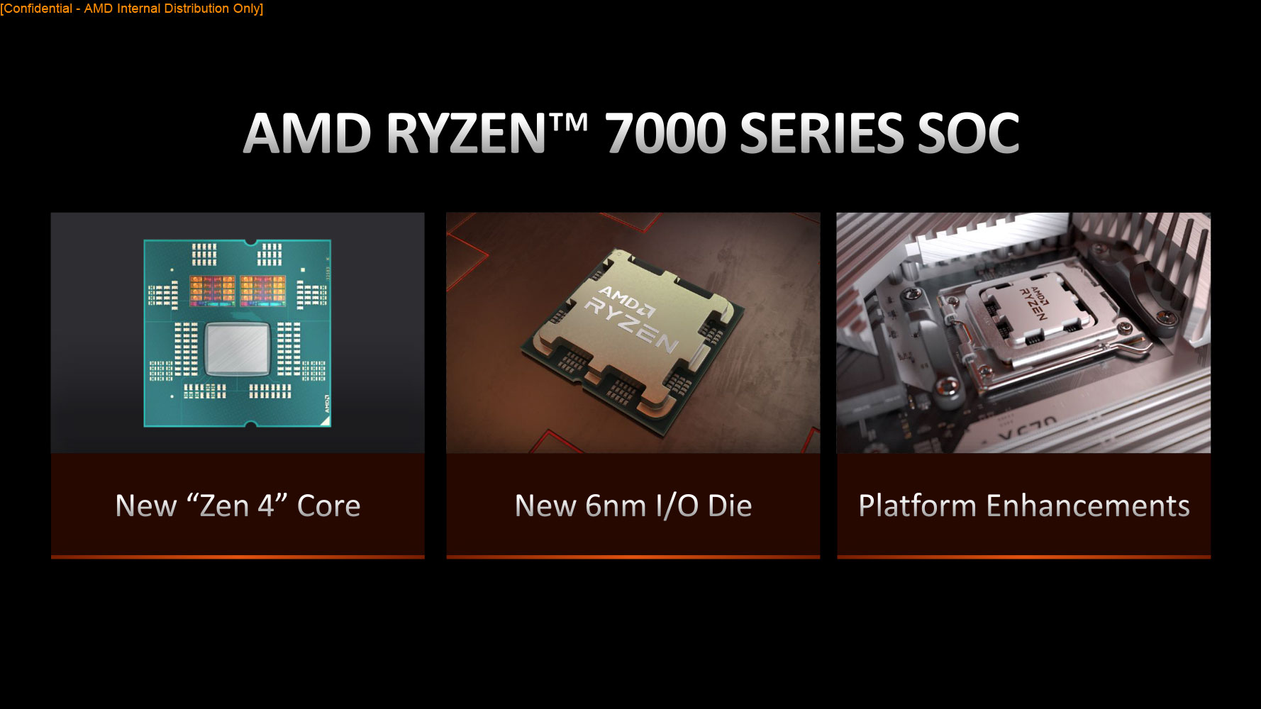
Zen 4 Chip Configuration


The Ryzen 7000 series desktop processor, codenamed "Raphael," is a multi-chip module, just like the Ryzen 5000 "Vermeer" and Ryzen 3000 "Matisse." The CPU cores are located in specialized dies called CCDs (CPU complex dies), while the platform I/O control is located in a separate die called cIOD (client I/O die). The CCDs were fabricated on the latest TSMC 5 nm EUV (N5) node, while the cIOD are done so on TSMC 6 nm (N6) nodes. The idea here is that the parts that benefit the most from the switch to the latest foundry process—the CPU cores—are built on this node; while everything else that can do with a slightly older node, is done so. This way AMD can make the most of its 5 nm foundry allocation with TSMC. The MCM contains a cIOD, and two 8-core CCDs in case of the Ryzen 9 7950X and 7900X; or one 8-core CCD in case of the Ryzen 7 7700X and Ryzen 5 7600X. Infinity Fabric interconnect handles communications not just within these dies, but also between them. The transition to fast DDR5 memory and PCIe Gen 5 means that AMD now can push instructions and data around faster. It did so with microarchitectural improvements to the "Zen 4" core itself, while increasing the Infinity Fabric bandwidth between the cores.
The Zen 4 CPU Core
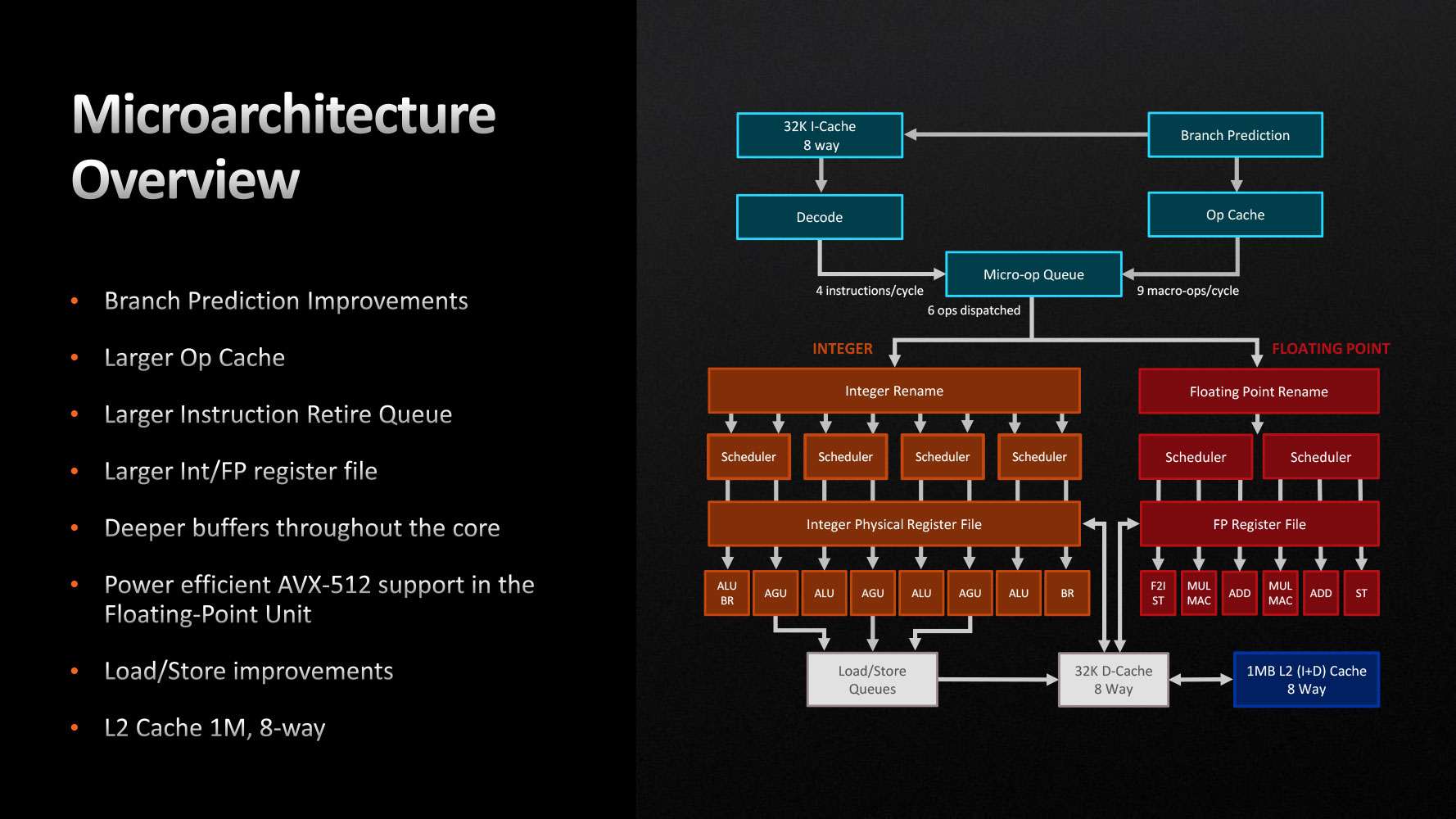

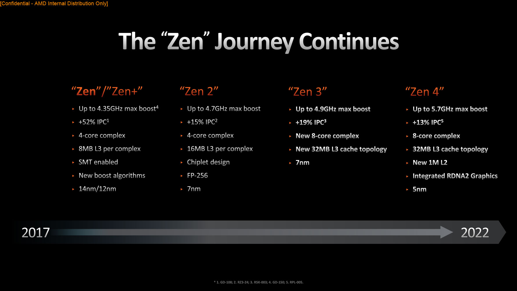
All cores in Ryzen 7000 series processors are of the same kind, or what Intel would consider a performance-core, or P-core. AMD has worked on all three key stages of the CPU—the front-end, the execution, and the load/store. The front-end is the "mouth" of the CPU core, and prepares data and instructions for execution. Front-end improvements begin at the Branch Prediction unit, which can how predict 2 taken branches per clock-cycle, and comes with larger L1 and L2 branch-target buffers (BTBs). AMD had for the very first time introduced an OpCache with Zen, improving it over time. AMD has increased the size of the OpCache by around 68 percent. It can now handle 9 macro-ops per cycle. The micro-op queue dispatch rate to the execution stage is still 6.

The Execution Stage is the main number-crunching machinery, and broadly features two components for the kind of math workload being executed—Integer and Floating Point. The "Zen 4" execution stage features a 25% larger instruction retire queue, larger register files, and higher buffer queue-depths throughout the core.
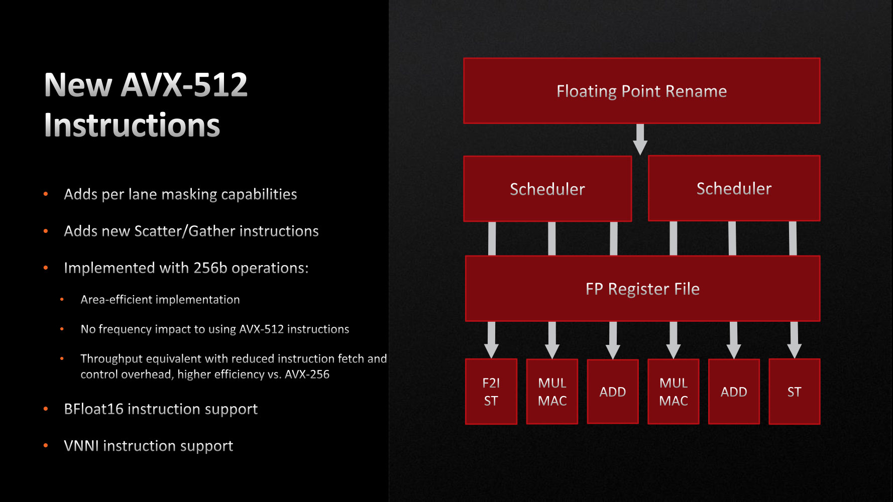

With "Zen 4," AMD is introducing support for AVX-512, in a bid to increase the processor's AI inferencing performance. The company did this in a die-area efficient, and energy-efficient manner, with no impact on CPU core frequency. AVX-512 operations are executed on a dual-pumped 256-bit FPU, rather than building ground-up 512-bit FP machinery. VNNI and Bfloat16 instruction-sets are also added, which mean that "Zen 4" can handle pretty much all of the AVX-512 client-relevant workloads that competing Intel processors can.


The Load/Store unit is the part of the core that interfaces with the memory sub-system. The "Zen 4" core gets a 22 percent larger Load Queue, with improved data-port conflict-resolution. There's a 50% larger L2 data transition lookaside buffer. The cache-hierarchy of the Ryzen 7000 desktop processor is similar to that of Ryzen 5000, with a few key differences, besides bandwidth/latency improvements—the dedicated L2 cache has been doubled in size to 1 MB. The eight CPU cores on a CCD share a monolithic 32 MB L3 cache, with uniform access to each core.

These improvements contribute to a 13 percent IPC improvement over "Zen 3," AMD claims. The company provided a break-up of which components are contributing to the IPC uplift, and we see that close to two-thirds of it are coming from improvements to the front-end and load/store stages. Branch prediction improvements contribute a fifth of this uplift. Interestingly, the L2 cache contributes barely 1/10th of the IPC uplift, in the tested applications—we believe this increase is mostly relevant for server applications where it should be able to make a difference. Intel's "Golden Cove" P-core comes with 1.25 MB L2 cache, and the upcoming "Raptor Cove" is expected to feature 2 MB. Despite the doubling in L2 cache sizes, the resulting increase in cache latency is very well contained (from 12 cycles on the 512 KB L2 of "Zen 3," to just 14 cycles on "Zen 4").

VBS (virtualization-based security) is the standard on new Windows 11 installs and gets activated automatically, unless you specifically disable it. Windows 11 Security Center already flags VBS not being enabled as a warning, similar to Antivirus being disabled or outdated. AMD made several improvements to the Virtualization feature-set, to reduce its performance impact in a VBS-enabled client environment. This includes speculation control, dual AVIC to go with the physical dual-APIC, and TSC_AUX virtualization.
New 6 nm IO Die

Ryzen 3000 "Matisse" and Ryzen 5000 "Vermeer" processors featured a cIOD built on the 12 nm FinFET Global Foundries node, but with Ryzen 7000 "Raphael," AMD is taking a giant leap toward improving the power characteristics of the cIOD, by building it on the new 6 nm TSMC node. This was needed mainly because the cIOD now packs an RDNA 2 iGPU, besides the higher bandwidth switching fabric of the DDR5 and PCIe Gen 5 interfaces also warranting the change. The 12 nm previous-gen cIOD TDP was already estimated to be up to 15 W, and the addition of an iGPU would've thrown things off gear. In addition to 6 nm, AMD is deploying several of the power-management features of the Ryzen 6000-series "Rembrandt" mobile processor on this cIOD, which mainly have to do with aggressive power management and rapid sleep/wake for the various components on the die.
The new 6 nm cIOD packs a dual-channel DDR5 memory controller (4x 40-bit channels, including ECC and hardware-accelerated encryption support), with native support for DDR5-5200; a PCI-Express 5.0 x28 root-complex; a USB 3.2 controller with support for 20 Gbps 2x2 ports, USB-C, and DisplayPort passthrough from the iGPU. AMD was very clear that the inclusion of an iGPU doesn't make "Raphael" an APU, because the iGPU is rather basic, and just about enough for non-gaming workloads. The company intends to continue making APUs—processors with beefy iGPUs for mainstream gaming performance—including for the desktop platform. Full ECC support on desktop is technically possible, but it will depend on the motherboard manufacturers—AMD isn't doing anything to prevent them from making their boards ECC compatible.

The Radeon 610 iGPU is based on the RDNA 2 graphics architecture, and packs just two Compute Units, which work out to 128 stream processors. The Display CoreNext (DCN) and Video CoreNext (VCN) components are of modern design. The VCN offers hardware-accelerated AV1 and H.265 decode, as well as hardware-accelerated H.265 encode. Just to clarify, there is hardware AV1 decode support, but no encode, which isn't a big deal at all. In terms of monitors, the DCN supports DisplayPort 2.0 UHBR10, HDMI 2.1 with FRL, and DisplayPort passthrough for the USB type-C ports connected to the on-die USB 3.2 controller. When paired with a discrete graphics card on Windows 10 or Windows 11, the iGPU supports Hybrid graphics, much in the same way as it's implemented on notebooks. You plug in your monitor to the iGPU, and it wakes up your discrete GPU (graphics card) when needed. The RDNA 2 compute units are of the same kind you'd find in Radeon RX 6000 series GPUs, including ray tracing support, but this is of no use on the Radeon 610. The only reason AMD went with RDNA 2 is because it can offer comparable levels of performance with just two CUs, to a "Vega" based iGPU that would need more CUs (thereby increasing die-size).
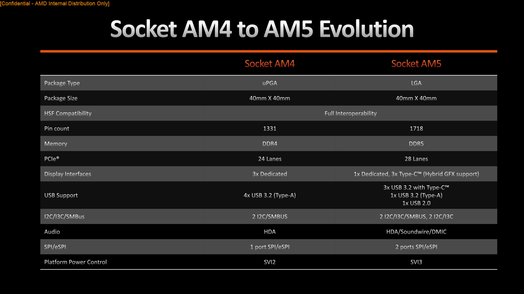

As we mentioned earlier, AMD needed a new socket as it was transitioning to DDR5 and PCIe Gen 5, which come with stiff physical-layer signaling requirements that AM4 couldn't provide. AM5 also makes processors "future-ready" as it enables two-way communication with the voltage regulators. The added pin-count was needed not just for DDR5 and its 40-bit sub-channels, but also for four additional PCIe lanes. The processor puts out a total of 28 PCIe Gen 5 lanes. 16 of these are meant for PEG (graphics card slots); 4 serve as chipset bus, and 8 lanes are available for the motherboard vendors to play around with: either wiring them both out as M.2 Gen 5 x4 slots, or wire one of them as M.2, and use the remaining 4 lanes for high-bandwidth devices, such as discrete USB4 controllers, 80 Gbps Thunderbolt 4 controllers, or even CPU-attached low-latency network interfaces. AM5 also significantly increases power-delivery capability over AM4—up to 230 W. The increased power should enable the "Zen 4" cores to run at very high clock-speeds approaching the 6 GHz-mark, or in the future, even enable core-count increases.

The clock-domains of Ryzen 7000 are similar to those of the Ryzen 5000 series. FCLK defines the Infinity Fabric clock-speed, which is de-linked from UCLK (memory controller clock), and MCLK (DRAM clock). AMD says that DDR5-6000 strikes the "sweetspot" in that this is the highest MCLK you can run while retaining certain memory overclocker optimizations. On Zen 3 you'd want to run Infinity Fabric in sync with memory, but this isn't possible anymore, because FCLK can't reach 3000 MHz (assuming DDR5-6000 memory). Now the optimum config is to run FCLK at 2000, basically a 3:2 divider. Picking "auto" in the BIOS will automatically aim for that setting. Above 6000 MHz, the strategy will be changed to 2:1 ratio.
AMD X670E and B650E Chipsets


AMD took a unique approach to chipsets with this generation. The top-tier chipset now comes in two flavors, X670E and X670. Both are identical in downstream I/O, but the X670E offers PCIe Gen 5 PEG besides CPU-attached Gen 5 NVMe; whereas the X670 only offers Gen 5 on the CPU-attached M.2 NVMe slot, but not PEG (which is Gen 4). A similar approach is taken when segregating the mid-tier B650E from the B650. The lack of Gen 5 PEG should significantly reduce motherboard costs, as designers would be saving on both Gen 5 redrivers and the steep wiring requirements to avoid signal-corruption.
X670E is a 2-chip chipset unlike the previous-gen X570. This was done to increase the downstream PCIe connectivity. The chipset now offers up to 12x PCIe Gen 4 and up to 8x PCIe Gen 3 downstream lanes (not counting the lanes from the CPU). This lets motherboard designers wire out three additional M.2 Gen 4 slots attached to the chipset, while the Gen 3 lanes handle low-bandwidth onboard devices. AMD adopted a wacky way to connect the two bridges that make up the chipset. There is an "upstream" chipset that's wired to the AM5 SoC over a PCI-Express 4.0 x4 connection; the second bridge is called "downstream" chipset, and is connected to four of the PCIe Gen 4 downstream lanes of the "upstream" chipset. The X670/E puts out up to two 20 Gbps USB 3.2, up to eight 10 Gbps USB 3.2, and twelve USB 2.0. The B650E and B650 look like more reasonable single-chip chipsets. They talk to the SoC over PCI-Express 4.0 x4, and wire out 8x PCIe Gen 4 downstream lanes, and up to 4x PCIe Gen 3 downstream lanes. You get half the number of USB SuperSpeed ports as the X670/E.
AMD EXPO Memory
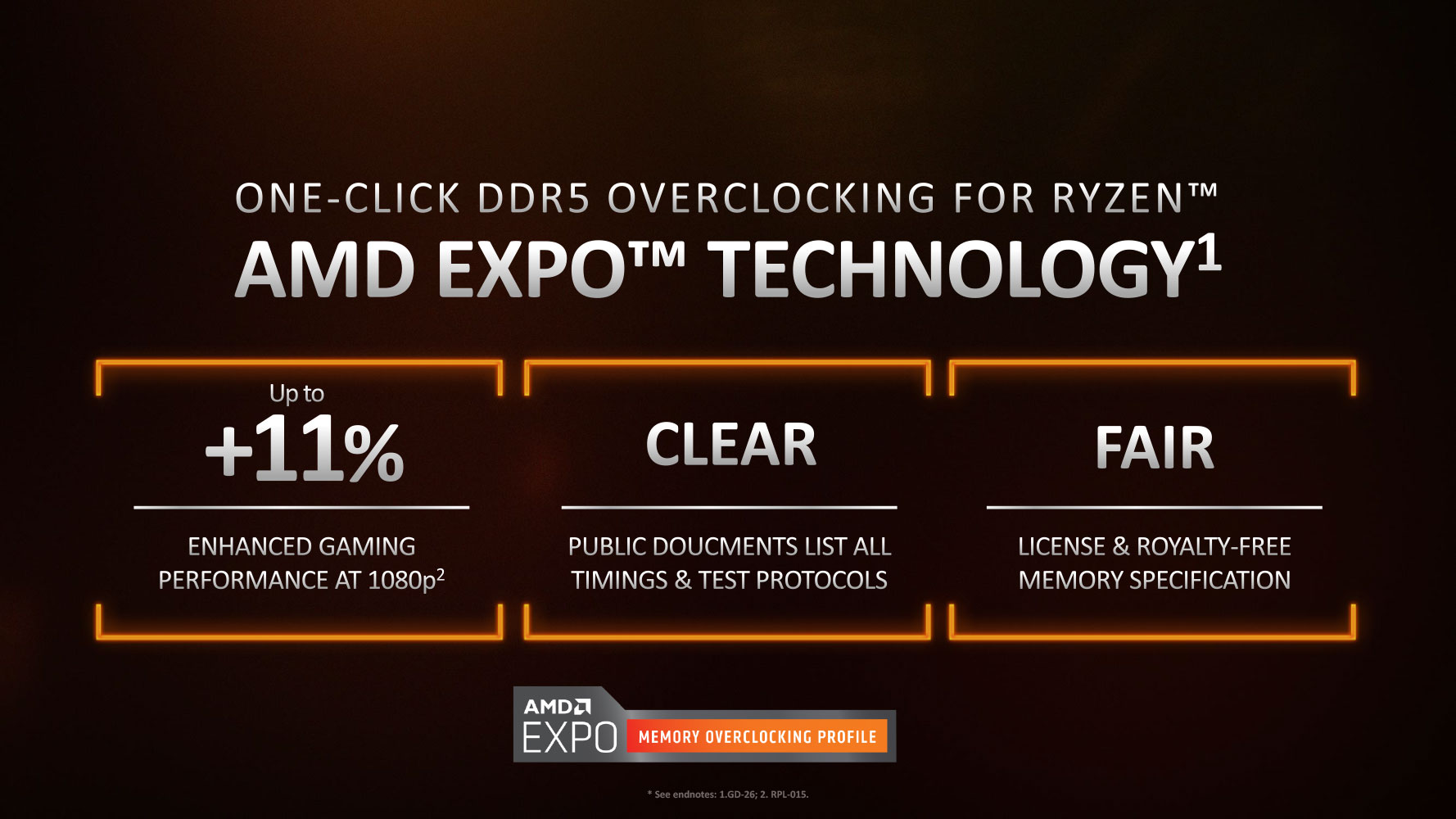
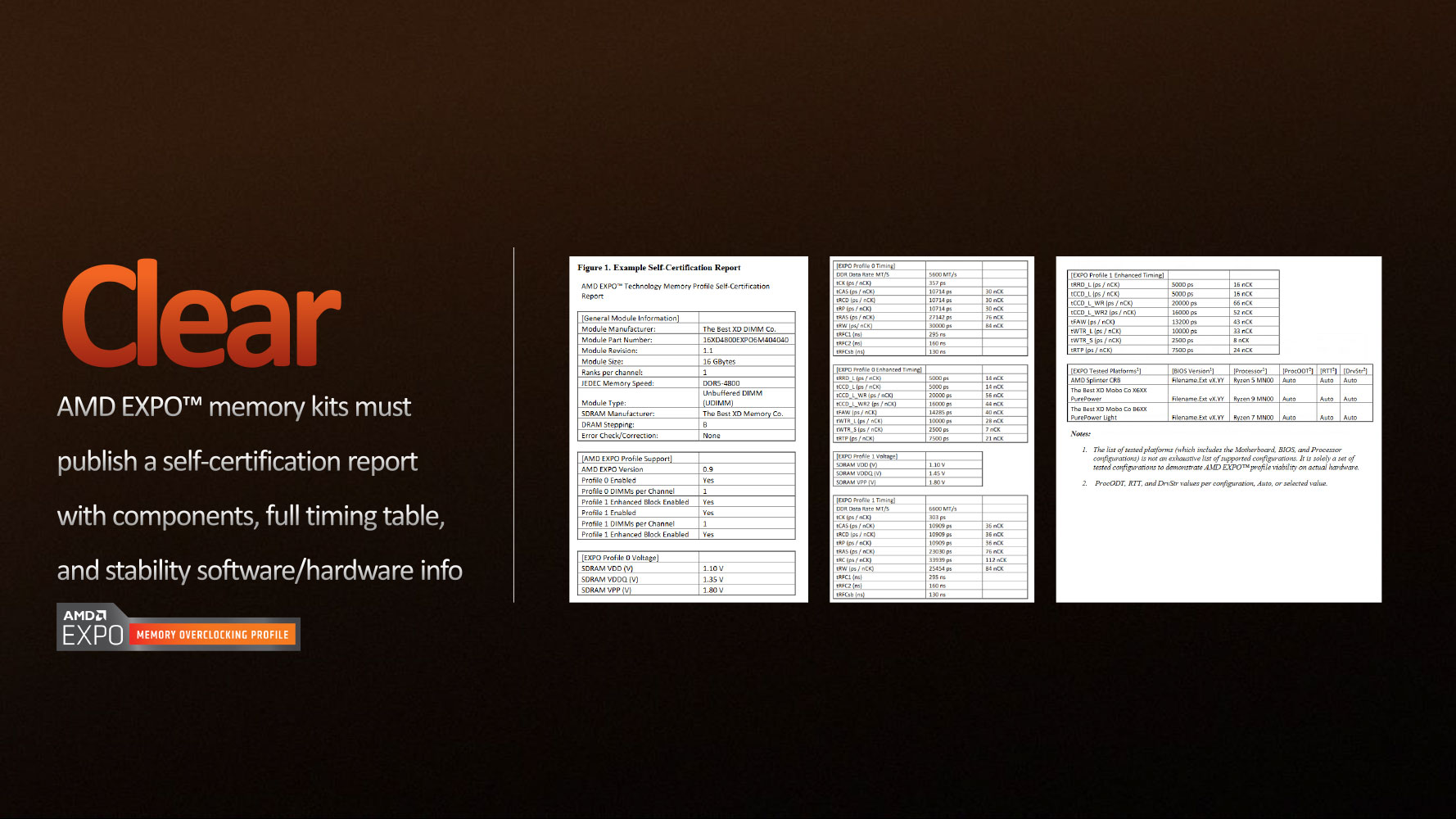
With Ryzen 7000 series, AMD is introducing EXPO (extended profiles for overclocking); a feature that's identical in concept to Intel XMP. AMD EXPO-certified DDR5 modules come with an easy method of applying the advertised memory speeds and timings—you simply select a toggle in the opening screen of your motherboard's UEFI BIOS program. EXPO differs from XMP in that it includes fine settings that are unique to the AMD architecture, and it's also an open standard. Until now, XMP modules installed on AMD systems relied either on painstaking manual overclocking, or use of DOCP, a feature that attempts to translate the settings in the XMP profile to "nearest neighbors" of AMD-compatible settings. This was sub-optimal. EXPO is royalty-free compared to XMP, so any memory manufacturer can implement it for free. Ryzen 7000 can run any PC-DDR5 memory in the market, including XMP-certified ones, so don't fret if you can't find EXPO kits just yet.
Our Patreon Silver Supporters can read articles in single-page format.
Mar 30th, 2025 23:13 EDT
change timezone
Latest GPU Drivers
New Forum Posts
- What do you do for a living? (444)
- Will you buy a RTX 5090? (459)
- Alternatives to Autodesk Fusion 360 (4)
- Future-proofing my OLED (78)
- I'm looking for a good tool to make the 3D scanning of my mini-pc using the photogrammetry and my Kinect 2. (147)
- Question about Intel Optane SSDs (57)
- What is the latest game you finished or 100% (7)
- Is the futureproof gaming solution a four drive system? (23)
- Folding Pie and Milestones!! (9452)
- Looking for Palit 5090 Gamerock OC BIOS (19)
Popular Reviews
- Sapphire Radeon RX 9070 XT Pulse Review
- ASRock Phantom Gaming B850 Riptide Wi-Fi Review - Amazing Price/Performance
- Samsung 9100 Pro 2 TB Review - The Best Gen 5 SSD
- Palit GeForce RTX 5070 GamingPro OC Review
- Sapphire Radeon RX 9070 XT Nitro+ Review - Beating NVIDIA
- Assassin's Creed Shadows Performance Benchmark Review - 30 GPUs Compared
- Enermax REVOLUTION D.F. 12 850 W Review
- AMD Ryzen 7 9800X3D Review - The Best Gaming Processor
- ASRock Radeon RX 9070 XT Taichi OC Review - Excellent Cooling
- XPG LEVANTE II 360 Review
Controversial News Posts
- AMD RDNA 4 and Radeon RX 9070 Series Unveiled: $549 & $599 (260)
- MSI Doesn't Plan Radeon RX 9000 Series GPUs, Skips AMD RDNA 4 Generation Entirely (142)
- Microsoft Introduces Copilot for Gaming (124)
- AMD Radeon RX 9070 XT Reportedly Outperforms RTX 5080 Through Undervolting (119)
- NVIDIA Reportedly Prepares GeForce RTX 5060 and RTX 5060 Ti Unveil Tomorrow (115)
- Over 200,000 Sold Radeon RX 9070 and RX 9070 XT GPUs? AMD Says No Number was Given (100)
- NVIDIA GeForce RTX 5050, RTX 5060, and RTX 5060 Ti Specifications Leak (96)
- Retailers Anticipate Increased Radeon RX 9070 Series Prices, After Initial Shipments of "MSRP" Models (90)