 73
73
AMD Ryzen 9 3900XT Review
(73 Comments) »Introduction
AMD today released the new Ryzen XT Family, and here's our Ryzen 9 3900XT review. These processors are being launched by AMD as its first response to Intel's 10th Gen Core "Comet Lake" processor family and are based on the "Zen 2" microarchitecture, which established a technological superiority over Intel and tilted the DIY retail channel market leadership firmly over to AMD. Just a year ago, "Zen 2" introduced many firsts, including the new 7 nm silicon fabrication process, PCI-Express 4.0, and core counts of up to 16 on the existing AM4 mainstream desktop socket, with backwards compatibility with older 400-series chipsets.
AMD has been largely unopposed by Intel since July 2019. Much of AMD's leadership rests on the fact that "Zen 2" matches the IPC of the "Skylake" CPU core, and AMD is able to offer more cores or threads to the dollar than Intel. In response, Intel's strategy with "Comet Lake" has been to open up the "Skylake" core across the board by enabling HyperThreading for the entire Core i3, Core i5, Core i7, and Core i9 brands, and increasing L3 cache. Intel didn't stop there. In addition to stepping up clock speeds, Intel introduced new boosting algorithms for its Core i7 and Core i9 chips, including Turbo Boost Max 3.0 and Thermal Velocity Boost and significantly bumped power limits (up to 125 W). The company also gave motherboard designers freedom to play with power limits and offer them as user-configurable BIOS settings.

The Core i9-10900K has hence spelled trouble for the Ryzen 9 3900X. In our testing, it beat the AMD chip by 2% in CPU tests despite two fewer cores, and it is some 7% ahead in gaming performance because of its higher frequencies. This forced AMD to get retailers to unofficially cut prices of the 3900X down to $420, leaving a vast price-performance gorge between it and the flagship Ryzen 9 3950X. AMD needs something to sell at $499 again, or it cedes that price-segment to the i9-10900K. We hence have the Ryzen 9 3900XT.
Launched today at $499, the Ryzen 9 3900XT is a 12-core/24-thread Socket AM4 processor that's drop-in compatible with any motherboard that supports Ryzen 3000 series processors. The processor ships with clock speeds of 3.80 GHz base, same as the 3900X, but increased 4.70 GHz boost frequency, compared to the 4.60 GHz of the 3900X. There's more to this 100 MHz increment. AMD built these processors on a refinement of TSMC's N7 (7 nm) silicon fabrication node, which helps with improved boost frequency sustainability and has AMD claim performance gains in both single and multi-threaded tasks. More on this later.
A design focus with the Ryzen 3000XT series has been to shore up gaming performance since the original Ryzen 3000 chips didn't end up too far behind Intel's 10th Gen Core chips. AMD neither wants to lose competitive price points nor the gaming performance outlook to Intel for the next months, while they give finishing touches to the "Zen 3" microarchitecture.
An interesting product design decision by AMD has been to drop the in-box cooling solution with the Ryzen 9 3900XT. Unlike the 3900X, which includes an AMD Wraith Prism RGB cooler, the Ryzen 9 3900XT lacks a cooler. AMD claims that a majority of the audience for the 3900X uses aftermarket cooling, or even watercooling. The more obvious explanation has to do with cost cutting since this could be a straight $25–$30 saving for the company per box. Intel doesn't include coolers with its unlocked K-series processors, either.
In our Ryzen 9 3900XT review we put AMD's new CPU through our entire CPU test suite and compare it with all interesting models from Intel's Comet Lake lineup, as well as the Ryzen 9 3900X.
| Price | Cores / Threads | Base Clock | Max. Boost | L3 Cache | TDP | Architecture | Process | Socket | |
|---|---|---|---|---|---|---|---|---|---|
| Core i5-10600K | $265 | 6 / 12 | 4.1 GHz | 4.8 GHz | 12 MB | 125 W | Comet Lake | 14 nm | LGA 1200 |
| Ryzen 5 3600X | $205 | 6 / 12 | 3.8 GHz | 4.4 GHz | 32 MB | 95 W | Zen 2 | 7 nm | AM4 |
| Ryzen 5 3600XT | $250 | 6 / 12 | 3.8 GHz | 4.5 GHz | 32 MB | 95 W | Zen 2 | 7 nm | AM4 |
| Ryzen 7 1800X | $250 | 8 / 16 | 3.6 GHz | 4.0 GHz | 16 MB | 95 W | Zen | 14 nm | AM4 |
| Core i7-8700K | $350 | 6 / 12 | 3.7 GHz | 4.7 GHz | 12 MB | 95 W | Coffee Lake | 14 nm | LGA 1151 |
| Core i7-9700K | $380 | 8 / 8 | 3.6 GHz | 4.9 GHz | 12 MB | 95 W | Coffee Lake | 14 nm | LGA 1151 |
| Core i7-10700K | $375 | 8 / 16 | 3.8 GHz | 5.1 GHz | 16 MB | 125 W | Comet Lake | 14 nm | LGA 1200 |
| Ryzen 7 3700X | $275 | 8 / 16 | 3.6 GHz | 4.4 GHz | 32 MB | 65 W | Zen 2 | 7 nm | AM4 |
| Ryzen 7 3800X | $340 | 8 / 16 | 3.9 GHz | 4.5 GHz | 32 MB | 105 W | Zen 2 | 7 nm | AM4 |
| Ryzen 7 3800XT | $400 | 8 / 16 | 3.9 GHz | 4.7 GHz | 32 MB | 105 W | Zen 2 | 7 nm | AM4 |
| Ryzen 9 3900X | $430 | 12 / 24 | 3.8 GHz | 4.6 GHz | 64 MB | 105 W | Zen 2 | 7 nm | AM4 |
| Ryzen 9 3900XT | $500 | 12 / 24 | 3.8 GHz | 4.7 GHz | 64 MB | 105 W | Zen 2 | 7 nm | AM4 |
| Core i9-9900K | $530 | 8 / 16 | 3.6 GHz | 5.0 GHz | 16 MB | 95 W | Coffee Lake | 14 nm | LGA 1151 |
| Core i9-9900KS | $600 | 8 / 16 | 4.0 GHz | 5.0 GHz | 16 MB | 127 W | Coffee Lake | 14 nm | LGA 1151 |
| Core i9-10900K | $500 | 10 / 20 | 3.7 GHz | 5.3 GHz | 20 MB | 125 W | Comet Lake | 14 nm | LGA 1200 |
| Ryzen 9 3950X | $720 | 16 / 32 | 3.5 GHz | 4.7 GHz | 72 MB | 105 W | Zen 2 | 7 nm | AM4 |
A Closer Look


AMD Ryzen 9 3900XT ships in an upscale-looking paperboard box with a cutout showing the processor inside, which is identical-looking to the one the flagship Ryzen 9 3950X comes in. The box does not include a cooler inside.


The processor looks like any conventional AMD CPU with a large IHS dominating the top, and a 1,331-pin micro-PGA in the bottom. The "Zen 2" CCD chiplet is made in Taiwan and the I/O die in the US, and the two are put together at a facility in China.
All Ryzen 3000XT series processors are designed to be drop-in compatible with any Socket AM4 motherboard that supports Ryzen 3000 processors.

Ryzen 9 3900XT can be paired with a fairly big selection of AM4-compatible coolers that have been released since 2017.
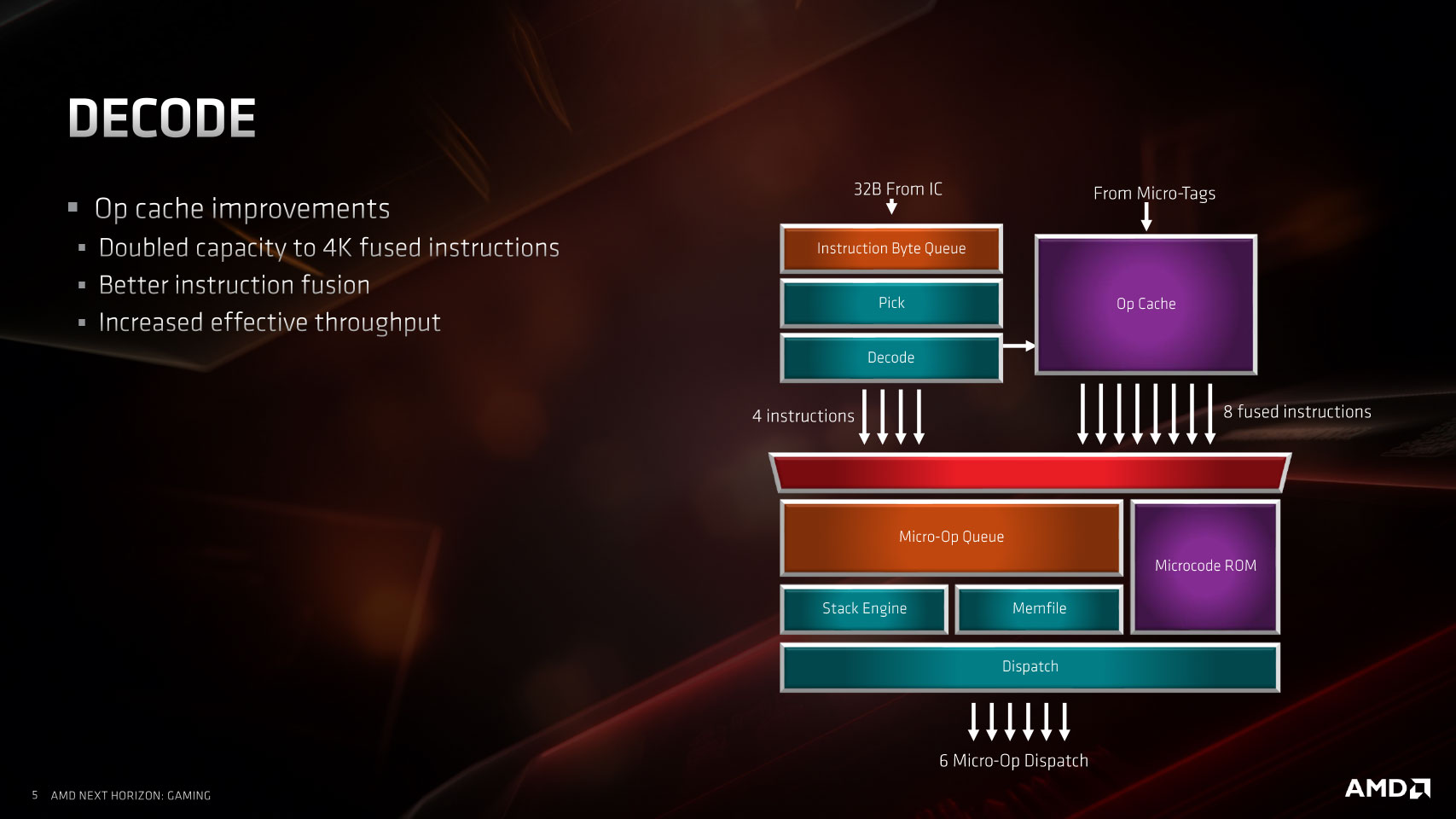
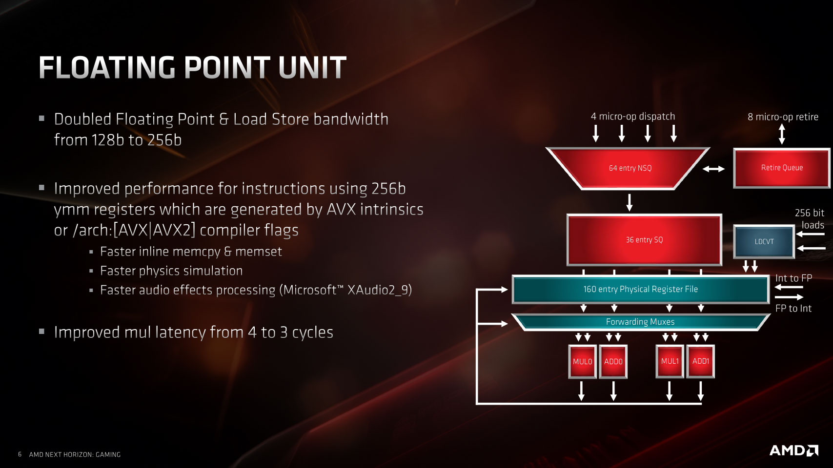
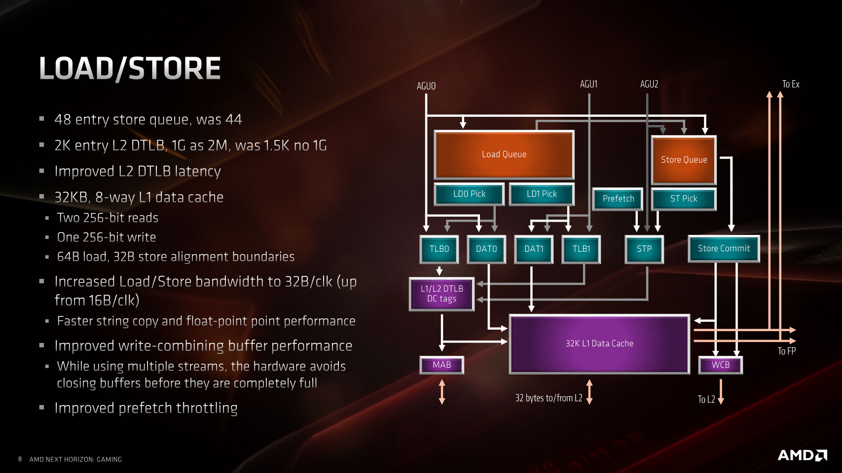
Architecture
The architecture is no different from the Ryzen 9 3950X or any other "Matisse," so you can click on the button below to read about it, or skip that section if you're familiar with it.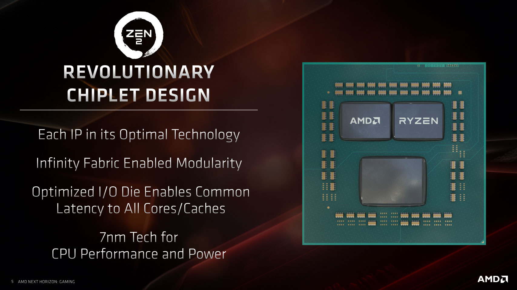


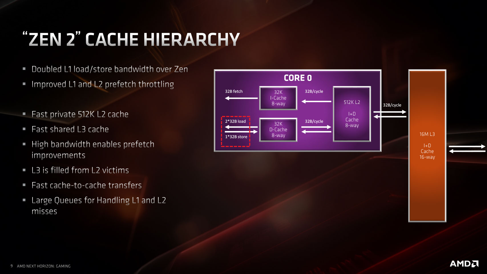


Architectural Innovations Specific to Ryzen 3000XT Series
The Ryzen 3000XT family of processors are internally referred by AMD as "Matisse 2." These are almost identical to the original Ryzen 3000 "Matisse" processors based on the "Zen 2" microarchitecture, but AMD has given these processors some physical improvements. To begin with, the 8-core CCDs (compute complex dies) or "Zen 2" chiplets inside the processors are still based on TSMC N7 (the foundry's first 7 nm node), but with certain refinements. AMD claims these yields a single-digit percentage electrical improvement, which AMD used to achieve up to 200 MHz increments in maximum boost frequencies without affecting the TDP of these processors.
The TDP of Ryzen 5 3600XT remains at 95 W, just like the 3600X, while the 3800XT and 3900XT both stick with 105 W TDP. AMD's decision not to include cooling solutions with the 3800XT and 3900XT have little to do with the power or thermals of these processors and more with marketing decisions. It certainly reduces AMD's bill of materials for these chips.
AMD categorically stated that this "refined" N7 node is neither N7P nor N7+. The N7P node is the successor to N7 that sticks to DUV (deep ultraviolet) lithography, but innovates in certain other areas to eke out a power improvement. N7+, on the other hand, uses EUV (extreme ultraviolet) lithography that not only yields a much higher efficiency, but also over a 20% increase in transistor density. The node AMD is building "Matisse 2" on is still N7, but with certain refinements AMD didn't elaborate in its product brief.
AMD B550 and X570 Chipsets
With premium AMD X570 chipset-based motherboards starting at $150, it's less likely that someone would pair the third-generation Ryzen 3 with it. Choosing a cheaper B450 motherboard would mean giving up on killer features such as PCIe gen 4.0. AMD hence launched the new B550 mid-range chipset. The B550 chipset lets you have PCI-Express gen 4.0 connectivity from the "Matisse" processor, while limiting general purpose PCIe downstream connectivity to gen 3.0.
On a typical B550 chipset motherboard, the main PCI-Express x16 slot will be gen 4.0 if paired with a third-generation Ryzen "Matisse" processor, as would one of the board's M.2 NVMe slots that's wired to the processor. All other PCIe or M.2 slots which are wired to the B550 chipset will be gen 3.0. This way, future-proofing of the platform for next-generation graphics cards and SSDs remains intact. The B550 chipset provides up to six SATA 6 Gbps ports with AHCI and RAID capability, up to two 10 Gbps USB 3.1 gen 2 ports (in addition to four such ports put out by the "Matisse" processor), two additional USB 3.1 gen 1 ports, and six USB 2.0 ports. The platform's HDA and LPCIO buses are located on the processor.
A word on compatibility. The B550 chipset only supports third-generation Ryzen "Matisse" processors as of this writing, and AMD confirmed support for next-generation processors based on the "Zen 3" architecture. You cannot pair a B550 motherboard with older Ryzen 2000/1000 processors or even the 3200G or 3400G APUs based on the older "Zen+" microarchitecture. There will be clear labeling on B550 chipset motherboard boxes to this effect.
What we like most about the B550 is its low TDP, which lets motherboard designers make do with passive heatsinks; unlike X570, which requires active fan heatsinks.

AMD delivered on its promise of third-generation Ryzen "Matisse" processors being backwards compatible with older Socket AM4 motherboards, going all the way back to the AMD 300-series chipset, with a simple BIOS update. To make the most out of Ryzen "Matisse"—namely, PCI-Express gen 4.0 connectivity and increased CPU/memory overclocking headroom, you're expected to use one of the latest motherboards that use the AMD X570 chipset. The X570 is an entirely different chip from X470 and X370. The older chipsets were supplied by ASMedia, and were rather slim in their downstream connectivity.
The X470 only puts out 8 PCIe gen 2.0 downstream lanes, for example. The X570 modernizes all I/O by putting out up to 16 PCIe gen 4.0 downstream lanes. This enables additional M.2 PCIe gen 4 slots on your motherboards for the latest SSDs featuring PCIe gen 4 support and creates room for many new bandwidth-hungry onboard devices, such as 10 GbE adapters, next-generation Thunderbolt, 802.11ax controllers, etc. Along with the "Matisse" SoC, the X570 also puts out a number of 10 Gbps USB 3.1 gen 2 ports. Motherboards based on X570 also implement modern network connectivity options, such as 2.5 GbE and 802.11ax WLAN.
Given there are highly capable motherboards based on the B550 chipset with serious VRM solutions and high-end connectivity, it's good enough for any Ryzen 3000XT series processor, including the 3900XT. The B550 chipset also offers multi-GPU support. Your choice between the B550 and X570 should hence boil down to whether you plan to have more than one M.2 NVMe SSD that can take advantage of PCI-Express gen 4.0, or an NVMe RAID setup of 2–3 PCIe gen 4.0-capable M.2 SSDs. Serious overclockers should still consider the X570 since the most beastly VRM setups are still found on boards such as the MSI MEG X570 GODLIKE, ASUS ROG Crosshair VII Formula, and GIGABYTE X570 AORUS Xtreme.
Our Patreon Silver Supporters can read articles in single-page format.
Mar 29th, 2025 06:56 EDT
change timezone
Latest GPU Drivers
New Forum Posts
- WCG Daily Numbers (12814)
- What are you playing? (23302)
- TPU's Rosetta Milestones and Daily Pie Thread (2259)
- Folding Pie and Milestones!! (9450)
- Someone run games on AMD BC-250 under Linux * Cut down PS5 die to 6 CPU cores 24 GPU cores for use in crypto mining (78)
- Upgrade from a AMD AM3+ to AM4 or AM5 chipset MB running W10? (12)
- Did Nvidia purposely gimp the performance of 50xx series cards with drivers (112)
- Is RX 9070 VRAM temperature regular value or hotspot? (263)
- RTX 5080 - performance fluctuation (5)
- Small chip on the tempered glass (0)
Popular Reviews
- Sapphire Radeon RX 9070 XT Pulse Review
- Samsung 9100 Pro 2 TB Review - The Best Gen 5 SSD
- ASRock Phantom Gaming B850 Riptide Wi-Fi Review - Amazing Price/Performance
- Assassin's Creed Shadows Performance Benchmark Review - 30 GPUs Compared
- be quiet! Pure Rock Pro 3 Black Review
- Sapphire Radeon RX 9070 XT Nitro+ Review - Beating NVIDIA
- ASRock Radeon RX 9070 XT Taichi OC Review - Excellent Cooling
- Palit GeForce RTX 5070 GamingPro OC Review
- Pulsar Feinmann F01 Review
- AMD Ryzen 7 9800X3D Review - The Best Gaming Processor
Controversial News Posts
- AMD RDNA 4 and Radeon RX 9070 Series Unveiled: $549 & $599 (260)
- MSI Doesn't Plan Radeon RX 9000 Series GPUs, Skips AMD RDNA 4 Generation Entirely (142)
- Microsoft Introduces Copilot for Gaming (123)
- AMD Radeon RX 9070 XT Reportedly Outperforms RTX 5080 Through Undervolting (118)
- NVIDIA Reportedly Prepares GeForce RTX 5060 and RTX 5060 Ti Unveil Tomorrow (115)
- Over 200,000 Sold Radeon RX 9070 and RX 9070 XT GPUs? AMD Says No Number was Given (100)
- NVIDIA GeForce RTX 5050, RTX 5060, and RTX 5060 Ti Specifications Leak (96)
- Retailers Anticipate Increased Radeon RX 9070 Series Prices, After Initial Shipments of "MSRP" Models (90)