 47
47
ASRock Arc B570 Challenger OC Review
(47 Comments) »Introduction
Intel today launched the second graphics card in its Arc Battlemage series, the Arc B570, and we have with us the ASRock Arc B570 Challenger OC, the company's value custom-design based on it. Intel's 2024 yearend launch of the B580 saw unexpected success, and was received well by reviewers and gamers alike. At a disruptive starting price of $250, the B580 offered much better value than the segment leader GeForce RTX 4060, consistently dominating it in all game genres. It also has a powerful ray tracing hardware feature-set. Besides the silicon engineering, the B580 is well-rounded by a surprisingly mature software backbone, and an agile driver release cycle. Now, Intel plans to repeat its success at an even more competitive price point with the new Arc B570.

The Intel Arc B570 is coming in at a feisty starting price of just $220, with custom design boards such as the ASRock B570 Challenger OC going for $230. This separates it from the B580 custom designs by around $20-40. The B570 is designed to have a lower cost than the B580, and is better positioned to eat NVIDIA's lunch around the $200-mark, or even below. If you recall, NVIDIA did not launch a successor to the RTX 3050 in the RTX 40-series Ada generation, which means this market segment is practically undefended by the green team. AMD's approach has been equally clumsy, there is nothing in its product stack below the RX 7600 in its current generation, and there exists a vast performance gap between the RX 7600, or older generation RX 6600 series, and the "mid-range" RX 6500 XT, a GPU that performs in the league of iGPUs. The task for Intel Graphics is hence cut out. If it is able to maintain the levels of cost-performance it did with the B580, the B570 will breathe life into the low-cost gaming PC segment.
The Arc B570 is powered by the new Xe2 Battlemage graphics architecture. Intel took learned lessons from its Xe Alchemist generation, and tried to address them at a hardware level with Xe2. These include an up to 70% generational increase in SIMD performance from its Xe cores, and a 50% gain in performance per watt, due in part to the switch to TSMC 5 nm EUV process. The company also worked intensely on the ray tracing hardware of this architecture, and claims 50-100% gains in specific areas of the ray tracing workload, reducing the cost of enabling ray tracing. Intel is also introducing XeSS 2, the second generation of its in-house performance enhancements, which introduces XeFG (Xe Frame Generation), and XeLL (Xe Low Latency), working alongside the Super Resolution to unlock performance and image quality of GPUs from higher segments, as well as give the B570 longevity and market relevance for years.
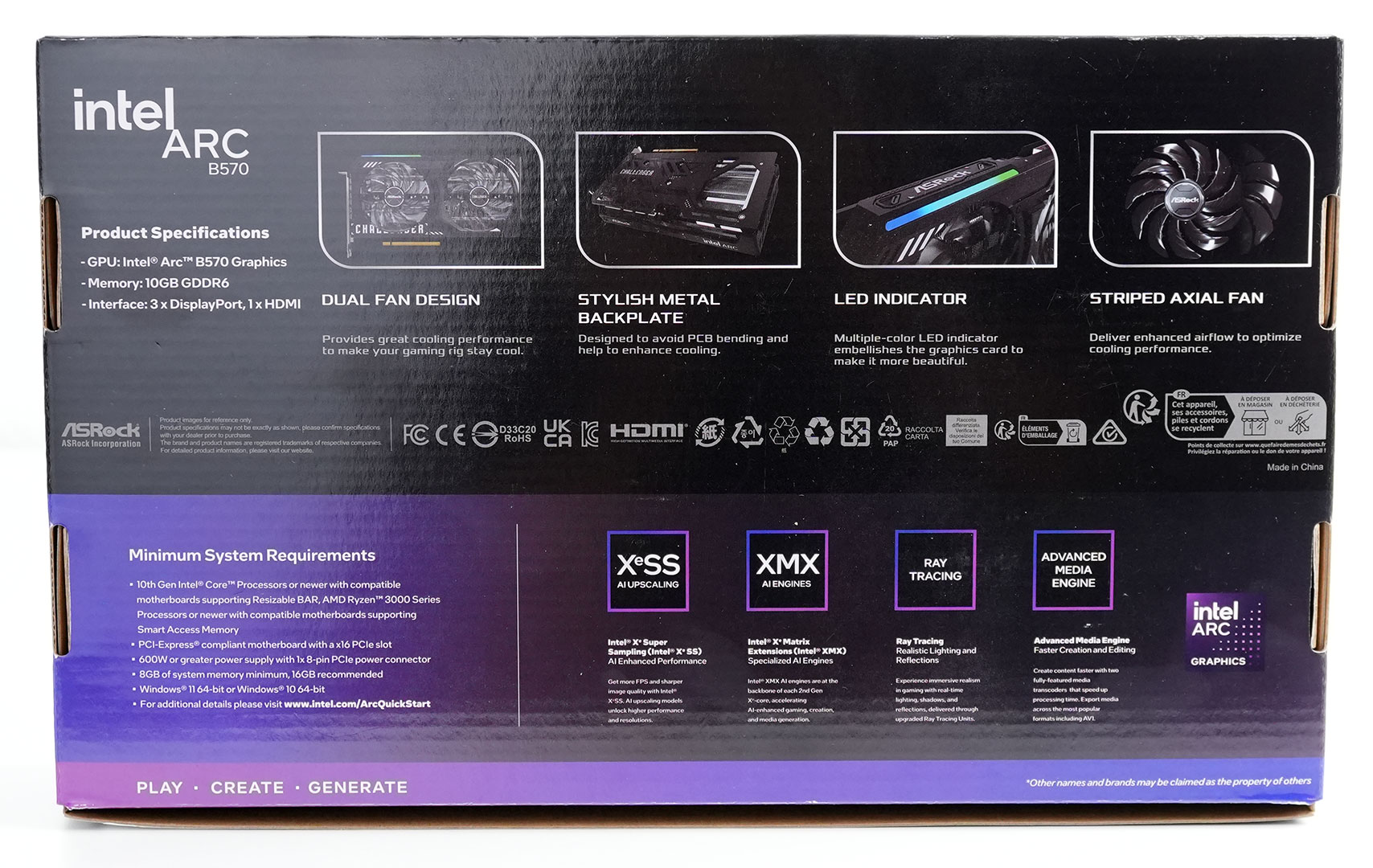
The Arc B570 is based on the same 5 nm BMG-G21 silicon as the B580, but is further cut down. It has 18 Xe cores compared to the 20 on the B580, which work out to 112 execution units, or 2,240 unified shaders. You also get 18 ray tracing units, and 144 XMX cores, 144 TMUs, and 60 ROPs. The memory size is down to 10 GB from the 12 GB on the B580, and the memory bus width is lowered to 160-bit compared to the 192-bit of the B580. Intel is using 19 Gbps GDDR6 memory speeds, and so this results in 380 GB/s of memory bandwidth. This is still a superior memory sub-system to the RTX 4060 and RX 7600, which feature 8 GB of memory across narrower 128-bit memory interfaces. The display and media acceleration capabilities of the Arc B570 are carried over from the B580—you get DisplayPort up to UHBR13.5 and HDMI 2.1 handling I/O, and dual media acceleration engines capable of AV1 and HEVC encode and decode.
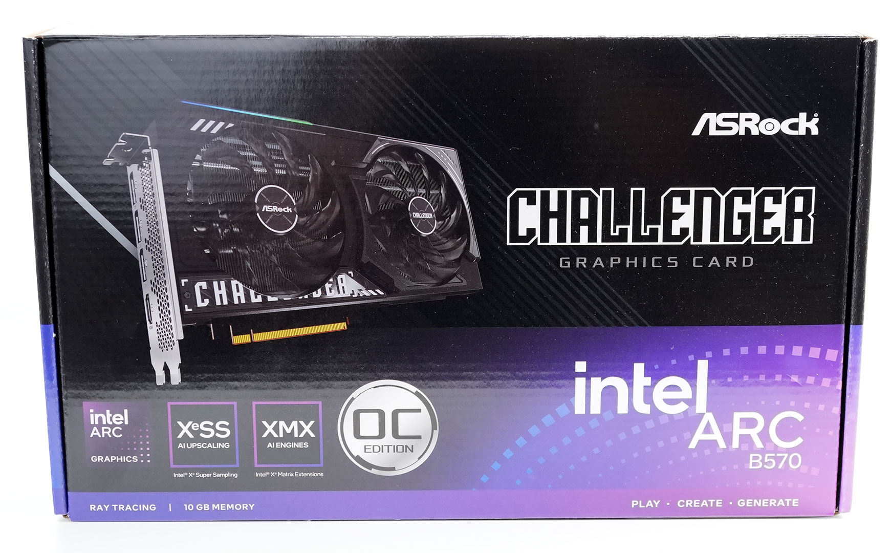
The ASRock Arc B570 Challenger OC is the company's value custom-design based on this GPU, it features a simple aluminium fin-stack heatsink that's ventilated by a pair of large fans that offer idle fan-stop. There's also a well-designed metal 3-D backplate. The PCB underneath is two-thirds the length of the card, and so airflow from the second fan goes through the heatsink and is vented from large cutouts in the backplate. The card draws power from a single 8-pin PCIe power connector. ASRock is pricing the card at a $10 premium over the Intel baseline price, attempting to justify it with a small factory overclock of 2.60 GHz engine clock compared to 2.50 GHz Intel reference, while leaving the memory untouched at 19 Gbps.
| Price | Cores | ROPs | Core Clock | Boost Clock | Memory Clock | GPU | Transistors | Memory | |
|---|---|---|---|---|---|---|---|---|---|
| RX 6500 XT | $140 | 1024 | 32 | 2685 MHz | 2825 MHz | 2248 MHz | Navi 24 | 5400M | 4 GB, GDDR6, 64-bit |
| Arc A580 | $180 | 3072 | 96 | 1700 MHz | N/A | 2000 MHz | ACM-G10 | 21700M | 8 GB, GDDR6, 256-bit |
| RTX 3050 | $165 | 2560 | 32 | 1552 MHz | 1777 MHz | 1750 MHz | GA106 | 12000M | 8 GB, GDDR6, 128-bit |
| Arc A750 | $220 | 3584 | 112 | 2050 MHz | N/A | 2000 MHz | ACM-G10 | 21700M | 8 GB, GDDR6, 256-bit |
| RX 6600 XT | $205 | 2048 | 64 | 2359 MHz | 2589 MHz | 2000 MHz | Navi 23 | 11060M | 8 GB, GDDR6, 128-bit |
| RTX 3060 | $220 | 3584 | 48 | 1320 MHz | 1777 MHz | 1875 MHz | GA106 | 12000M | 12 GB, GDDR6, 192-bit |
| RX 7600 | $250 | 2048 | 64 | 2250 MHz | 2625 MHz | 2250 MHz | Navi 33 | 13300M | 8 GB, GDDR6, 128-bit |
| Arc B570 | $220 | 2304 | 80 | 2500 MHz | N/A | 2375 MHz | BMG-G21 | 19600M | 10 GB, GDDR6, 160-bit |
| ASRock Arc B570 Challenger OC | $230 | 2304 | 80 | 2600 MHz | N/A | 2375 MHz | BMG-G21 | 19600M | 10 GB, GDDR6, 160-bit |
| RX 7600 XT | $310 | 2048 | 64 | 2470 MHz | 2755 MHz | 2250 MHz | Navi 33 | 13300M | 16 GB, GDDR6, 128-bit |
| RTX 4060 | $285 | 3072 | 48 | 1830 MHz | 2460 MHz | 2125 MHz | AD107 | 18900M | 8 GB, GDDR6, 128-bit |
| Arc A770 | $250 | 4096 | 128 | 2100 MHz | N/A | 2187 MHz | ACM-G10 | 21700M | 16 GB, GDDR6, 256-bit |
| Arc B580 | $250 | 2560 | 80 | 2670 MHz | N/A | 2375 MHz | BMG-G21 | 19600M | 12 GB, GDDR6, 192-bit |
| RTX 3060 Ti | $300 | 4864 | 80 | 1410 MHz | 1665 MHz | 1750 MHz | GA104 | 17400M | 8 GB, GDDR6, 256-bit |
| RTX 4060 Ti | $380 | 4352 | 48 | 2310 MHz | 2535 MHz | 2250 MHz | AD106 | 22900M | 8 GB, GDDR6, 128-bit |
| RX 6700 XT | $350 | 2560 | 64 | 2424 MHz | 2581 MHz | 2000 MHz | Navi 22 | 17200M | 12 GB, GDDR6, 192-bit |
| RTX 3070 | $320 | 5888 | 96 | 1500 MHz | 1725 MHz | 1750 MHz | GA104 | 17400M | 8 GB, GDDR6, 256-bit |
| RTX 3070 Ti | $370 | 6144 | 96 | 1575 MHz | 1770 MHz | 1188 MHz | GA104 | 17400M | 8 GB, GDDR6X, 256-bit |
| RX 6800 | $340 | 3840 | 96 | 1815 MHz | 2105 MHz | 2000 MHz | Navi 21 | 26800M | 16 GB, GDDR6, 256-bit |
| RX 7700 XT | $370 | 3456 | 96 | 2171 MHz | 2544 MHz | 2250 MHz | Navi 32 | 26500M | 12 GB, GDDR6, 192-bit |
| RX 6800 XT | $400 | 4608 | 128 | 2015 MHz | 2250 MHz | 2000 MHz | Navi 21 | 26800M | 16 GB, GDDR6, 256-bit |
Xe2 Battlemage Architecture
The Arc B580 debuted Intel's second discrete gaming GPU architecture, codenamed Xe2 "Battlemage," in December 2024, and the new Arc B570 is the second discrete GPU based on it. A variant of Xe2 is used in the integrated graphics solution of Intel's Core Ultra 200V "Lunar Lake" mobile processors, the one today is its fully-fledged discrete gaming GPU version, with all hardware components enabled. The Arc B570 is a mid-range model based on the BMG-G21 silicon. The B570 is further cut down from the B580, which itself doesn't appear to max out the BMG-G21 silicon it is based on. The BMG-G21 is built on the TSMC N5 (5 nm EUV) foundry node, and packs 19.6 billion transistors across a 272 mm² monolithic die. The 5 nm node is contemporary, given that both NVIDIA "Ada" and AMD RDNA 3 gaming GPUs use it.
The BMG-G21 GPU features a PCI-Express 4.0 x8 host interface on the Arc B580 and B570. It is configured with a 192-bit GDDR6 memory bus on the B580, and a 160-bit bus on the B570. The GPU is organized in a very similar manner to modern GPUs from NVIDIA and AMD—a Global Dispatch processor distributes work among the five Render Slices, which talk to each other over the GPU's fabric and memory sub-system. The GPU's internal last-level cache is 18 MB in size. Besides the five Render Slices, there is the Media Engine, consisting of two MFX multi-format x-coders (encoders/decoders); and there are two sets of hardware encoders and decoders. Then there's the GDDR6 memory controller and the Display Engine, with four display interfaces.
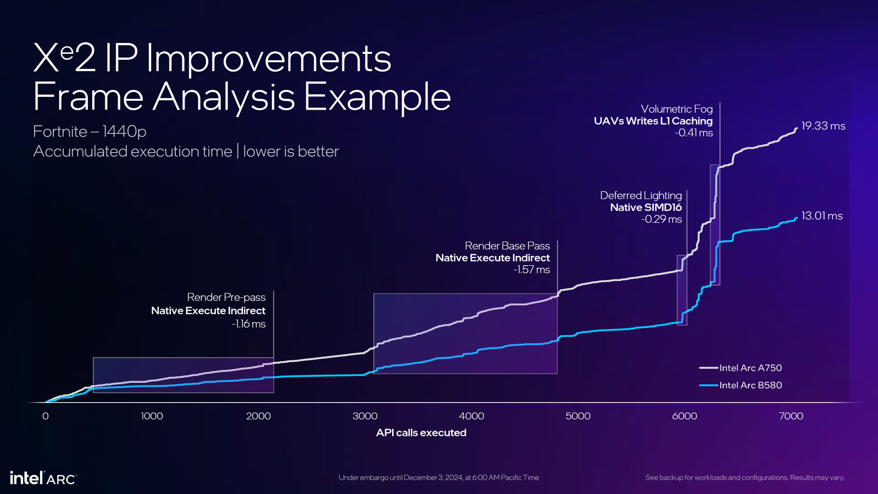
Intel is claiming a 70% generational increase in performance per Xe Core, the indivisible number-crunching subunit of the GPU; and a 50% generational performance-per-watt increase. The above graphs illustrate the contribution of the individual sub-systems of the Xe2 Battlemage architecture toward these improvements; and how this plays out in a frametime analysis example of a real-world use case.
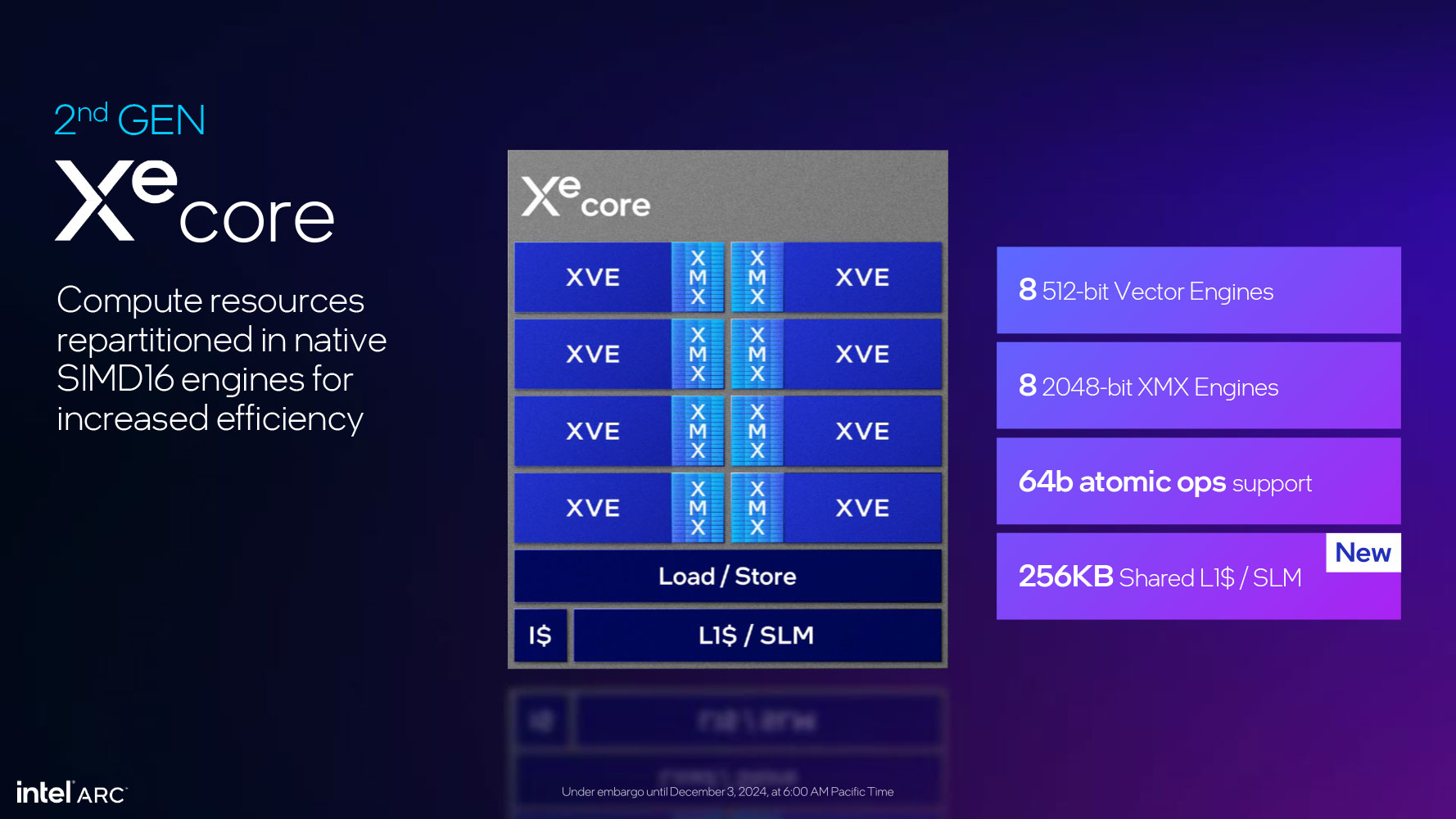

The Render Slice diagram (above) highlights the biggest chunk of the generational performance increase by Intel. It's thanks to increased IPC from the Xe Core, a more specialized and capable Ray Tracing Unit, a 300% faster Geometry engine, faster Sampler, 50% increase in HiZ, Z, stencil caches, and increases in performance of the pixel backends. Intel's engineering goal has been to reduce latency wherever it can, and reduce software (CPU) overhead as much as it can. The new second gen Xe Core features eight 512-bit vector engines, with SIMD16-native ALUs, and many more data formats. Rather than two sets of FP and INT units per vector engine, there is just one set of each per vector engine in Xe2, with larger numbers of ALUs.
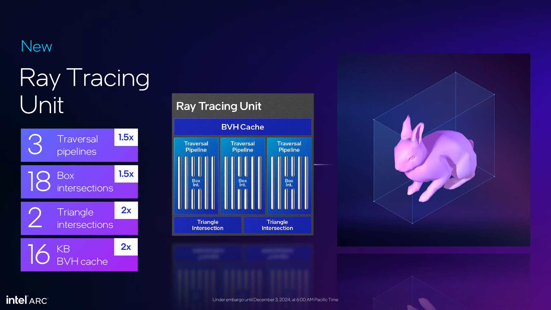
Intel introduced its second gen Ray Tracing Unit, with massive generational improvements in performance and capability. It introduces a third Traversal Pipeline, which yields a 50% increase in box intersection performance. A second triangle intersection unit has been added to double the performance of triangle intersections. The BVH cache has doubled in size to 16 KB.
XeSS 2, Frame Generation, and Low Latency
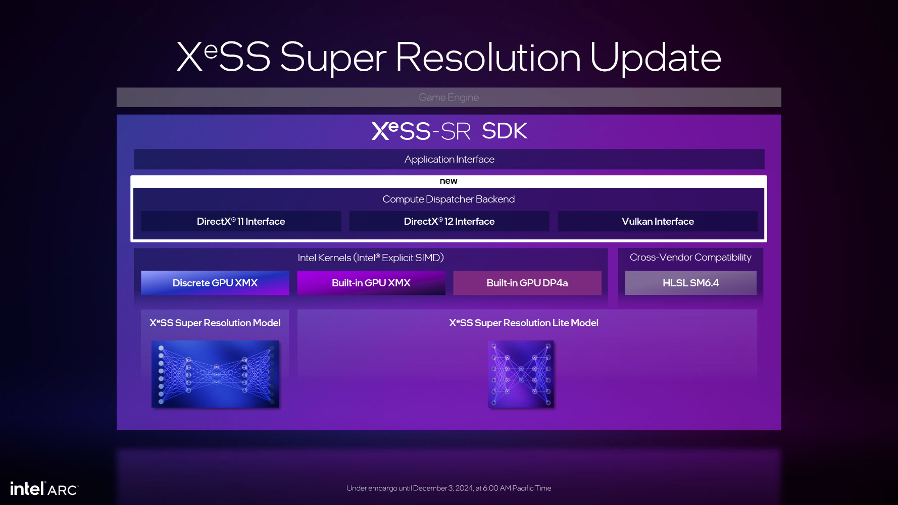

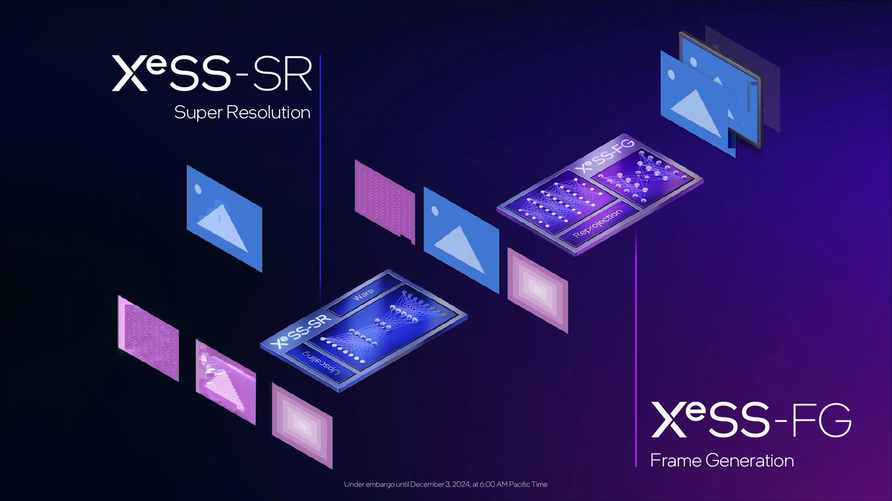
Intel has codified the original XeSS as XeSS Super Resolution (XeSS-SR), as that's what it originally was—a performance enhancement that relies on super-resolution technology. The XeSS-SR SDK gets a new compute dispatcher backend for popular APIs—DirectX 11, DirectX 12, and Vulkan. There are two XeSS-SR models, the regular one, and a XeSS-SR Lite model for GPUs that lack XMX matrix acceleration capability.
XeSS 2 isn't a single technology, or an improvement over XeSS-SR, but a collection of three technologies—the existing XeSS-SR, which deals with performance; the new XeSS Frame Generation (XeSS-FG) technology, which nearly doubles frame rates based on intelligent frame doubling; and the new Xe Low Latency (XeLL) technology, which works to reduce the latency cost of SR and FG, but is something that can be used as a standalone whole-system latency technology, too.
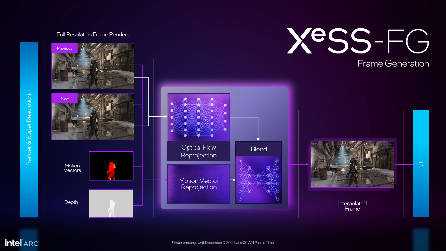
XeSS-FG can either be implemented at native resolution, or in conjunction with XeSS-SR, where it is located right after the XeSS-SR step in the rendering queue. It relies on motion vectors, depth data, temporal frame data, and optical flow reprojection, to create interpolated frames that are then interleaved with the output frames, to effectively double the framerate. The interpolated image is then passed along to the next stage, where the HUD/UI is added at native resolution, and pushed to the frame buffer for output.
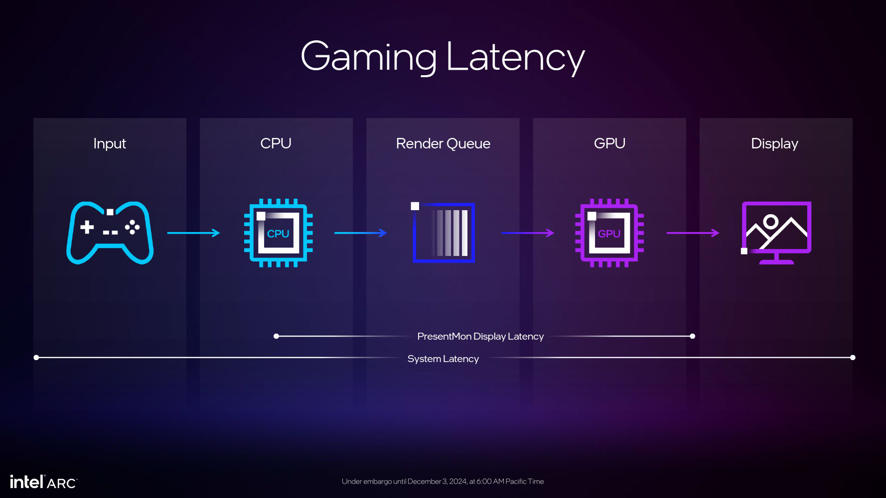
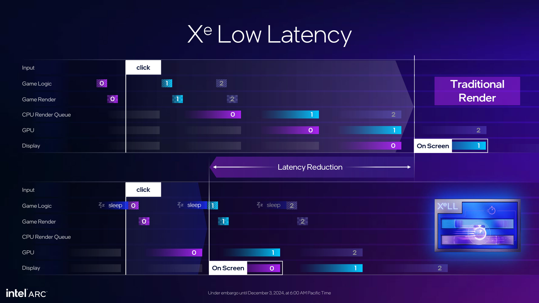
The SR + FG passes contribute to frame latency, and so, just as NVIDIA uses Reflex to counteract this latency, Intel innovated XeLL. The technology intelligently compacts the rendering queue to reduce the time it takes for an input to register as motion on-screen. XeLL remains enabled in all workloads the use XeSS-FG, but it can be used as a standalone feature, too. There's also an implicit driver-based low-latency mode that does this without a game having an explicit XeSS 2 or XeLL implementation.
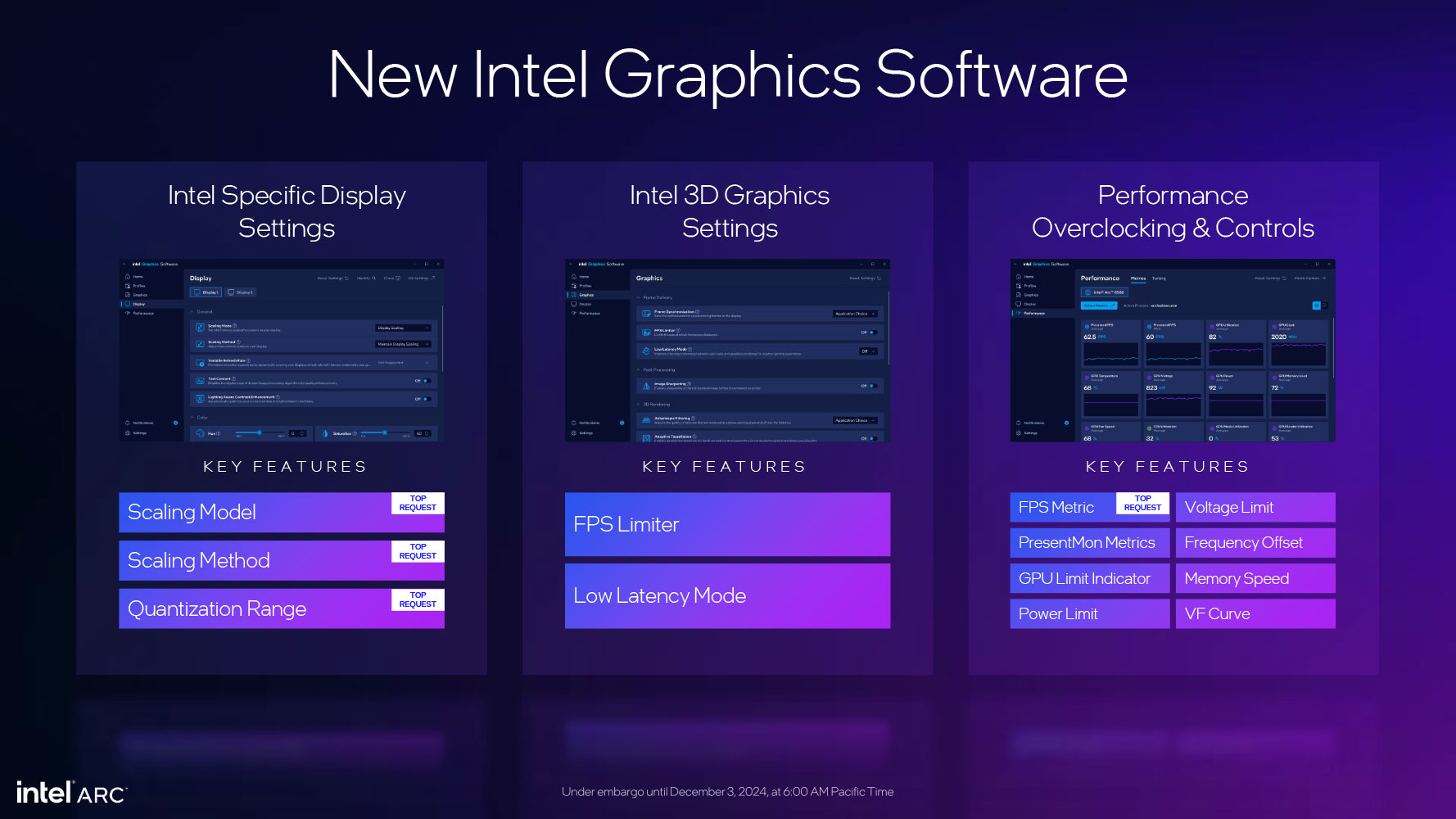
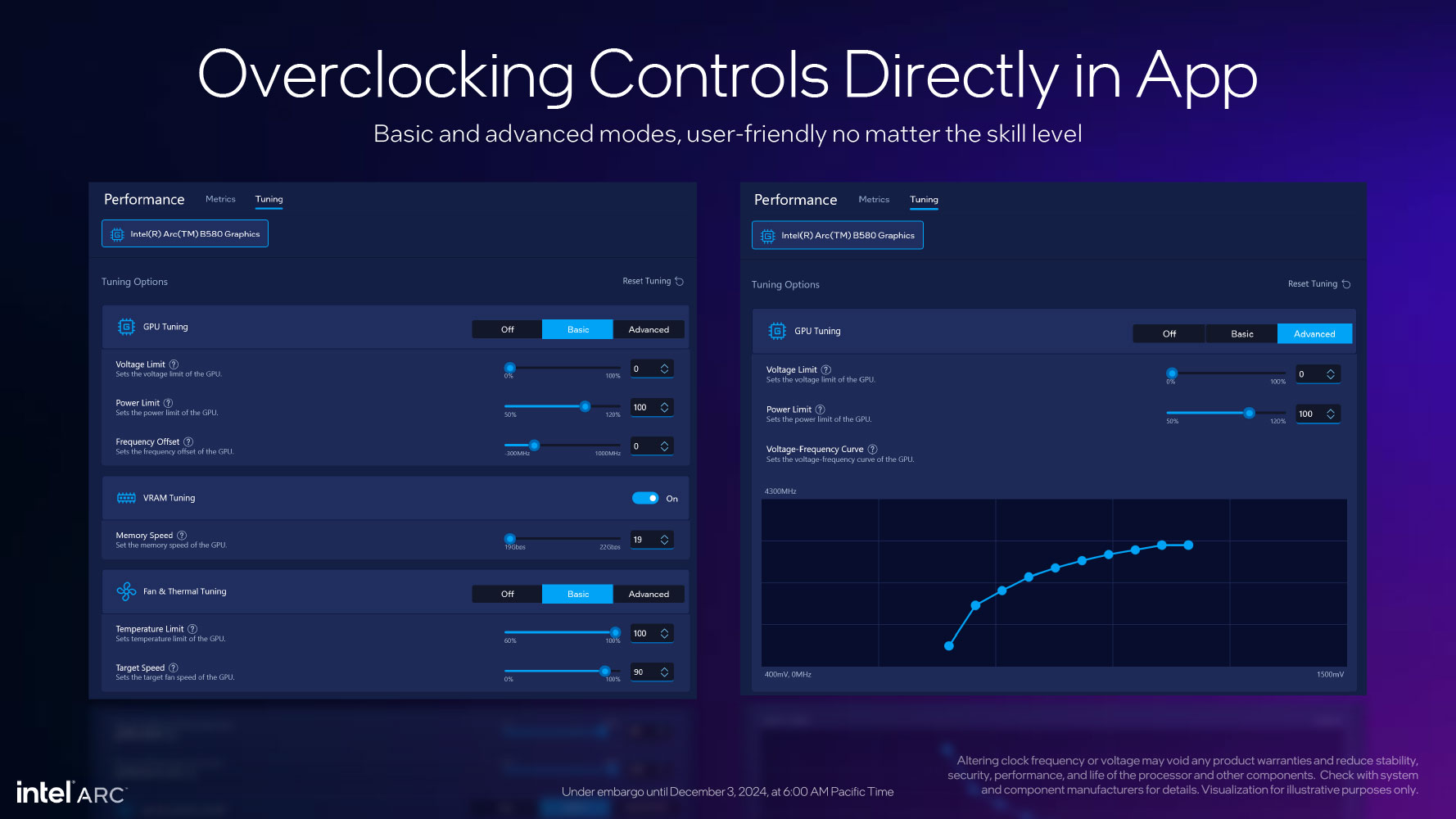
Intel has updated its software package significantly. The new "Intel Graphics Software" replaces the "Arc Control" utility, and gives you a cleaner user interface. There are many new settings related to the display, including display scaling model/method/quantization range; 3D graphics settings, including a driver-based FPS limiter, the driver-based low-latency mode; and the exhaustive new Performance and Overclocking controls, which include the ability to set frequency offsets, tinker with the V/F curve, power limits, and GPU and memory clocks. It also integrates Intel's PresentMon metrics.
Packaging
The Card
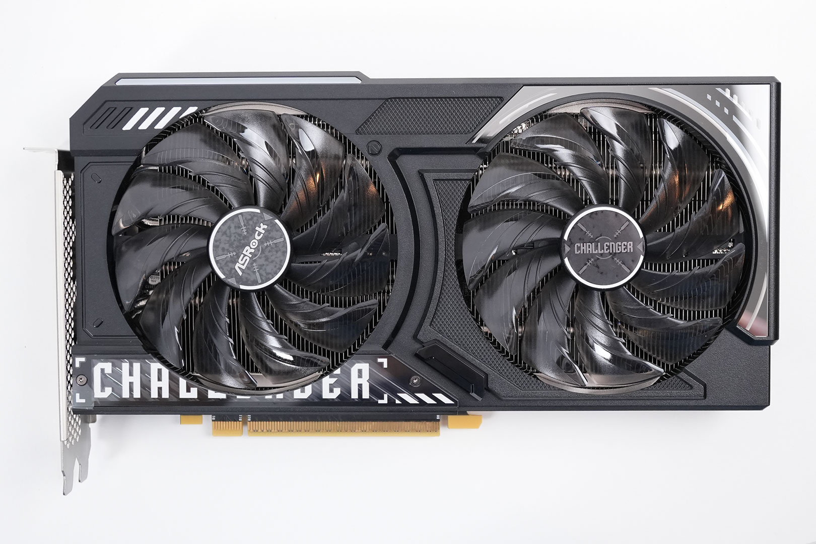
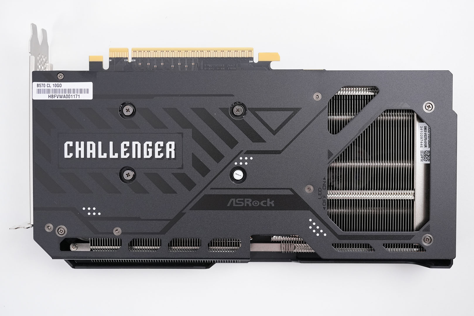
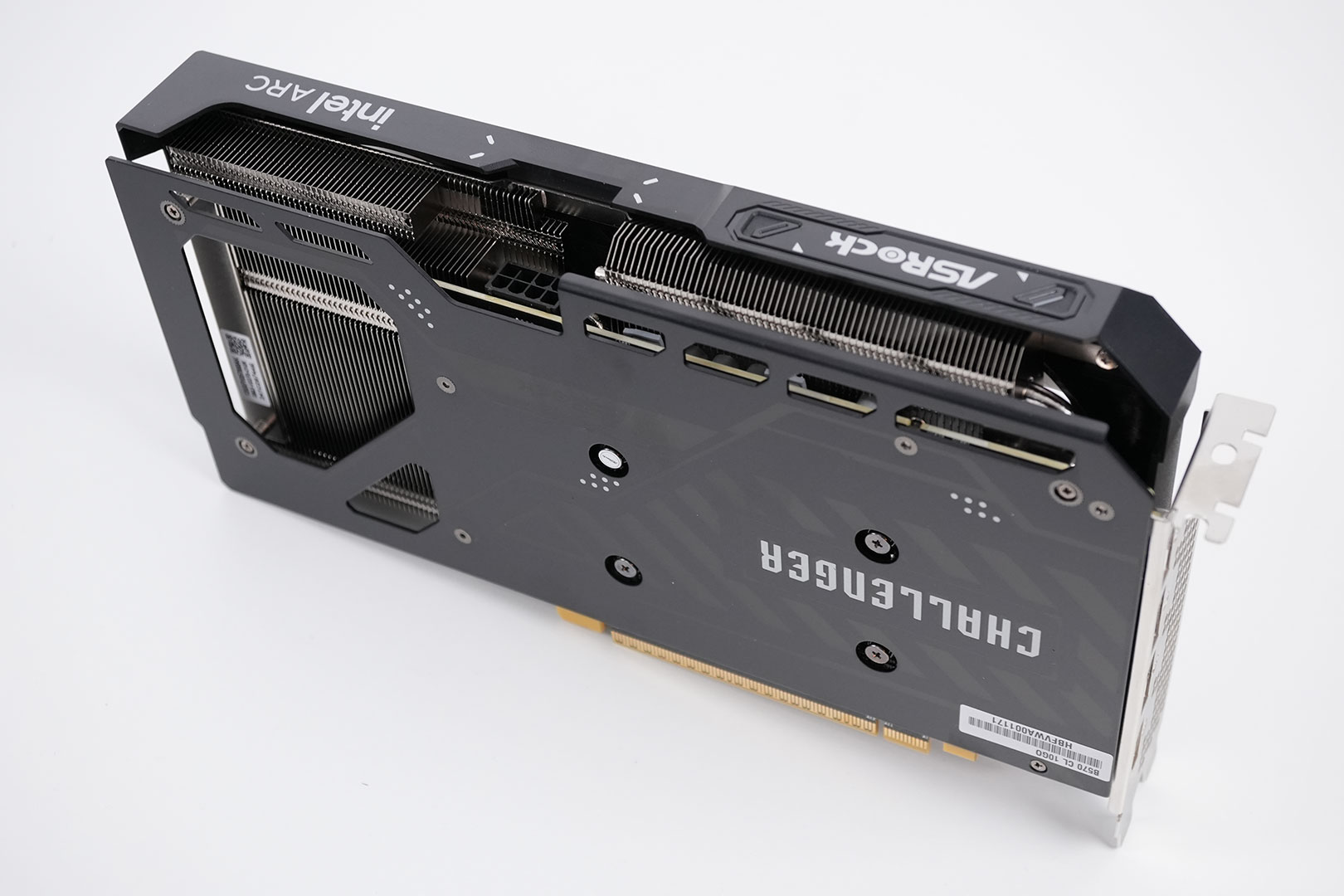
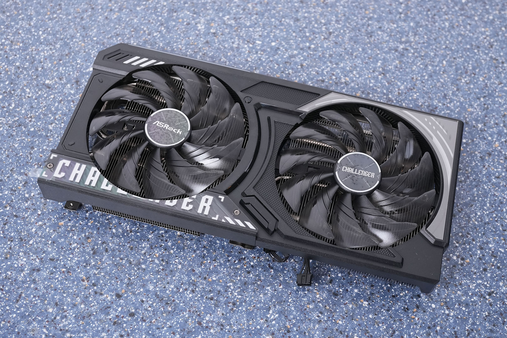
ASRock's card comes with a mostly-black color theme that has white and shiny highlights. The card uses a short PCB, which allows some airflow through the card for better cooling performance. On the back you get a metal backplate, which integrates nicely with the rest of the design.
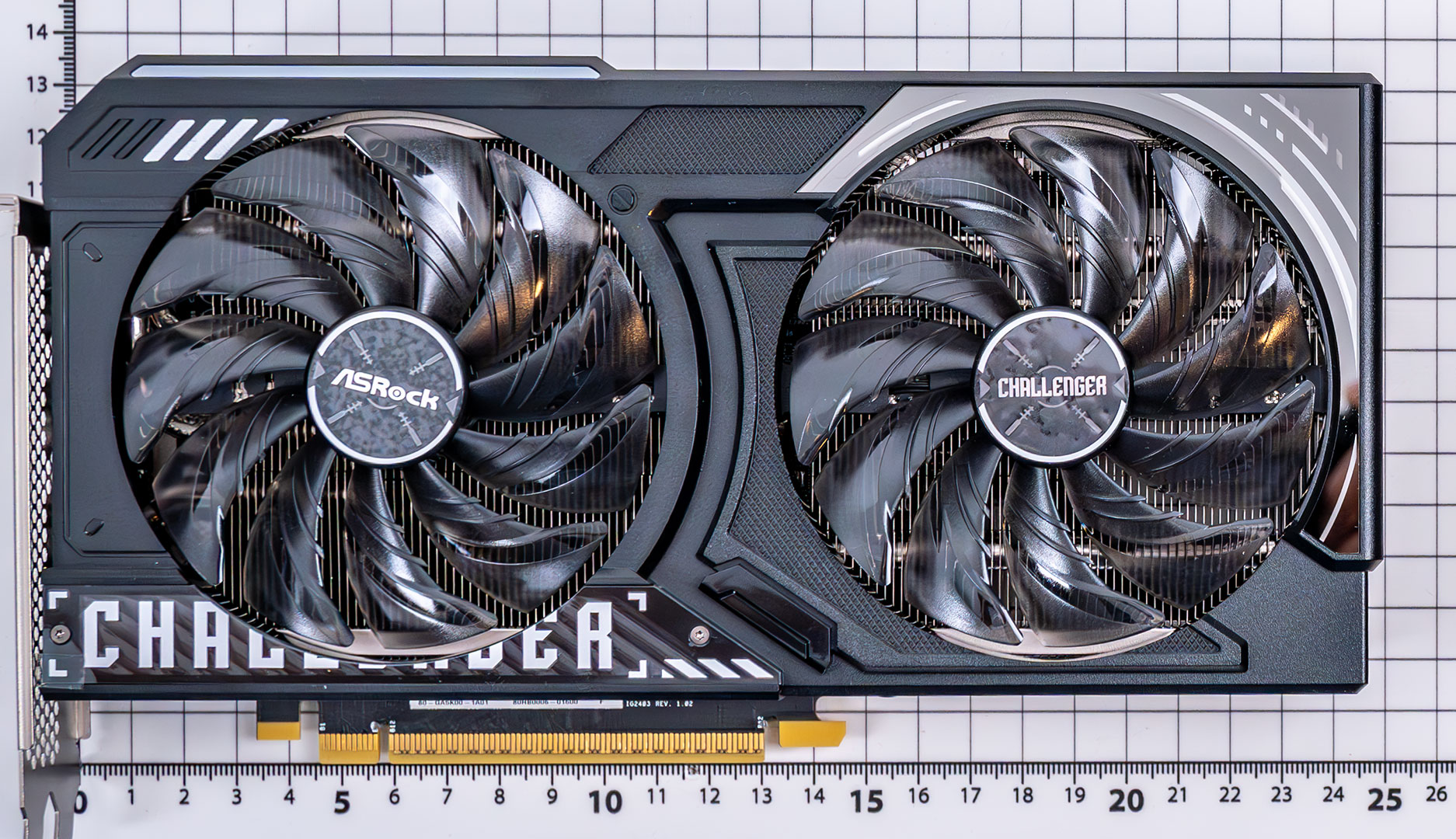
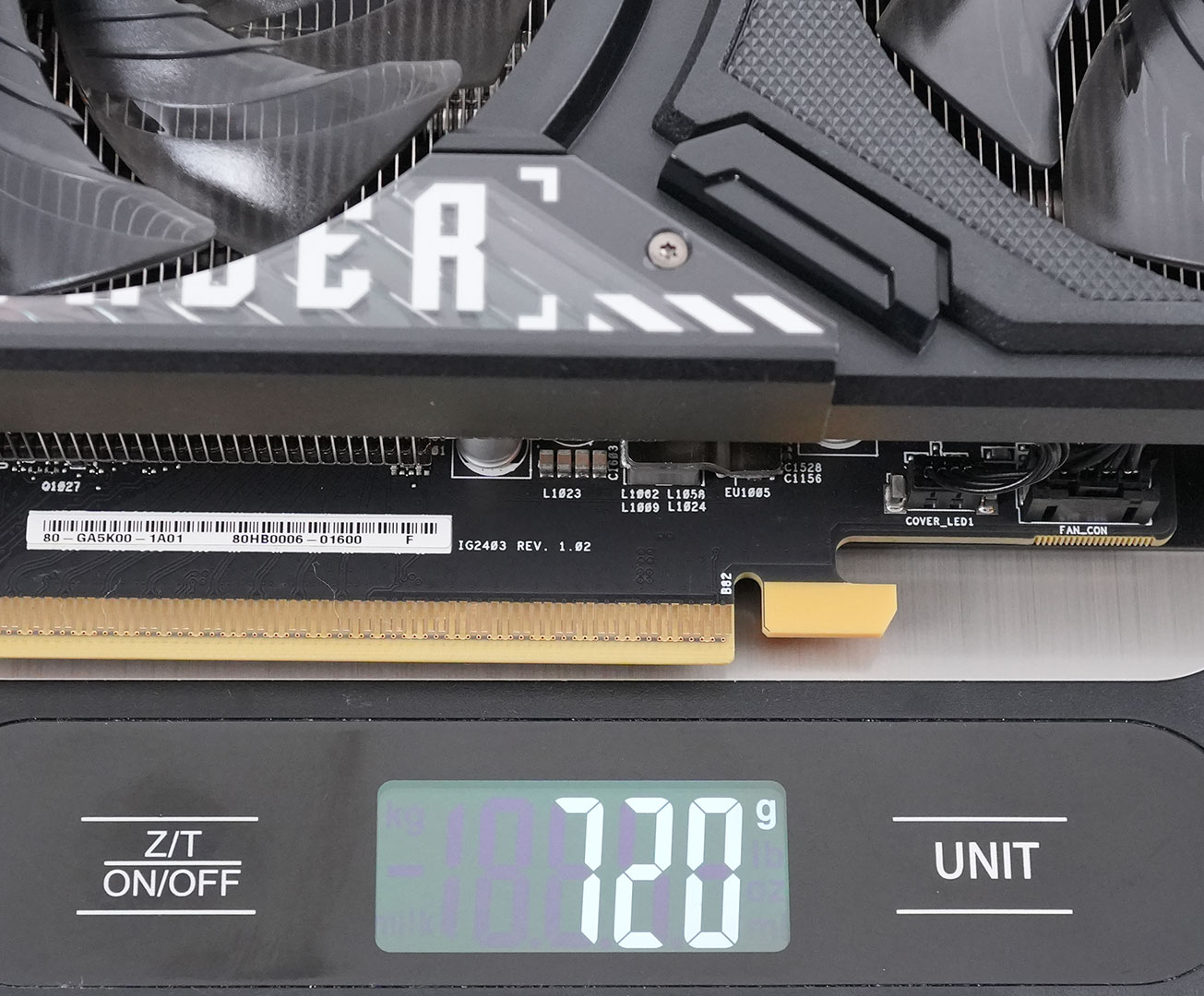
Dimensions of the card are 25.0 x 13.5 cm, and it weighs 720 g.
Installation requires two slots in your system. We measured the card's width to be 40 mm.
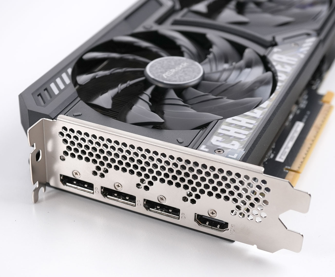
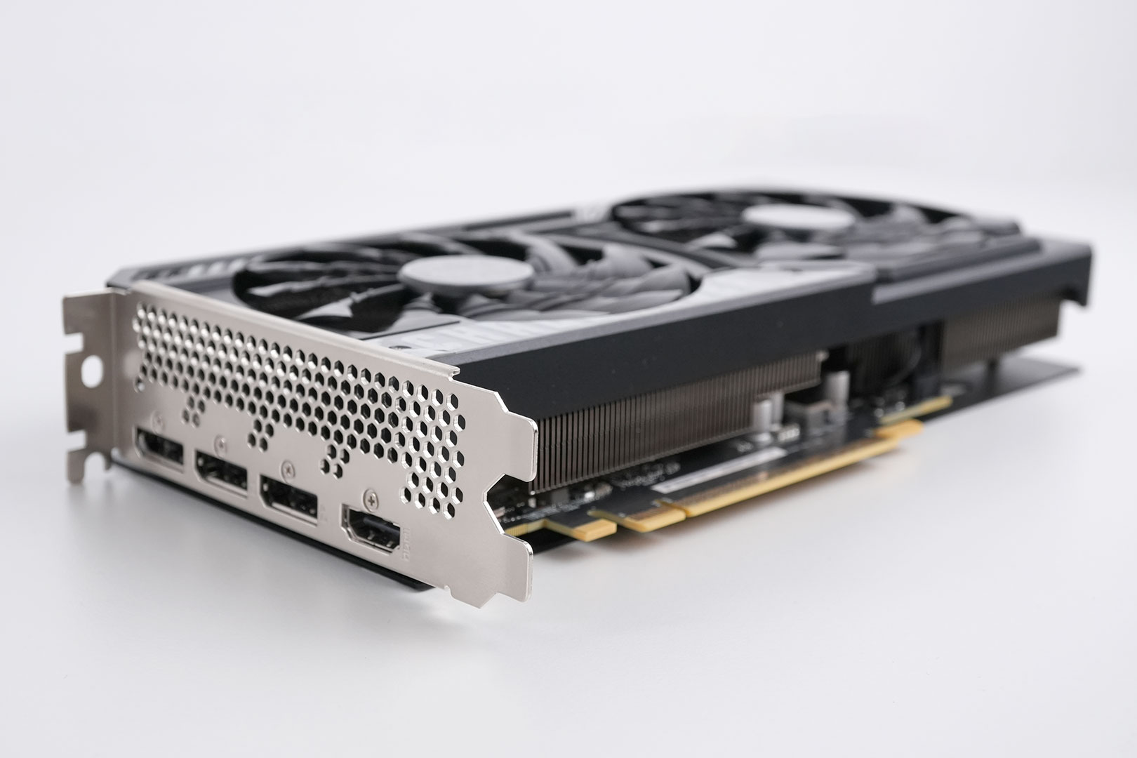
Display connectivity includes three standard DisplayPort 2.1 and one HDMI 2.1a. On the Intel reference card one port is marked with a black outline, but not on this card. That port supports higher bitrates (UHBR13.5), i.e. 4K up to 360 Hz, while the other two ports support up to 240 Hz, so I guess you have to test them to find the right one (if you have a monitor that requires such high transfer rates).
In terms of codecs, you get full support for H.264, H.265, VP9 and AV1, both encode and decode. Worth highlighting is HEVC 4:2:2 10-bit encoding and decoding, which is a unique capability, and AV1 Screen Content encoding, which improves the quality of text in movies—fantastic for screen recordings or screen sharing.
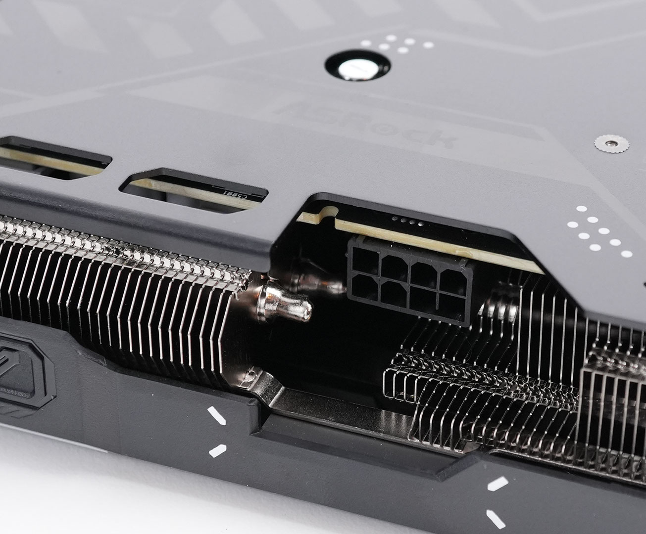
The card uses a single 8-pin connector, plus PCIe slot power, allowing a maximum power draw of 225 W.
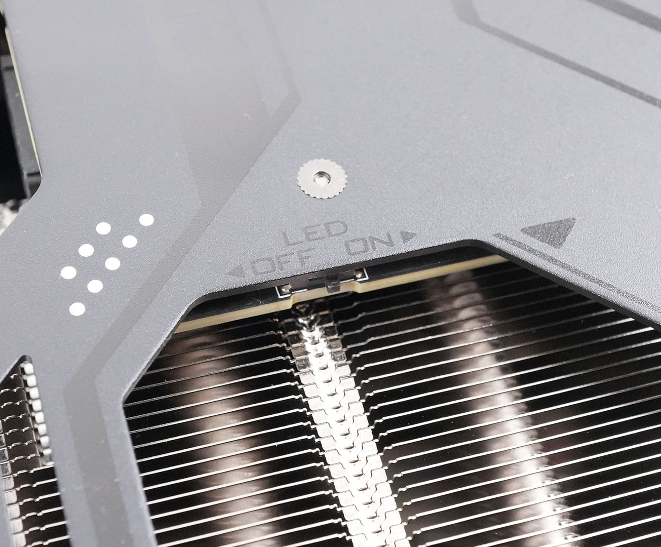
If you prefer, the lighting can be turned off easily with this switch—no software required.
Teardown
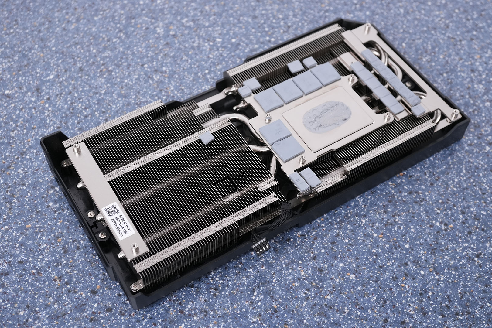
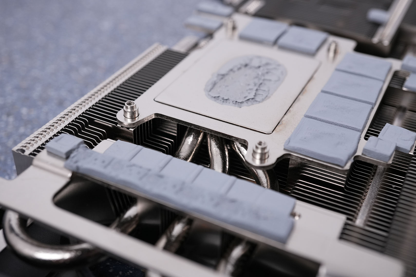
The main cooler uses three heatpipes and provides cooling for the GPU, memory and VRM circuitry.
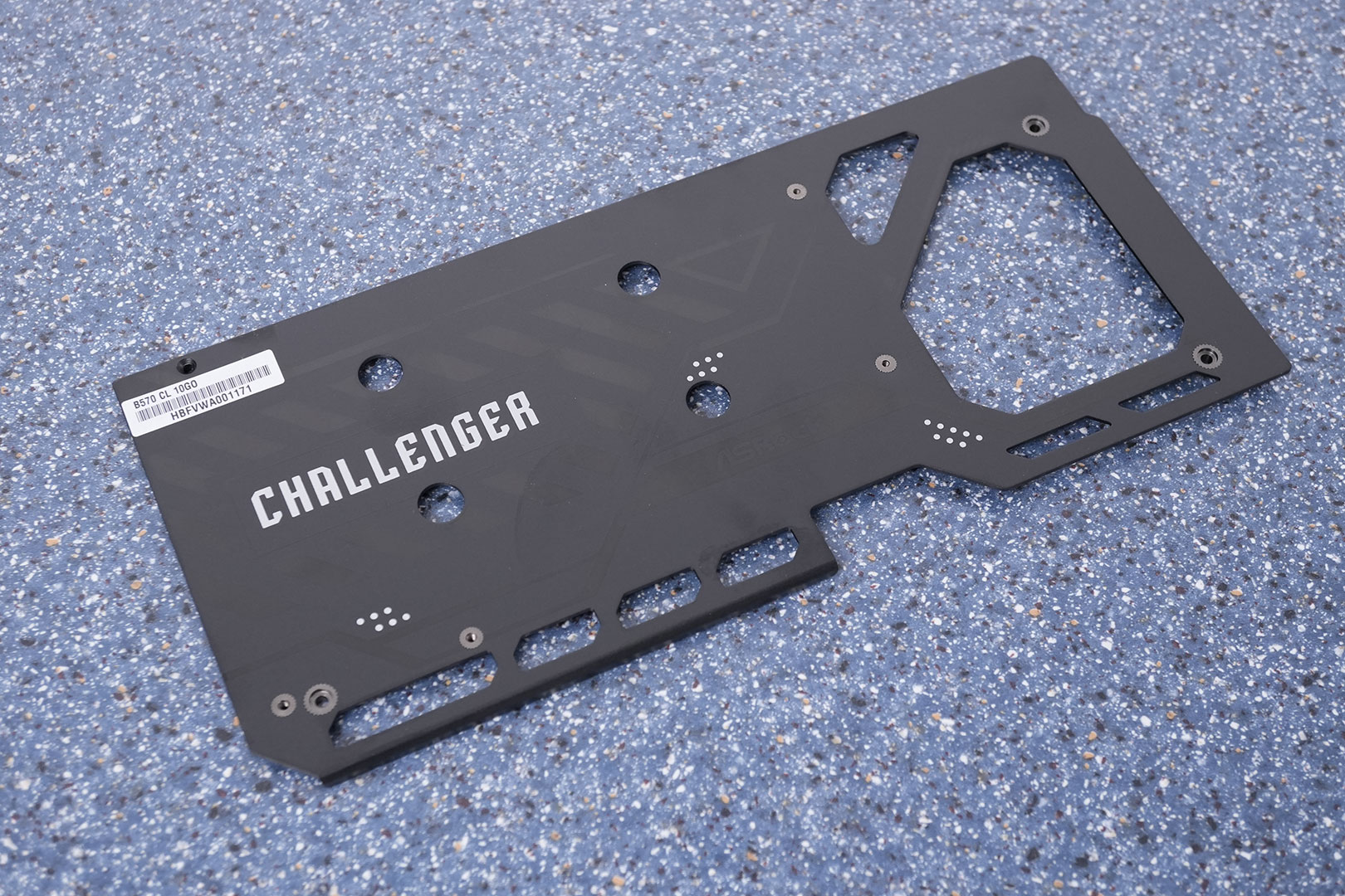
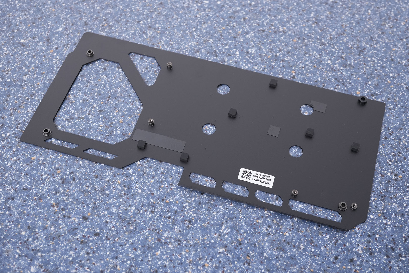
On the back, you'll find a metal backplate with a cutout to improve airflow.
Our Patreon Silver Supporters can read articles in single-page format.
Mar 25th, 2025 15:44 EDT
change timezone
Latest GPU Drivers
New Forum Posts
- Hotspot 110° (1)
- Did Nvidia purposely gimp the performance of 50xx series cards with drivers (16)
- Brand new 9950x3d crashing after a few minutes of AIDA64 CPU + FPU stress test (9)
- What are you playing? (23265)
- What's your latest tech purchase? (23394)
- What is going to be your next tech upgrade? just curious :) (8)
- Milestones (14009)
- Do you use Linux? (548)
- Motherboard for home/business NAS, which one should I get? (0)
- Lenovo ThinkPad L15 Gen 1 (AMD) - DRAM soldered? (9)
Popular Reviews
- Assassin's Creed Shadows Performance Benchmark Review - 30 GPUs Compared
- be quiet! Pure Rock Pro 3 Black Review
- ASUS ProArt X870E-Creator Wi-Fi Review
- ASRock Radeon RX 9070 XT Taichi OC Review - Excellent Cooling
- Sapphire Radeon RX 9070 XT Nitro+ Review - Beating NVIDIA
- ASUS GeForce RTX 5070 TUF OC Review
- AMD Ryzen 9 9950X3D Review - Great for Gaming and Productivity
- AMD Ryzen 7 9800X3D Review - The Best Gaming Processor
- Quick Look: Jelly Key Mystic Snake Artisan Keycaps
- Pulsar Feinmann F01 Review
Controversial News Posts
- AMD RDNA 4 and Radeon RX 9070 Series Unveiled: $549 & $599 (260)
- AMD Radeon RX 9070-series Pricing Leaks Courtesy of MicroCenter (158)
- MSI Doesn't Plan Radeon RX 9000 Series GPUs, Skips AMD RDNA 4 Generation Entirely (142)
- Microsoft Introduces Copilot for Gaming (123)
- AMD Radeon RX 9070 XT Reportedly Outperforms RTX 5080 Through Undervolting (118)
- NVIDIA Reportedly Prepares GeForce RTX 5060 and RTX 5060 Ti Unveil Tomorrow (115)
- Over 200,000 Sold Radeon RX 9070 and RX 9070 XT GPUs? AMD Says No Number was Given (100)
- NVIDIA GeForce RTX 5050, RTX 5060, and RTX 5060 Ti Specifications Leak (96)