 60
60
ASRock Radeon RX 7900 XTX Taichi Review
(60 Comments) »Introduction
ASRock Radeon RX 7900 XTX Taichi is the company's flagship air-cooled graphics card powered by AMD's fastest RDNA 3 GPU. An established player in the motherboard space, ASRock entered the graphics card business as an AMD partner just two generations ago, and now leads the space with some of the most powerful custom graphics card designs. The RX 7900 XTX Taichi retains the high-quality industrial product-design language of the brand, and serves up a powerful cooling solution, paired with an overclocker-grade PCB for the RX 7900 XTX. In particular, it has a third 8-pin power connector that expands the power-limit, letting the the flagship GPU stretch its legs better, and offer better overclocking.
The Radeon RX 7900 XTX debuts the RDNA 3 graphics architecture, with silicon-level innovation that's as profound as the company's Ryzen 3000 desktop processors--disaggregation. AMD is maximizing its allocation of the TSMC 5 nm EUV node, by building a centralized die that contains only those components that benefit the most from the switch to 5 nm-- the GPU's main number-crunching and graphics rendering machinery. The company identified two key components that don't benefit that much with 5 nm, namely the memory controllers, GDDR6 PHY, and the Infinity Cache memory, and split them out into separate dies called MCDs (memory cache dies), built on 6 nm. There are six of these on the "Navi 31" GPU powering the RX 7900 XTX, each with a 64-bit wide GDDR6 memory path, and a 16 MB slice of the GPU's 96 MB of Infinity Cache. These make up the GPU's 384-bit memory interface, and AMD could carve out SKUs such as the RX 7900 XT that have a narrower 320-bit bus, by simply disabling one of the six MCDs.

The new RDNA 3 graphics architecture introduces a faster dual-issue rate compute unit that supports new math formats, comes with AI acceleration hardware besides 2nd Gen Ray Accelerators that support 50% higher ray-intersection performance. AMD claims a 17.5% IPC gain for its RDNA 3 CU, which when combined with the 20% higher CU count, higher clock-speeds, and 87% higher memory bandwidth, adds up to a 51% generational performance/Watt uplift, making the RX 7900 XTX competitive with some of NVIDIA's fastest GPUs, such as the GeForce RTX 4080, which it undercuts in pricing by as much as $200 (at least when looking at MSRPs).
The most surprising aspect of the RX 7900 XTX is its power configuration, with a stock power limit of just 350 W, that's open to be increased on custom-design cards such as the ASRock Taichi we're reviewing today. It's possible to build cards with just two 8-pin PCIe power connectors, without the need for a fancy power adapter. The ASRock Taichi features three 8-pin connectors for a 525 W maximum power input capability. This enabled ASRock to increase GPU clock speeds from 2300/2500 MHz reference, to 2510/2680 MHz.
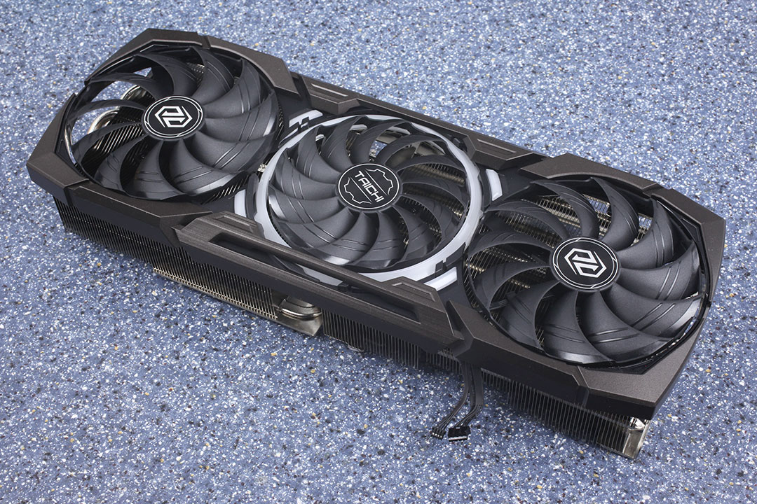
The ASRock RX 7900 XTX Taichi debuts the company's latest Taichi 3X cooling solution that uses three massive 110 mm fans, a heavy dual aluminium fin-stack heatsink, eight heatpipes, and a dedicated memory heatpipe. The card offers a powerful 22-phase VRM that draws power from three 8-pin PCIe power connectors; and offers goodies such as dual-BIOS, addressable RGB headers, etc. ASRock is pricing the card at USD $1120, a $120 premium over the $1000 baseline price.
| Price | Cores | ROPs | Core Clock | Boost Clock | Memory Clock | GPU | Transistors | Memory | |
|---|---|---|---|---|---|---|---|---|---|
| RTX 2080 Ti | $420 | 4352 | 88 | 1350 MHz | 1545 MHz | 1750 MHz | TU102 | 18600M | 11 GB, GDDR6, 352-bit |
| RTX 3070 | $400 | 5888 | 96 | 1500 MHz | 1725 MHz | 1750 MHz | GA104 | 17400M | 8 GB, GDDR6, 256-bit |
| RTX 3070 Ti | $520 | 6144 | 96 | 1575 MHz | 1770 MHz | 1188 MHz | GA104 | 17400M | 8 GB, GDDR6X, 256-bit |
| RX 6800 | $480 | 3840 | 96 | 1815 MHz | 2105 MHz | 2000 MHz | Navi 21 | 26800M | 16 GB, GDDR6, 256-bit |
| RX 6800 XT | $560 | 4608 | 128 | 2015 MHz | 2250 MHz | 2000 MHz | Navi 21 | 26800M | 16 GB, GDDR6, 256-bit |
| RTX 3080 | $570 | 8704 | 96 | 1440 MHz | 1710 MHz | 1188 MHz | GA102 | 28000M | 10 GB, GDDR6X, 320-bit |
| RTX 3080 Ti | $750 | 10240 | 112 | 1365 MHz | 1665 MHz | 1188 MHz | GA102 | 28000M | 12 GB, GDDR6X, 384-bit |
| RX 6900 XT | $680 | 5120 | 128 | 2015 MHz | 2250 MHz | 2000 MHz | Navi 21 | 26800M | 16 GB, GDDR6, 256-bit |
| RX 6950 XT | $800 | 5120 | 128 | 2100 MHz | 2310 MHz | 2250 MHz | Navi 21 | 26800M | 16 GB, GDDR6, 256-bit |
| RTX 3090 | $850 | 10496 | 112 | 1395 MHz | 1695 MHz | 1219 MHz | GA102 | 28000M | 24 GB, GDDR6X, 384-bit |
| RTX 4070 Ti | $820 | 7680 | 80 | 2310 MHz | 2610 MHz | 1313 MHz | AD104 | 35800M | 12 GB, GDDR6X, 192-bit |
| RX 7900 XT | $880 | 5376 | 192 | 2000 MHz | 2400 MHz | 2500 MHz | Navi 31 | 57700M | 20 GB, GDDR6, 320-bit |
| RTX 3090 Ti | $1400 | 10752 | 112 | 1560 MHz | 1950 MHz | 1313 MHz | GA102 | 28000M | 24 GB, GDDR6X, 384-bit |
| RTX 4080 | $1200 | 9728 | 112 | 2205 MHz | 2505 MHz | 1400 MHz | AD103 | 45900M | 16 GB, GDDR6X, 256-bit |
| RX 7900 XTX | $1000 | 6144 | 192 | 2300 MHz | 2500 MHz | 2500 MHz | Navi 31 | 57700M | 24 GB, GDDR6, 384-bit |
| ASRock RX 7900 XTX Taichi | $1120 | 6144 | 192 | 2510 MHz | 2680 MHz | 2500 MHz | Navi 31 | 57700M | 24 GB, GDDR6, 384-bit |
| RTX 4090 | $1600 | 16384 | 176 | 2235 MHz | 2520 MHz | 1313 MHz | AD102 | 76300M | 24 GB, GDDR6X, 384-bit |
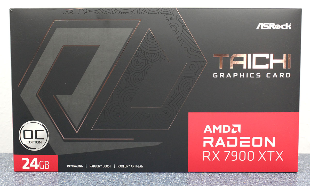
Packaging
The Card

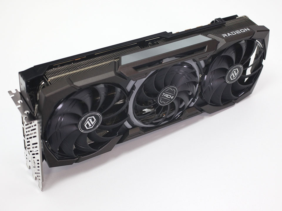
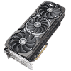
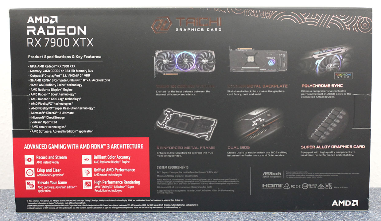
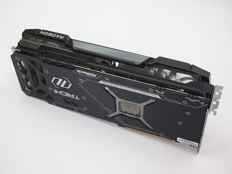
ASRock created a new design for their RX 7900 Series Taichi cooler. They kept the blocky, industrial design of previous Taichi products, but the cogwheel iconography is now only present on the center fan hub. The fan frames are now solid, which helps make the card look less busy. On the metal backplate we get to meet the cogwheel design again, ASRock has added more white highlights here compared to previous generations.

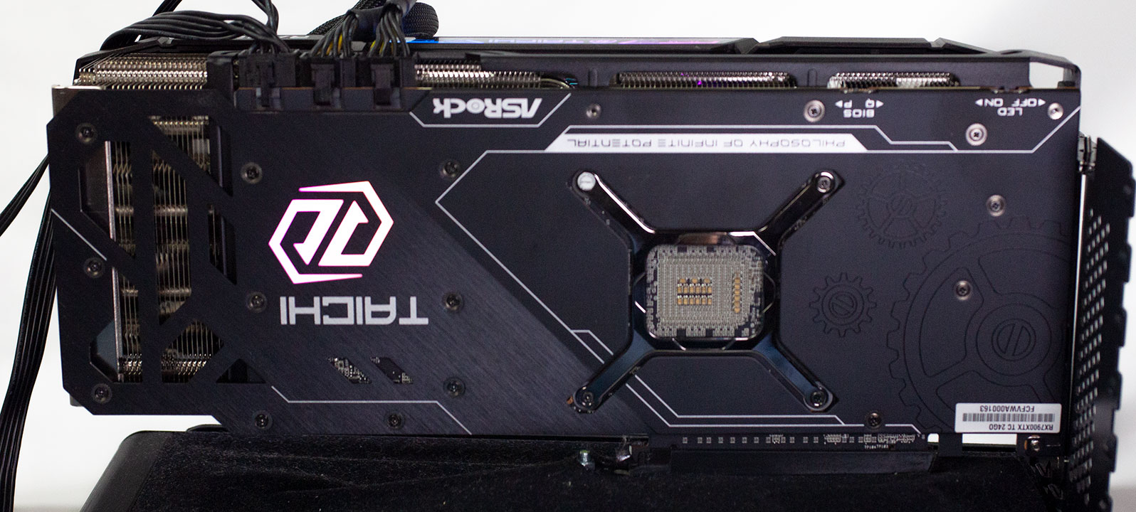
ASRock has placed two RGB zones in the front cooler, one along the top edge, the second near the middle fan. On the back you get a third RGB element that illuminates the Taichi logo.
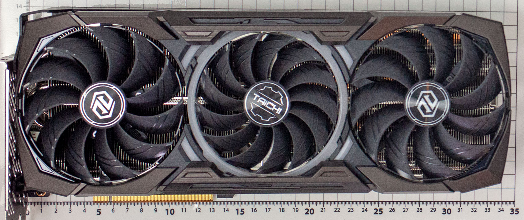
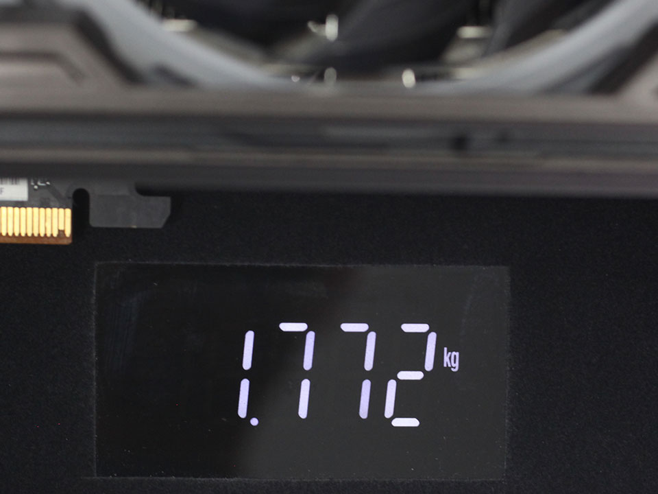
Dimensions of the card are 35.0 x 14.0 cm, and it weighs 1772 g.
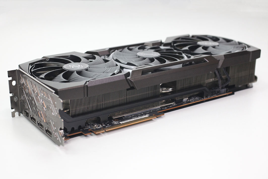
Installation requires three slots in your system.
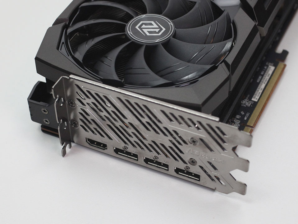
Display connectivity includes two standard DisplayPort 2.1 ports (RDNA 2 had 1.4a) and two HDMI 2.1a (same as RDNA 2).
AMD has upgraded their encode/decode setup. It now comes with two independent hardware units that can encode and decode two streams of video in parallel, or one stream at double the FPS rate. There's support for VP9, H.264, H.265 and AV1 decode, and encoding is supported for H.264, H.265 and AV1.
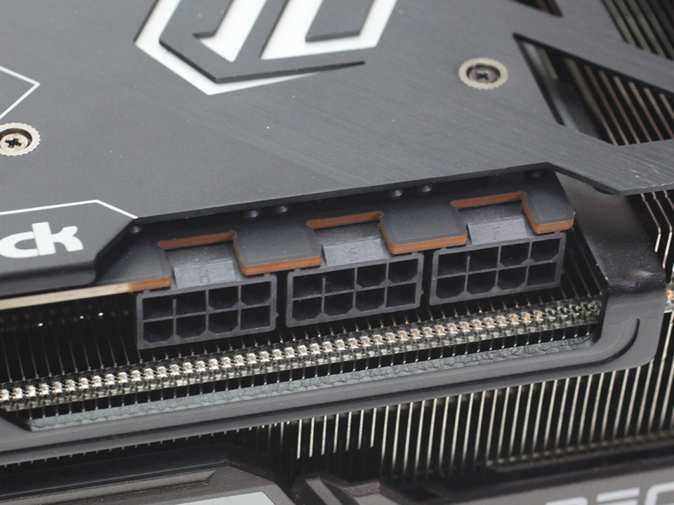
The card uses a classic triple 8-pin power input config, rated for 525 W maximum power. NVIDIA on the other hand uses the new 12+4 pin ATX 12VHPWR connector, which is rated for up to 600 W of power draw.
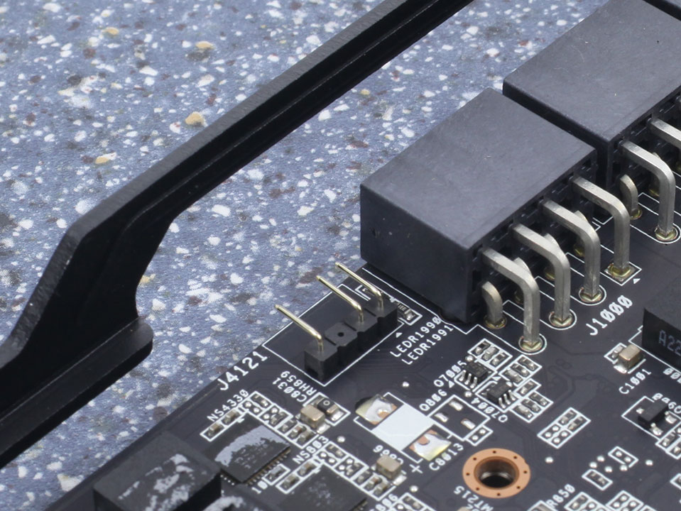
Near the power connectors you'll find a 3-pin ARGB header, which lets you sync the graphics card lighting effects to the rest of your system.
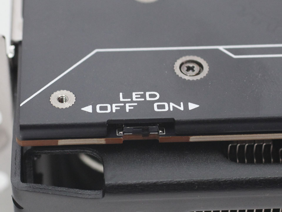
I love this! A dedicated switch lets you turn off the RGB lighting—no software needed.
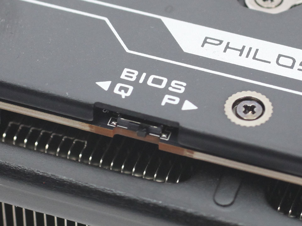
The dual BIOS feature lets you switch between the default "Performance" BIOS and a "Quiet" BIOS. While other vendors reduce the fan speed and allow higher temperatures, ASRock has decided to reduce clocks and voltages instead, which lowers heat output, which makes it easier for the fans to cool the card. This means that both Performance and Quiet mode are running at the same temperatures. Quiet mode is roughly 4% slower, but considerably quieter.
Teardown
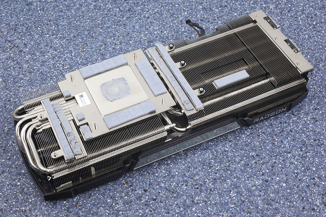
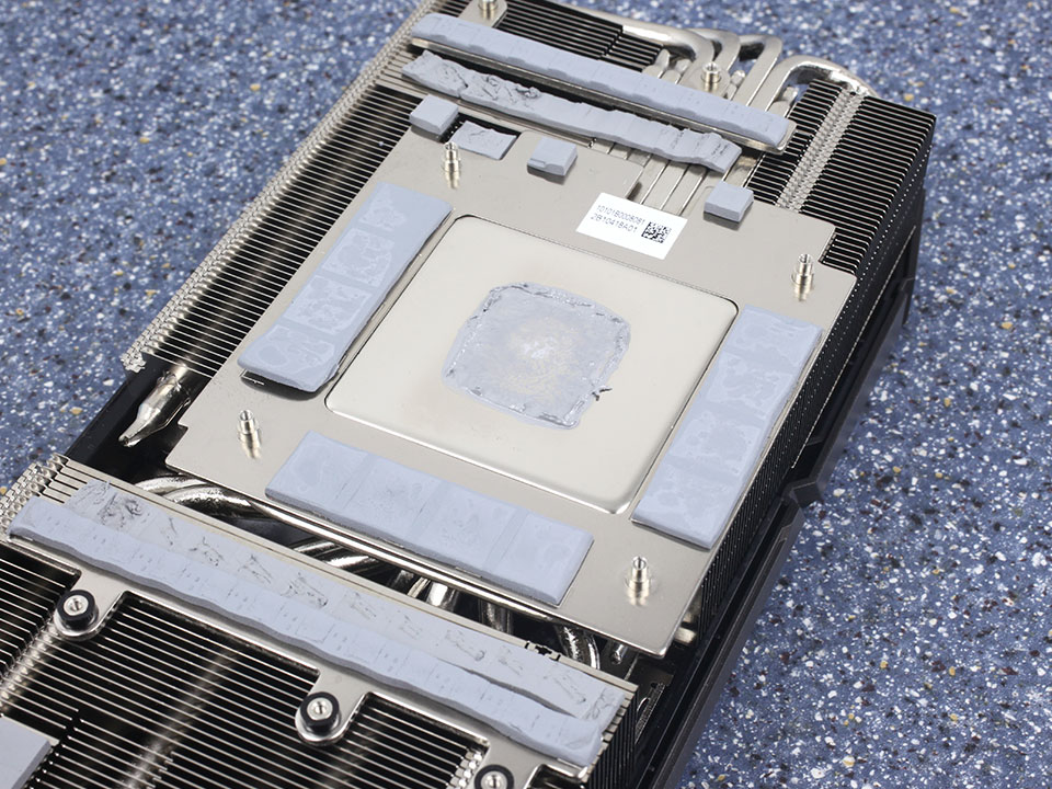
ASRock has engineered an excellent thermal solution that uses eight heatpipes to move heat away quickly from the GPU. The main cooler also provides cooling for the VRM and memory chips.

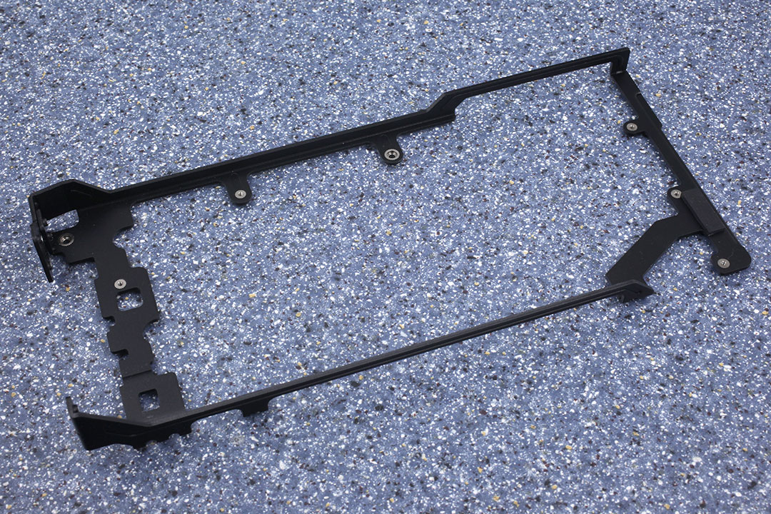
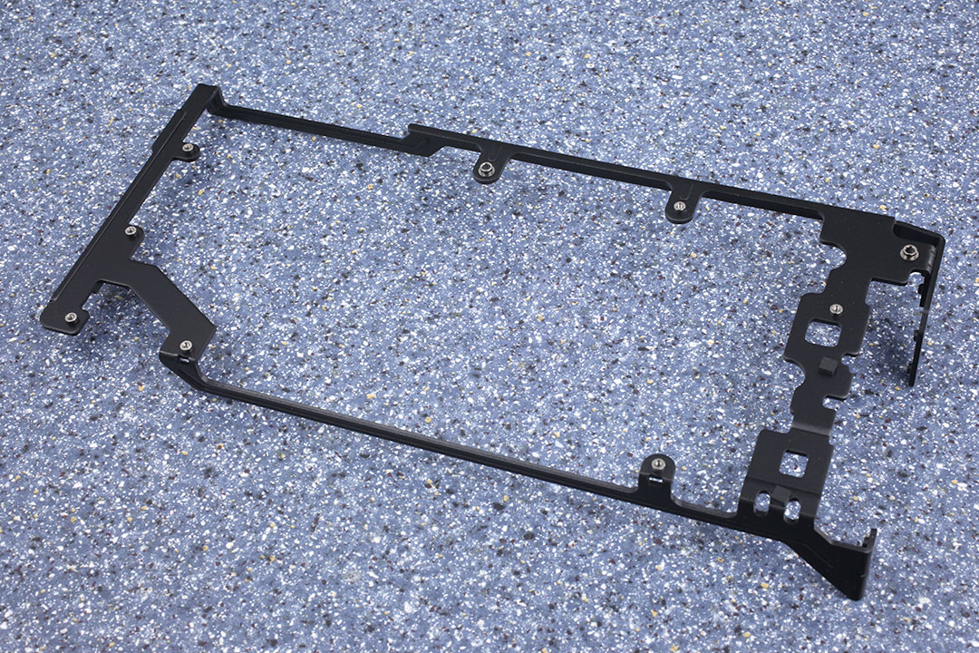
Once the main cooler is removed, a metal reinforcement brace appears, which helps strengthen the card, to protect against warping and sagging.
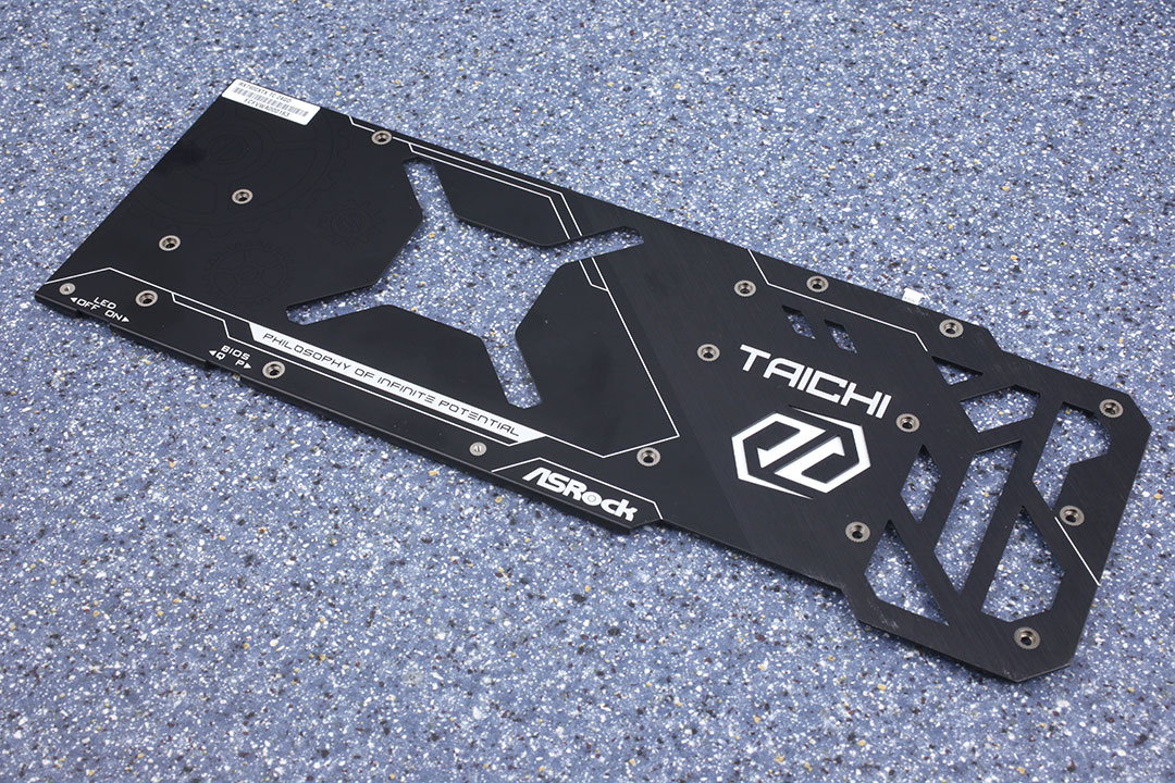

The backplate is made of metal and protects the card against damage during installation and handling.
High-resolution PCB Pictures
These pictures are for the convenience of volt modders and people who would like to see all the finer details on the PCB. Feel free to link back to us and use these in your articles, videos or forum posts.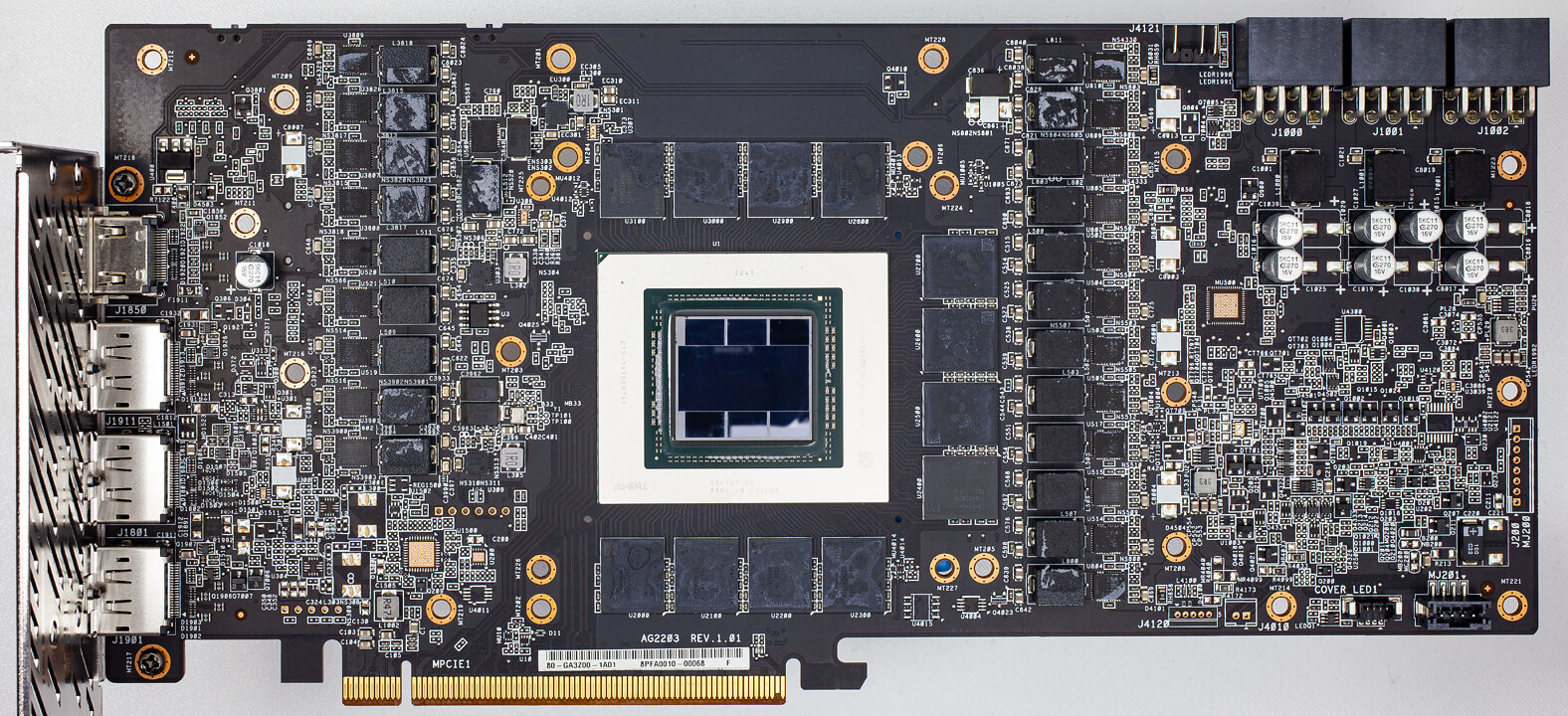

High-resolution versions are also available (front, back).
Circuit Board (PCB) Analysis


GPU voltage is a 18-phase design, managed by a Monolithic Power Systems MP2857 controller.

Monolithic MP87997 DrMOS components are used for GPU voltage; they are rated for 70 A of current each.
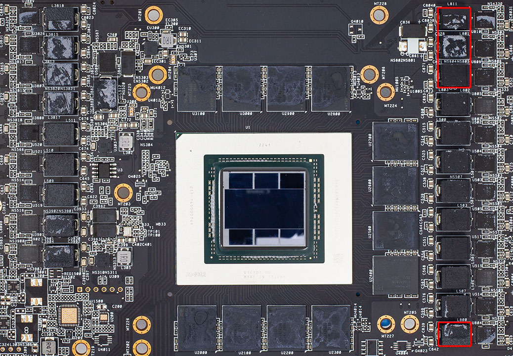

Memory voltage is a four-phase design, managed by a Monolithic Power Systems MP2856 controller.
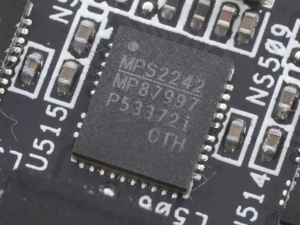
For memory, Monolithic MP87997 DrMOS with a 70 A rating are used again.

The GDDR6 memory chips are made by Hynix and carry the model number H56G42AS8DX-014. They are specified to run at 2500 MHz (20 Gbps effective).

AMD's new Navi 31 graphics processor is the world's first GPU that uses a chiplet architecture. Note the large die in the center, called "GCD," graphics compute die, which houses the compute units, it is surrounded by six smaller "MCD," memory cache dies, that contain one memory controller interface and one slice of cache each. While they look similar, the MCDs are not HBM chips. The MCDs are fabricated on a 6 nm process at TSMC Taiwan with a die size of 36.6 mm² each, the GCD is fabricated using TSMC's 5 nanometer node, with a die size of 300 mm². The combined transistor count of the GPU is 57.7 billion.
Our Patreon Silver Supporters can read articles in single-page format.
Mar 29th, 2025 03:37 EDT
change timezone
Latest GPU Drivers
New Forum Posts
- RX580 BIOS PROBLEM (7)
- What are you playing? (23299)
- Did Nvidia purposely gimp the performance of 50xx series cards with drivers (98)
- How is my CPU's temperature? (21)
- Windows 10 Vs 11, Which one too choose? (116)
- Issues with RTX4090 FE waterblock (Bitspower) (17)
- TechPowerUp Screenshot Thread (MASSIVE 56K WARNING) (4263)
- EVGA 3070ti hotspot is too high 107.7° (4)
- geekbench6 scores (55)
- Will you buy a RTX 5090? (456)
Popular Reviews
- Sapphire Radeon RX 9070 XT Pulse Review
- Samsung 9100 Pro 2 TB Review - The Best Gen 5 SSD
- ASRock Phantom Gaming B850 Riptide Wi-Fi Review - Amazing Price/Performance
- Assassin's Creed Shadows Performance Benchmark Review - 30 GPUs Compared
- be quiet! Pure Rock Pro 3 Black Review
- Sapphire Radeon RX 9070 XT Nitro+ Review - Beating NVIDIA
- ASRock Radeon RX 9070 XT Taichi OC Review - Excellent Cooling
- Palit GeForce RTX 5070 GamingPro OC Review
- Pulsar Feinmann F01 Review
- ASRock Phantom Gaming B860I Lightning Wi-Fi Review
Controversial News Posts
- AMD RDNA 4 and Radeon RX 9070 Series Unveiled: $549 & $599 (260)
- MSI Doesn't Plan Radeon RX 9000 Series GPUs, Skips AMD RDNA 4 Generation Entirely (142)
- Microsoft Introduces Copilot for Gaming (123)
- AMD Radeon RX 9070 XT Reportedly Outperforms RTX 5080 Through Undervolting (118)
- NVIDIA Reportedly Prepares GeForce RTX 5060 and RTX 5060 Ti Unveil Tomorrow (115)
- Over 200,000 Sold Radeon RX 9070 and RX 9070 XT GPUs? AMD Says No Number was Given (100)
- NVIDIA GeForce RTX 5050, RTX 5060, and RTX 5060 Ti Specifications Leak (96)
- Retailers Anticipate Increased Radeon RX 9070 Series Prices, After Initial Shipments of "MSRP" Models (90)