 131
131
ASUS GeForce RTX 3090 STRIX OC Review
Temperatures & Fan Noise »Clock Speeds
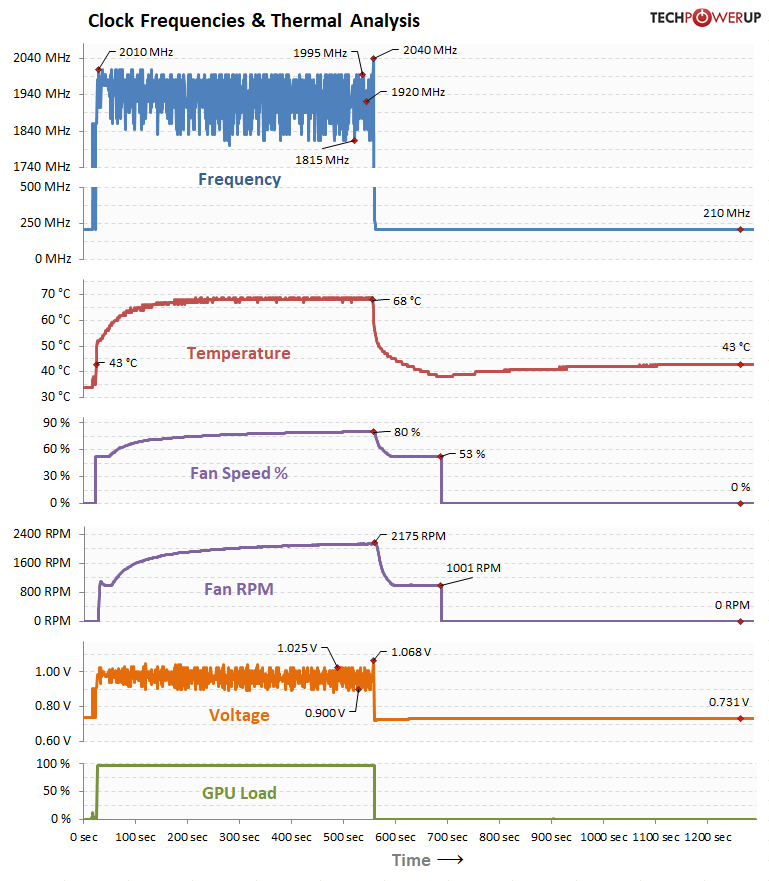
For this test, we first let the card sit in idle to reach thermal equilibrium. Next, we start a constant 100% gaming load, recording several important parameters while the test is running. This shows you the thermal behavior of the card and how the fans ramp up as temperatures increase. Once temperatures are stable (no increase for two minutes), we stop the load and record how the card cools down over time.
We also ran the same test with the "quiet" BIOS:

Another chart with the card manually set to its maximum power limit of 480 W with the default BIOS:

Voltage Frequency Analysis
The card will dynamically adjust clock and voltage based on render load, temperature, and other factors.For the graph below, we recorded all GPU clock and GPU voltage combinations of our 4K UHD resolution benchmarking suite. The plotted points are transparent, which allows them to add up to indicate more often used values. A light color means the clock/voltage combination is rarely used, and a dark color means it's active more often.

Clock Profiles
Modern graphics cards have several clock profiles that are selected to balance power draw and performance requirements.The following table lists the clock settings for important performance scenarios and the GPU voltage that is used in those states.
| GPU Clock | Memory Clock | GPU Voltage | |
|---|---|---|---|
| Desktop | 210 MHz | 51 MHz | 0.737 V |
| Multi-Monitor | 210 MHz | 51 MHz | 0.737 V |
| Media Playback | 210 MHz | 51 MHz | 0.737 V |
| 3D Load | 1545 - 2070 MHz | 1219 MHz | 0.718 - 1.081 V |
Power Limits
All NVIDIA graphics cards have a power limit defined in the BIOS, which limits power draw by adjusting Boost frequencies accordingly. A second limit exists that defines the maximum TDP adjustment limit for user overclocking; i.e., how far the power slider will go. In the second chart, the (+xx%) value lists the percentage increase from the tested card's default power limit to the highest available manual setting—the slider's adjustment range.

Feb 26th, 2025 20:11 EST
change timezone
Latest GPU Drivers
New Forum Posts
- The TPU UK Clubhouse (25809)
- AM3 build, uses in 2025 (12)
- VRR Flicker when using Frame Generation (3)
- TECHPOWERUP HWBOT Contest with Cash Prizes (87)
- TPU's Nostalgic Hardware Club (20012)
- RTX5000 Series Owners Club (138)
- Help with integrated gpu. (62)
- revisiting hpet bcdedit tweaks: what are your timer bench results and settings? (102)
- Testing max ram overclock pn Ryzen 1700 (82)
- Dune: Awakening benchmark - post your results (28)
Popular Reviews
- Corsair Xeneon 34WQHD240-C Review - Pretty In White
- Corsair Virtuoso MAX Wireless Review
- ASUS GeForce RTX 5070 Ti TUF OC Review
- Gigabyte X870 Aorus Elite WiFi 7 Review
- MSI GeForce RTX 5070 Ti Ventus 3X OC Review
- MSI GeForce RTX 5070 Ti Vanguard SOC Review
- Montech HyperFlow Silent 360 Review
- AMD Ryzen 7 9800X3D Review - The Best Gaming Processor
- MSI GeForce RTX 5070 Ti Gaming Trio OC+ Review
- Montech TITAN PLA 1000 W Review
Controversial News Posts
- NVIDIA GeForce RTX 50 Cards Spotted with Missing ROPs, NVIDIA Confirms the Issue, Multiple Vendors Affected (496)
- AMD Radeon 9070 XT Rumored to Outpace RTX 5070 Ti by Almost 15% (304)
- AMD Plans Aggressive Price Competition with Radeon RX 9000 Series (274)
- AMD Radeon RX 9070 and 9070 XT Listed On Amazon - One Buyer Snags a Unit (247)
- NVIDIA Investigates GeForce RTX 50 Series "Blackwell" Black Screen and BSOD Issues (244)
- Edward Snowden Lashes Out at NVIDIA Over GeForce RTX 50 Pricing And Value (241)
- AMD Denies Radeon RX 9070 XT $899 USD Starting Price Point Rumors (239)
- AMD Mentions Sub-$700 Pricing for Radeon RX 9070 GPU Series, Looks Like NV Minus $50 Again (194)