 28
28
ASUS GeForce RTX 5070 TUF OC Review
Test Setup »High-resolution PCB Pictures
These pictures are for the convenience of volt modders and people who would like to see all the finer details on the PCB. Feel free to link back to us and use these in your articles, videos or forum posts.

High-resolution versions are also available (front, back).
Circuit Board (PCB) Analysis
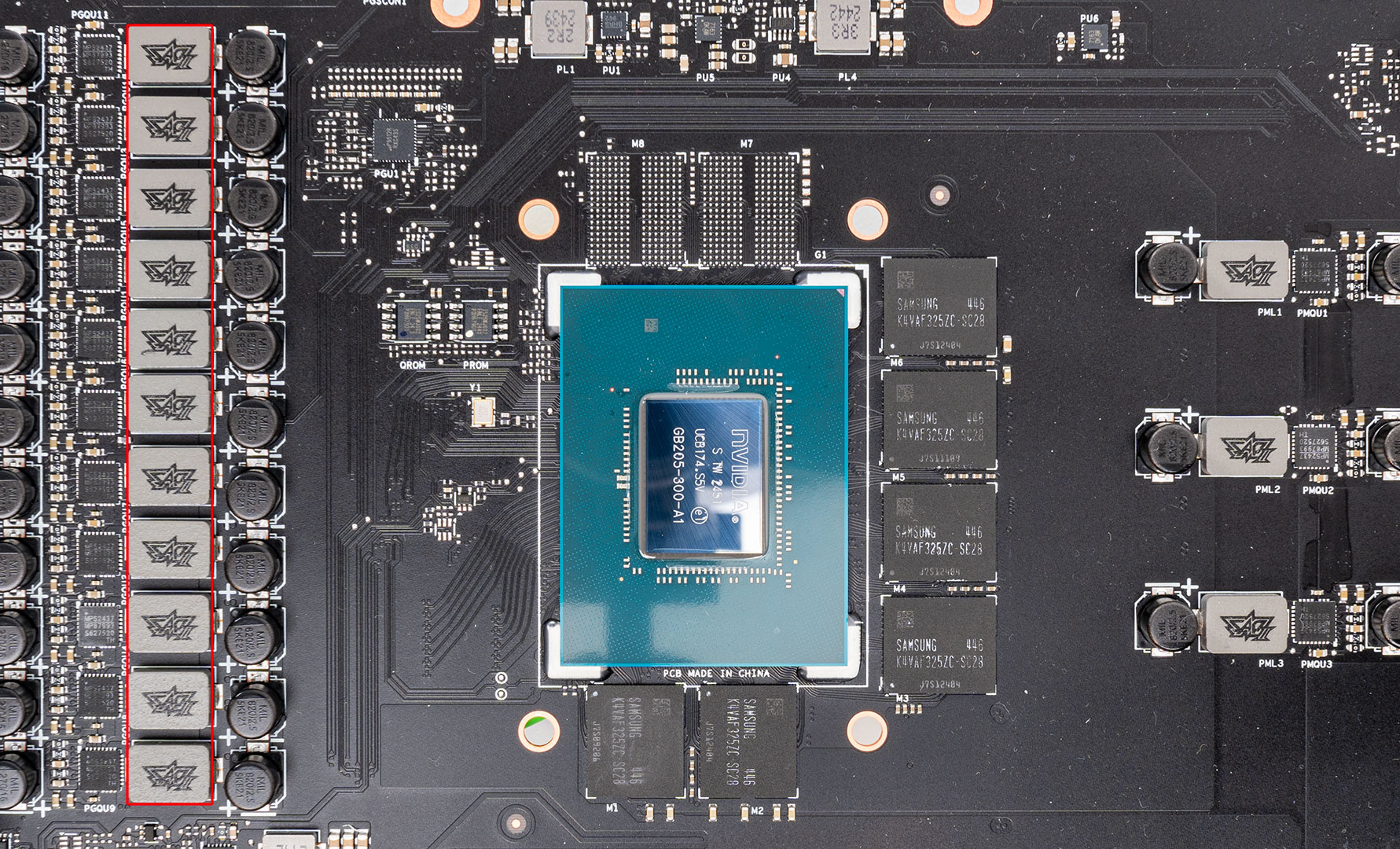
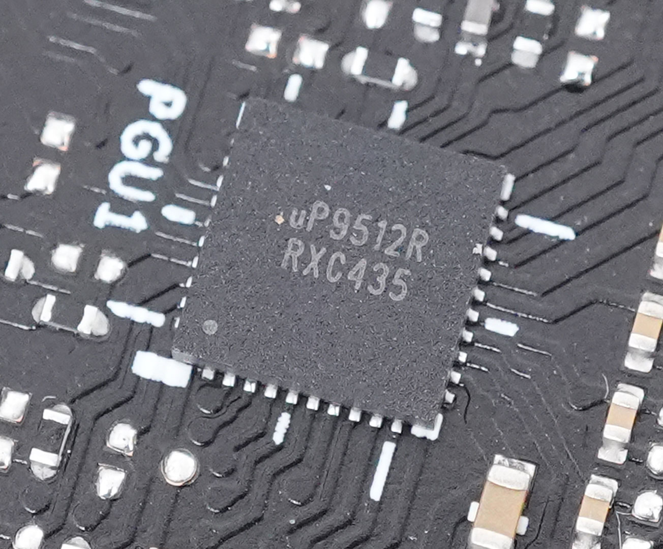
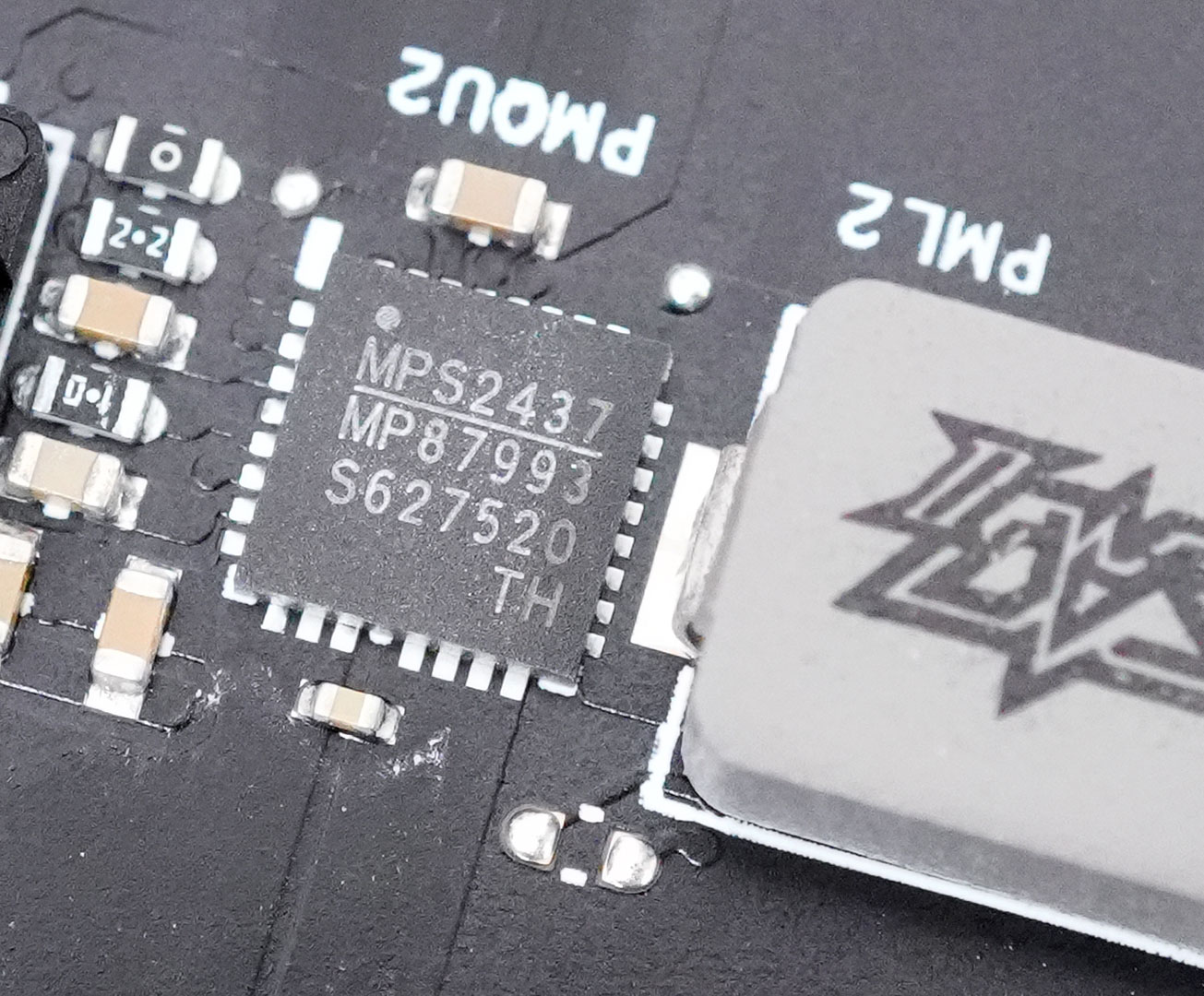
An 11-phase VRM powers the GPU, highlighted in the red rectangles above. These are controlled by a uPI uP9512R voltage controller.
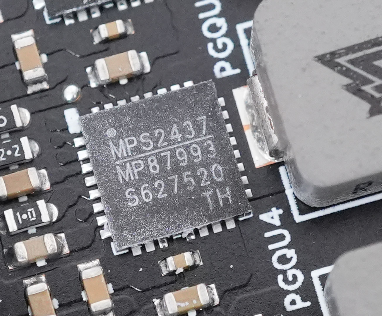
All GPU power phases use Monolithic MPS MP87993 DrMOS with a rating of 50 A.


Powering the six GDDR7 memory chips is a 3-phase VRM driven by a uPI uP9529Q voltage controller.
Just like GPU, the memory is handled by Monolithic MPS MP87993 DrMOS with a rating of 50 A.

The GDDR7 memory chips are made by Samsung, and bear the model number K4VAF325ZC-SC28, they are rated for 28 Gbps.

The NVIDIA GB205 GPU at the heart of the GeForce RTX 5070 is much smaller than the chip used on the RTX 5080 and RTX 5090. It is fabricated using a 5 nanometer "NVIDIA 4N" process at TSMC Taiwan (same process as Ada). The die measures 263 mm², and comes with a transistor count of 31.1 billion.
Mar 25th, 2025 11:01 EDT
change timezone
Latest GPU Drivers
New Forum Posts
- maxsun rx590* vbios (3)
- Is RX 9070 VRAM temperature regular value or hotspot? (188)
- Montech KING 95 - your opinions? (11)
- What local LLM-s you use? (142)
- What's your latest tech purchase? (23391)
- Lenovo ThinkPad L15 Gen 1 (AMD) - DRAM soldered? (8)
- Issues with RTX4090 FE waterblock (Bitspower) (2)
- Is Whatsapp backup broken for anyone else? (1)
- RX 9070 availability (228)
- need help fixing a fake gt730 (1)
Popular Reviews
- Assassin's Creed Shadows Performance Benchmark Review - 30 GPUs Compared
- be quiet! Pure Rock Pro 3 Black Review
- ASUS ProArt X870E-Creator Wi-Fi Review
- ASRock Radeon RX 9070 XT Taichi OC Review - Excellent Cooling
- Sapphire Radeon RX 9070 XT Nitro+ Review - Beating NVIDIA
- ASUS GeForce RTX 5070 TUF OC Review
- AMD Ryzen 9 9950X3D Review - Great for Gaming and Productivity
- Quick Look: Jelly Key Mystic Snake Artisan Keycaps
- AMD Ryzen 7 9800X3D Review - The Best Gaming Processor
- XFX Radeon RX 9070 XT Mercury OC Magnetic Air Review
Controversial News Posts
- AMD RDNA 4 and Radeon RX 9070 Series Unveiled: $549 & $599 (260)
- AMD Mentions Sub-$700 Pricing for Radeon RX 9070 GPU Series, Looks Like NV Minus $50 Again (250)
- AMD Radeon RX 9070-series Pricing Leaks Courtesy of MicroCenter (158)
- MSI Doesn't Plan Radeon RX 9000 Series GPUs, Skips AMD RDNA 4 Generation Entirely (142)
- Microsoft Introduces Copilot for Gaming (123)
- AMD Radeon RX 9070 XT Reportedly Outperforms RTX 5080 Through Undervolting (118)
- NVIDIA Reportedly Prepares GeForce RTX 5060 and RTX 5060 Ti Unveil Tomorrow (115)
- Over 200,000 Sold Radeon RX 9070 and RX 9070 XT GPUs? AMD Says No Number was Given (100)