 128
128
ASUS Radeon RX 7900 XTX TUF OC Review - Amazing Overclocking
(128 Comments) »Introduction
The TUF Gaming Radeon RX 7900 XTX OC is the flagship custom-design RX 7900 XTX graphics card by ASUS, in the apparent-absence of an ROG Strix product. The card features the mammoth 4-slot TUF Gaming cooling solution that the company debuted with its GeForce RTX 4090 TUF Gaming graphics card, and a PCB with increased power delivery from a third 8-pin power connector, to support the factory overclocked speeds. The Radeon RX 7900 XTX is the new flagship from Team Red, with which the company plans to continue competing with NVIDIA in the high-end graphics card segment, and aggressively with pricing. This is thanks to a unique design choice by AMD that keeps Moore's Law alive in spirit if not in letter.
The new Radeon RX 7900 XTX debuts the RDNA 3 graphics architecture, with which the company's is introducing the world's first chiplet-based gaming GPU (a multi-chip module with multiple logic dies). AMD has taken a similar approach with its new GPU as it did with Ryzen processors a few years ago—those components that benefit the most from a switch to a new foundry process are built on them, while specific components that don't need the latest node, are disintegrated and built on separate dies, on a slightly older node. In this case, the Shader Engines, media accelerators, and display controllers, are aggregated into a centralized die called the Graphics Compute Die (GCD) that's built on the latest 5 nm process, while the Infinity Cache memory, memory controllers, and a 64-bit wide GDDR6 memory PHY, are separated into six Memory Cache Dies (MCDs), built on 6 nm. There are six of these on the "Navi 31" GPU powering the RX 7900 XTX, and so it enjoys a 384-bit memory interface. Future Navi 3x series GPUs may feature fewer MCDs to achieve narrower memory interfaces. This way, AMD gets to maximize its foundry allocation of both the 5 nm and 6 nm nodes.

The new RDNA 3 graphics architecture introduces a new compute unit with dual instruction issue-rate SIMD components, support for new math formats, AI acceleration, and 2nd generation Ray Accelerators that improve ray tracing performance over the previous generation. AMD claims a 17.5% IPC uplift over RDNA 2 compute units, which when combined with generationally increased clock-speeds, and a 20% increase in CU counts over "Navi 21," form the bedrock of the performance uplift over the previous generation, with the company claiming to have retained the streak of 50% performance/Watt uplift with each RDNA generation. AMD has also rebalanced its memory system to rely less on the Infinity Cache memory. Each of the six MCDs has a 16 MB segment of the GPU's 96 MB Infinity Cache, which seems less than the 128 MB of the "Navi 21," until you find out that AMD has increased the memory bus width by 50% (256-bit to 384-bit), and is using even faster 20 Gbps memory (compared to 16 Gbps of the RX 6900 XT), which yields a massive 87% memory bandwidth increase.
The most striking aspect of the Radeon RX 7900 series is power, with the top RX 7900 XTX only featuring a 350 W typical board power at reference clocks, compared to the NVIDIA flagship with its 450 W power that can be increased to 600 W or beyond. The reference RX 7900 XTX only features two convenient 8-pin PCIe power connectors, while non-reference cards such as the ASUS TUF Gaming OC in this review, come with three 8-pin connectors for a total of 525 W power delivery capability. GPU clocks have been increased from 2300/2500 MHz on the AMD reference card, to 2395/2565 MHz.
The ASUS official pricing is still unknown. Throughout this review, we've assumed a price point of $1100 and will update everything once official pricing is out.
| Price | Cores | ROPs | Core Clock | Boost Clock | Memory Clock | GPU | Transistors | Memory | |
|---|---|---|---|---|---|---|---|---|---|
| RTX 3070 | $500 | 5888 | 96 | 1500 MHz | 1725 MHz | 1750 MHz | GA104 | 17400M | 8 GB, GDDR6, 256-bit |
| RTX 3070 Ti | $600 | 6144 | 96 | 1575 MHz | 1770 MHz | 1188 MHz | GA104 | 17400M | 8 GB, GDDR6X, 256-bit |
| RX 6800 | $510 | 3840 | 96 | 1815 MHz | 2105 MHz | 2000 MHz | Navi 21 | 26800M | 16 GB, GDDR6, 256-bit |
| RX 6800 XT | $650 | 4608 | 128 | 2015 MHz | 2250 MHz | 2000 MHz | Navi 21 | 26800M | 16 GB, GDDR6, 256-bit |
| RTX 3080 | $750 | 8704 | 96 | 1440 MHz | 1710 MHz | 1188 MHz | GA102 | 28000M | 10 GB, GDDR6X, 320-bit |
| RTX 3080 Ti | $950 | 10240 | 112 | 1365 MHz | 1665 MHz | 1188 MHz | GA102 | 28000M | 12 GB, GDDR6X, 384-bit |
| RX 6900 XT | $700 | 5120 | 128 | 2015 MHz | 2250 MHz | 2000 MHz | Navi 21 | 26800M | 16 GB, GDDR6, 256-bit |
| RX 6950 XT | $800 | 5120 | 128 | 2100 MHz | 2310 MHz | 2250 MHz | Navi 21 | 26800M | 16 GB, GDDR6, 256-bit |
| RTX 3090 | $950 | 10496 | 112 | 1395 MHz | 1695 MHz | 1219 MHz | GA102 | 28000M | 24 GB, GDDR6X, 384-bit |
| RX 7900 XT | $900 | 5376 | 192 | 2000 MHz | 2400 MHz | 2500 MHz | Navi 31 | 57700M | 20 GB, GDDR6, 320-bit |
| RTX 3090 Ti | $1400 | 10752 | 112 | 1560 MHz | 1950 MHz | 1313 MHz | GA102 | 28000M | 24 GB, GDDR6X, 384-bit |
| RTX 4080 | $1200 | 9728 | 112 | 2205 MHz | 2505 MHz | 1400 MHz | AD103 | 45900M | 16 GB, GDDR6X, 256-bit |
| RX 7900 XTX | $1000 | 6144 | 192 | 2300 MHz | 2500 MHz | 2500 MHz | Navi 31 | 57700M | 24 GB, GDDR6, 384-bit |
| ASUS RX 7900 XTX TUF OC | $1100 | 6144 | 192 | 2395 MHz | 2565 MHz | 2500 MHz | Navi 31 | 57700M | 24 GB, GDDR6, 384-bit |
| RTX 4090 | $2400 | 16384 | 176 | 2235 MHz | 2520 MHz | 1313 MHz | AD102 | 76300M | 24 GB, GDDR6X, 384-bit |
AMD RDNA 3 Graphics Architecture
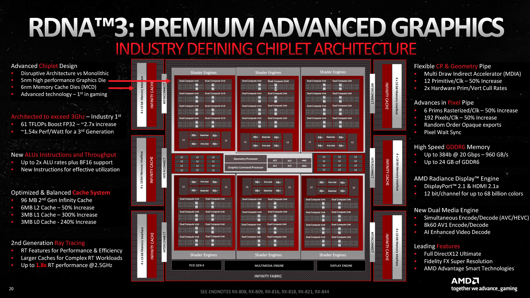
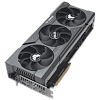
The Radeon RX 7900 XTX and RX 7900 XT debut AMD's 3rd generation RDNA graphics architecture, termed RDNA 3. With it, AMD plans to repeat the generational 50% performance/Watt gain it achieved with RDNA 2, which sprung it back to the high-end graphics segment after a long gap. AMD claims it succeeded in this endeavor, with a 54% generational performance/Watt gain. At the heart of this effort is the switch to the new TSMC 5 nm EUV foundry node. AMD figured out early on that it cannot build large monolithic GPUs on 5 nm without thinning its margins in the fight against NVIDIA, and set out to innovate the Chiplet architecture for the GPU. Under this, specific parts of the GPU that actually benefit from a switch to a newer foundry node, such as the Shader Engines, would be built on a centralized 5 nm die called the Graphics Compute Die (GCD), while those components that can make do with a less advanced node, namely the memory controllers and L3 cache, would be spun off to chiplets called Memory Cache Dies (MCDs), built on 6 nm.


The "Navi 31" GPU is hence a chiplet GPU and not a multi-chip module like "Vega 10." In a chiplet-based device, various components that can otherwise not exist on their own packages, are placed on a single package, with the goal of minimizing production costs, by stratifying their need for a new foundry node, such that only the most power-intensive IP receive the most advanced node. In a MCM, chips that can otherwise exist on their own package, are combined onto a single package for conserving PCB real-estate, or reducing latency. The GCD in the "Navi 31" GPU hence has all the shader engines, caches up to L2, the front-end Command Processor, Async Compute Engines (ACEs), the Display Engine, and the Media Engine. Each of the six MCDs has a 64-bit wide memory bus, and a 16 MB segment of the GPU's 96 MB Infinity Cache memory. The size of the Infinity Cache may have been generationally reduced (compared to 128 MB on "Navi 21"), but AMD has widened the memory bus itself, from 256-bit up to 384-bit.

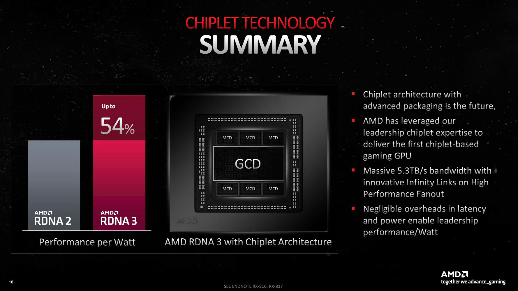
Much of the architectural innovation is not with the chiplet design (a packaging innovation); but at the level of the RDNA 3 Dual-Compute Unit (or Compute Unit pair). The "Navi 31" GPU physically features 96 compute units spread across six Shader Engines. AMD claims that at the same engine clocks, the RDNA 3 CU offers a 17.4% IPC increase over the RDNA 2 CU. There are 20% more CUs over the "Navi 21," and these run at higher engine clocks, tapping into the power headroom afforded by the 5 nm process. These combined work out to the 54% generational performance uplift, with which AMD plans to retain competitiveness with NVIDIA's RTX 40-series "Ada" high-end SKUs.
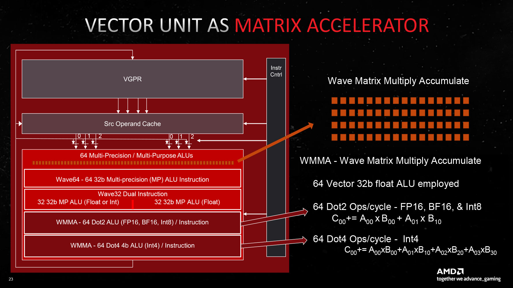
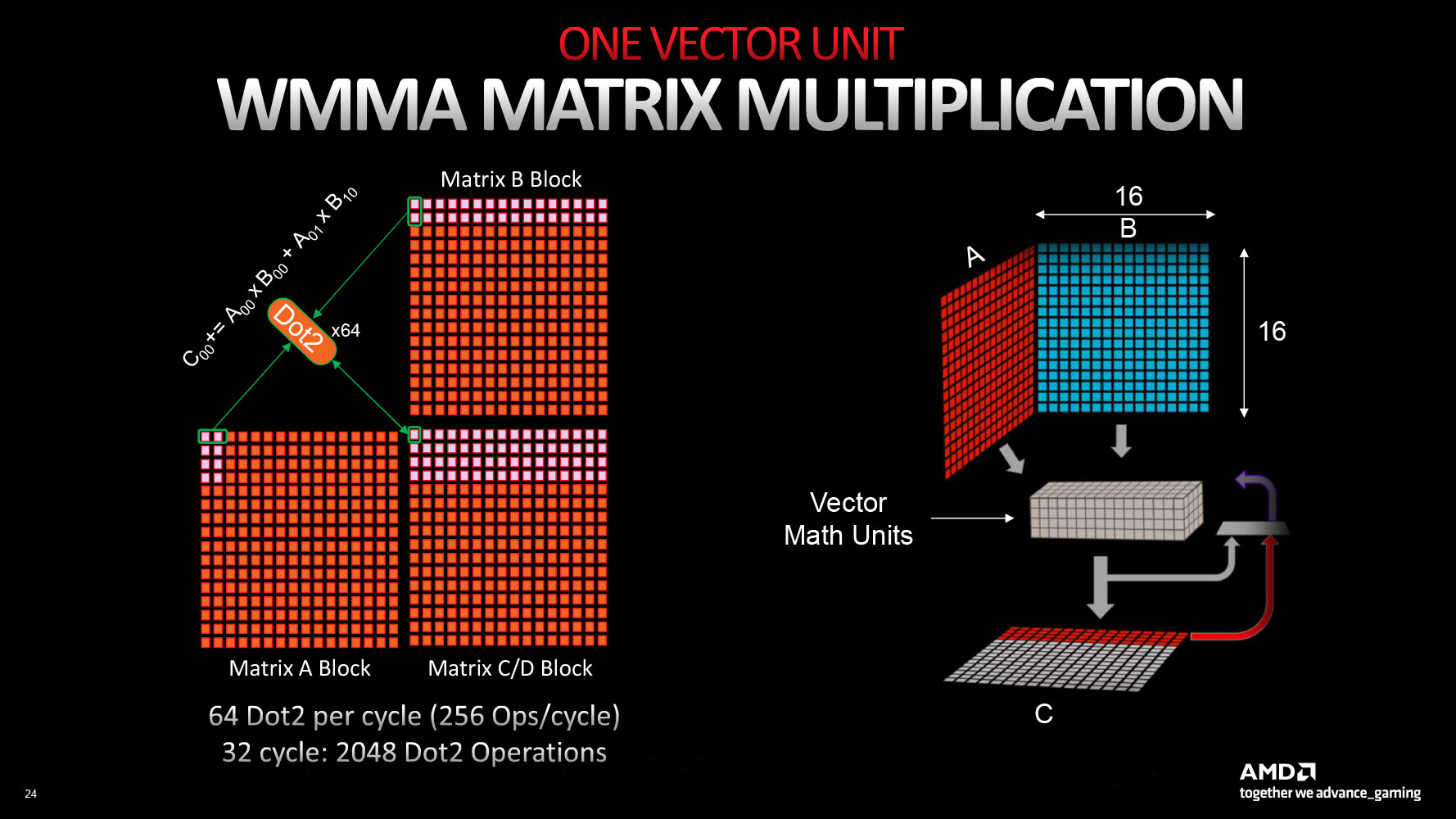
The new RDNA 3 CU introduces multi-precision capability for the 64 stream processors per CU: operating either as 1x SIMD64 or 2x SIMD32 units. The Vector Unit that houses these SIMD units can either function as a SIMD execution mechanism, or as a Matrix execution unit, thanks to the new AI Matrix Accelerator, which provides a 2.7x matrix multiplication performance uplift versus conventional SIMD execution. Also added are support for the Bfloat16 instruction-set, and SIMD8 execution. The GPU hence enjoys AI hardware-acceleration that can be leveraged in future feature-additions relevant to gamers, such as FSR 3.0. Game developers will also look for ways to exploit accelerated AI, now that all three brands feature it (NVIDIA Tensor cores and Intel XMX cores).


AMD's first-generation Ray Accelerator, introduced with the RDNA 2 architecture, was the result of a hasty effort to catch up to NVIDIA with a DirectX 12 Ultimate GPU, where they developed a fixed-function hardware to calculate ray intersections, and offloaded a large chunk of RT processing to the generationally-doubled SIMD resources. With RDNA 3, they've refined the Ray Accelerator to achieve an 80% ray tracing performance uplift over the previous generation, when you add up the Ray Accelerator count, their higher engine clocks, and other hardware-level optimizations, such as early sub-tree culling, specialized box sorting modes, and reduced traversal iterations.


There is a 50% ray intersection capacity improvement for the "Navi 31" GPU thanks to these optimizations, and cycles-per-ray reduction. Besides these, AMD has also made several improvements to the geometry- and pixel-pipes, with the introduction of the new multi-draw indirect accelerator (MDIA), which reduces CPU API and driver-level overheads by gathering and parsing multi-draw command data. At the hardware-level 12 primitives per clock is now supported compared to 8 per clock on RDNA 2, thanks to culling. The core-configuration overall enables 50% more rasterized performance per clock.
The GCD features six Shader Engines, each with 16 compute units (or 8 dual compute units), which work out to 1,024 stream processors. Six such Shader Engines make up 6,144 stream processors with 96 Ray Accelerators and 96 AI Accelerators. The GPU has 384 TMUs, and a massive 192 ROPs—a 50% increase over "Navi 21." The Radeon RX 7900 XTX enables all 96 CUs, and maxes out the silicon, whereas the RX 7900 XT has 84 out of 96 CUs enabled, which work out to 5,376 stream processors, 84 Ray Accelerators, 336 TMUs, and an unchanged 192 ROPs. The RX 7900 XTX gets 24 GB of GDDR6 memory across the GPU's entire 384-bit memory bus, with a memory speed of 20 Gbps (GDDR6-effective), translating to 960 GB/s of memory bandwidth. The RX 7900 XT is equipped with 20 GB of memory across a narrower 320-bit memory bus carved out by disabling one of the six MCDs. At the same 20 Gbps speed, this yields 800 GB/s bandwidth.
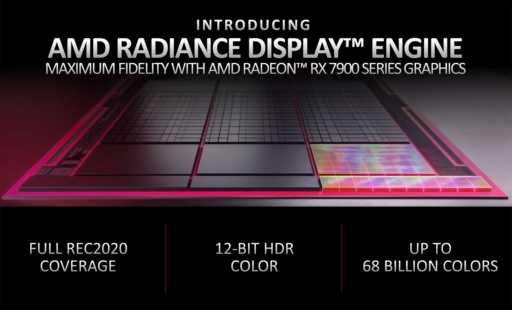

AMD has significantly improved the Display Engine of "Navi 31" over the previous-generation in terms of connectivity. The new Radiance Display Engine comes with native support for DisplayPort 2.1, which enables 8K output at up to 165 Hz refresh-rate, or 4K at up to 480 Hz, with a single cable. AMD has refined its FSR 2 algorithm to support 8K (i.e. render at a lower resolution with FSR-enhanced upscaling), to make it possible to enjoy the latest AAA titles at playable frame-rates on 8K displays. Both the RX 7900 series cards get two full-size DP 2.1 connectors, besides an HDMI 2.1b, and a USB-C with DP 1.2 passthrough. The "Navi 31" silicon receives full hardware-accelerated AV1 encode and decode capabilities, through dual independent encode/decoders, so two independent video streams can be simultaneously transcoded, or one stream at twice the framerate. With this generation, AMD is also introducing SmartAccess Video, a feature that lets the AMD driver leverage the hardware encoders of the RDNA 2 iGPU of Ryzen 7000 desktop processors, for additional encoding performance.
Packaging


The Card

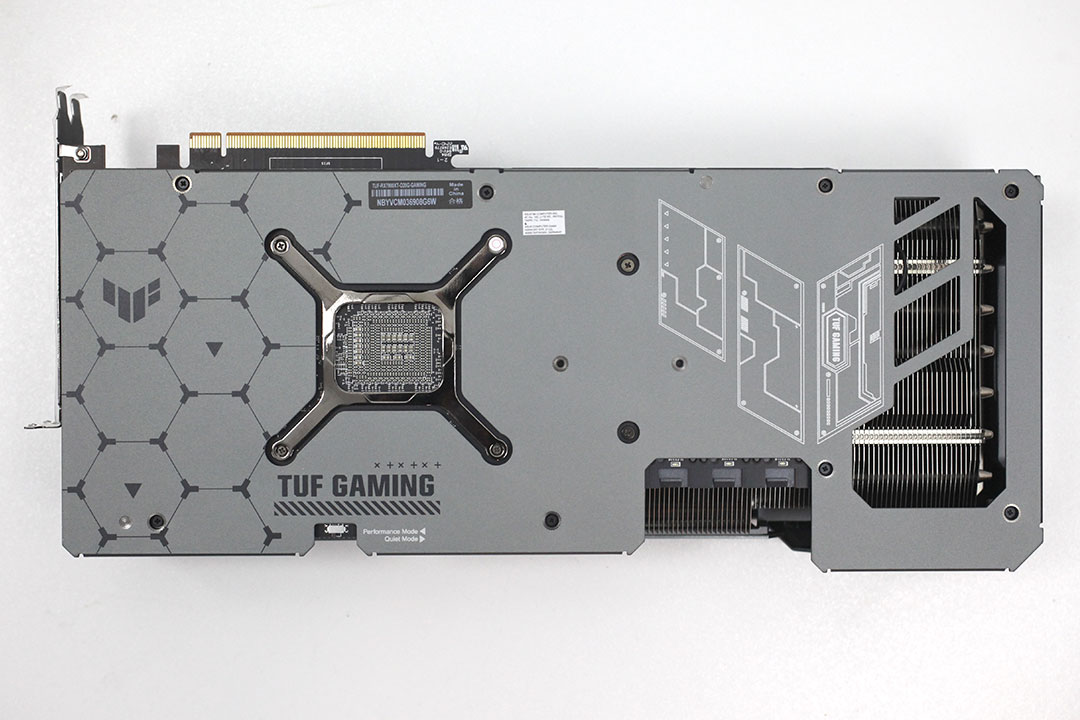
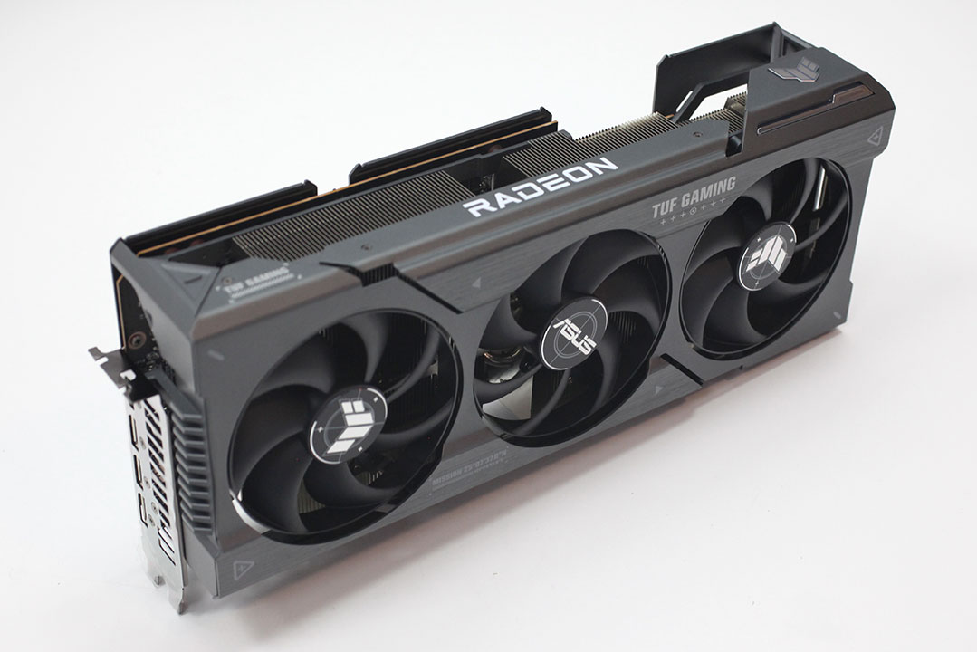
ASUS is reusing the same design philosophy that we've seen on the company's RTX 4090/4080 TUF. The main color theme is gray and black with metallic highlights. I have to say I really like the sleek looks of the card, and the matte metal surface. Both the main cooler shroud and backplate are made from thick metal.


Dimensions of the card are 35.5 x 18.05 cm, and it weighs 2135 g.

Installation requires four slots in your system.

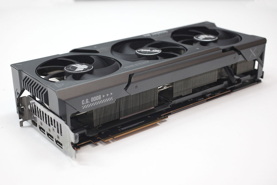
Display connectivity includes three standard DisplayPort 2.1 ports (RDNA 2 had 1.4a) and one HDMI 2.1a (same as RDNA 2).
AMD has upgraded their encode/decode setup. It now comes with two independent hardware units that can encode and decode two streams of video in parallel, or one stream at double the FPS rate. There's support for VP9, H.264, H.265 and AV1 decode, and encoding is supported for H.264, H.265 and AV1.
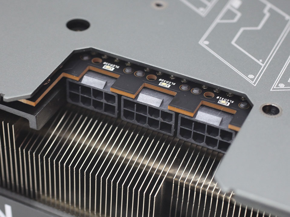
The card uses a classic triple 8-pin power input config, rated for 525 W maximum power. NVIDIA on the other hand uses the new 12+4 pin ATX 12VHPWR connector, which is rated for up to 600 W of power draw.

This dual BIOS switch lets you toggle between the default "performance" BIOS and a "quiet" BIOS, which runs the fans at slower speed.
Teardown


The main heatsink provides cooling for the GPU chip, memory chips and VRM circuitry. Unlike most Radeon RX 7900 Series designs, the baseplate is not a vapor-chamber design. Seven heatpipes move heat away from the GPU surface to the cooling fins.


The backplate is made from thick metal and of excellent build quality. It protects the card against damage during installation and handling.
High-resolution PCB Pictures
These pictures are for the convenience of volt modders and people who would like to see all the finer details on the PCB. Feel free to link back to us and use these in your articles, videos or forum posts.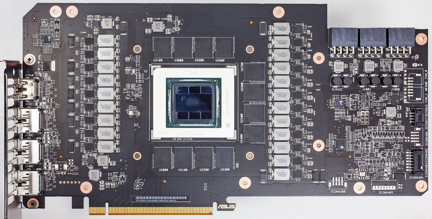

High-resolution versions are also available (front, back).
Our Patreon Silver Supporters can read articles in single-page format.
Mar 28th, 2025 08:03 EDT
change timezone
Latest GPU Drivers
New Forum Posts
- Will you buy a RTX 5090? (455)
- Technical Issues - TPU Main Site & Forum (2025) (81)
- Should you physically remove secondary NVMe drives when performing a clean Windows install? (40)
- AMD RX 9070 XT & RX 9070 non-XT thread (OC, undervolt, benchmarks, ...) (64)
- Future-proofing my OLED (33)
- RTX 3050 with GA107 GPU incomplete information and sensor issue. (0)
- Post your Monster Hunter Wilds benchmark scores (151)
- Compatibility With Alphacool Core RX 9070 XT Taichi GPU WaterBlock ?? (0)
- Recommended PhysX card for 5xxx series? [Is vRAM relevant?] (226)
- Is RX 9070 VRAM temperature regular value or hotspot? (247)
Popular Reviews
- Sapphire Radeon RX 9070 XT Pulse Review
- Samsung 9100 Pro 2 TB Review - The Best Gen 5 SSD
- Assassin's Creed Shadows Performance Benchmark Review - 30 GPUs Compared
- Pulsar Feinmann F01 Review
- ASRock Phantom Gaming B860I Lightning Wi-Fi Review
- be quiet! Pure Rock Pro 3 Black Review
- Sapphire Radeon RX 9070 XT Nitro+ Review - Beating NVIDIA
- ASRock Radeon RX 9070 XT Taichi OC Review - Excellent Cooling
- AMD Ryzen 7 9800X3D Review - The Best Gaming Processor
- ASUS ProArt X870E-Creator Wi-Fi Review
Controversial News Posts
- AMD RDNA 4 and Radeon RX 9070 Series Unveiled: $549 & $599 (260)
- MSI Doesn't Plan Radeon RX 9000 Series GPUs, Skips AMD RDNA 4 Generation Entirely (142)
- Microsoft Introduces Copilot for Gaming (123)
- AMD Radeon RX 9070 XT Reportedly Outperforms RTX 5080 Through Undervolting (118)
- NVIDIA Reportedly Prepares GeForce RTX 5060 and RTX 5060 Ti Unveil Tomorrow (115)
- Over 200,000 Sold Radeon RX 9070 and RX 9070 XT GPUs? AMD Says No Number was Given (100)
- NVIDIA GeForce RTX 5050, RTX 5060, and RTX 5060 Ti Specifications Leak (96)
- Retailers Anticipate Increased Radeon RX 9070 Series Prices, After Initial Shipments of "MSRP" Models (90)