 19
19
Gigabyte Radeon RX 6900 XT Gaming OC Review
Test Setup »High-resolution PCB Pictures
These pictures are for the convenience of volt modders and people who would like to see all the finer details on the PCB. Feel free to link back to us and use these in your articles or forum posts.

High-res versions are also available (front, back).
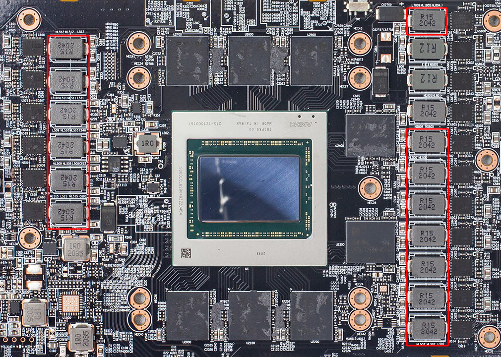
Circuit Board (PCB) Analysis
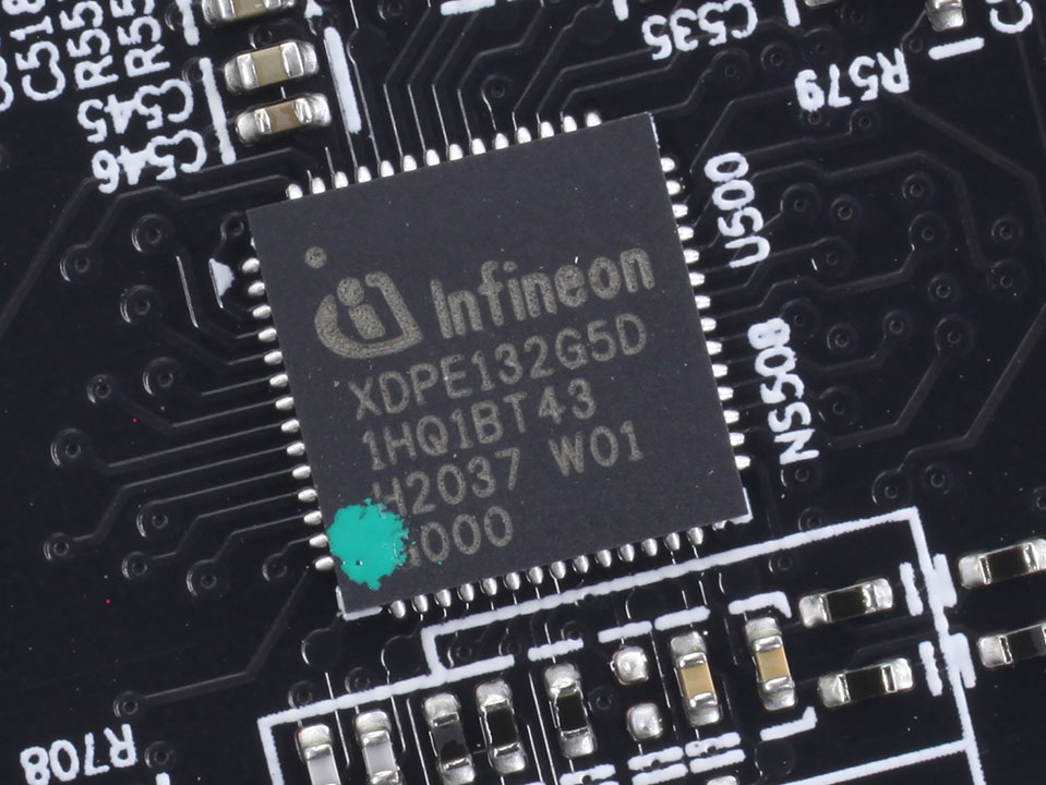
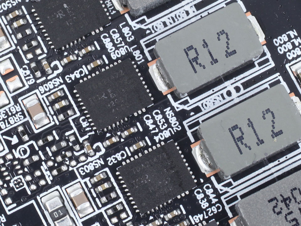
GPU voltage is powered by the expensive Infineon XDPE132G5D running 14 power phases.
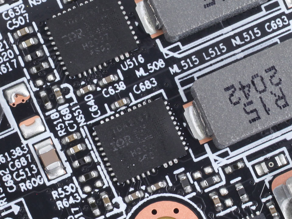
International Rectifier TDA21472 DrMOS chips are used for GPU voltage.
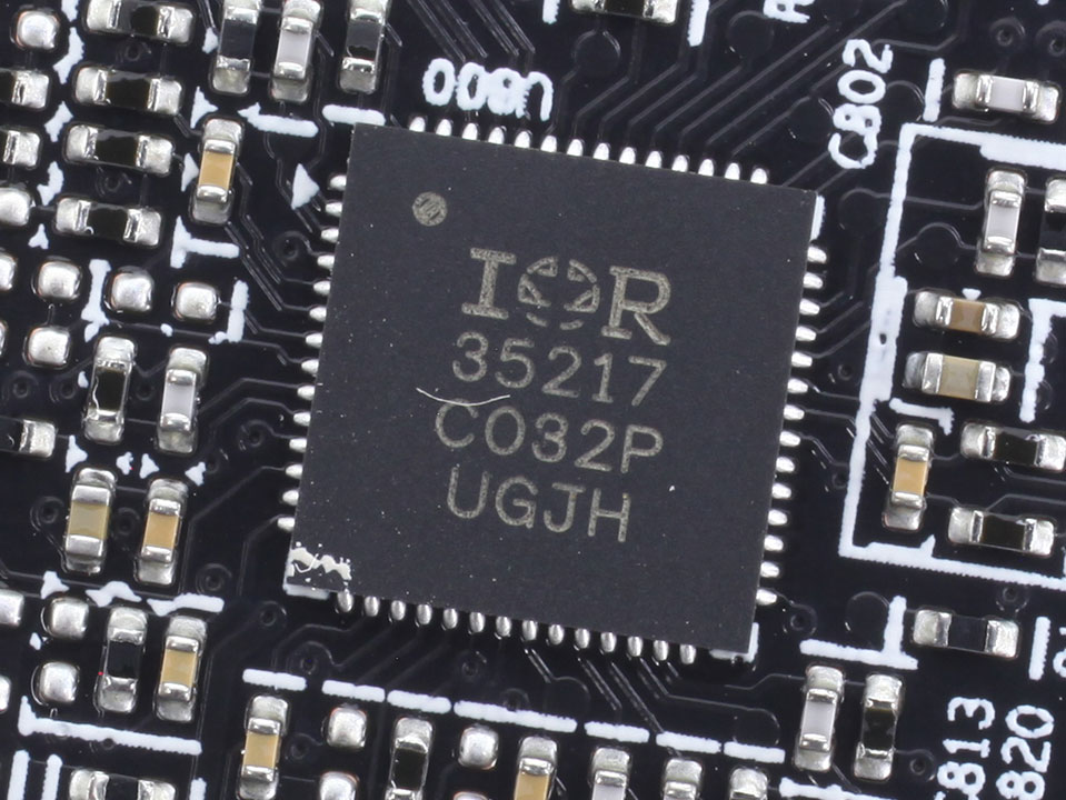
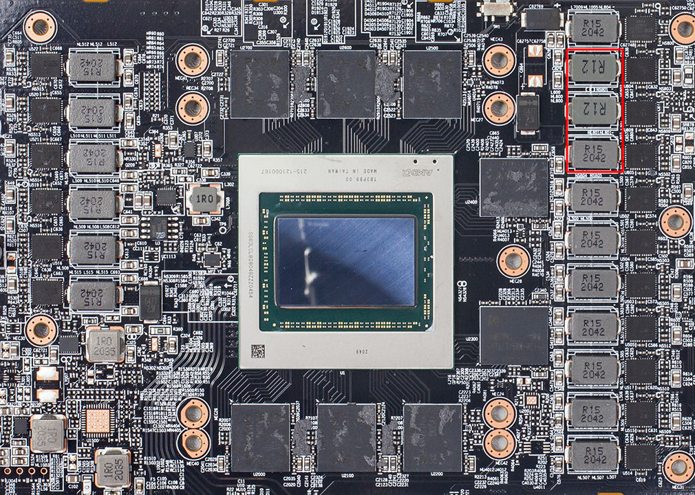
Memory voltage uses a three-phase design and is generated by an IRF35217 controller.
For memory, TDA21472 DrMOS chips are used, too.

The GDDR6 chips are made by Samsung, carry the model number "K4ZAF325BM-HC16," and are rated to run at 16 Gbps.
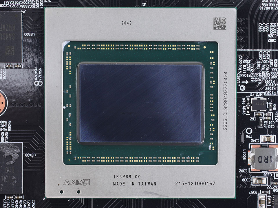
Built on the same TSMC N7 (7 nm) node as Navi 10, the Navi 21 silicon is spread across a 519.8 mm² die area and packs 26.8 billion transistors. The pinkish-red tinge we saw on Navi 10 is gone.
Mar 4th, 2025 00:03 EST
change timezone
Latest GPU Drivers
New Forum Posts
- The future of RDNA on Desktop. (17)
- GameTechBench GPU benchmark is already out! (292)
- Found a weird Radeon HD 7950 with 1536 shaders and no temperature readout (27)
- Cooling problems persist on LGA1700 (25)
- Cryptocoin Value and Market Trend Discussion (1613)
- It's happening again, melting 12v high pwr connectors (993)
- *Severe micro stutters* cyberpunk 2077 Please help (16)
- Easy to open wired mice (0)
- Was pentium 4 an over engineered CPU? (93)
- Will you buy a RTX 5090? (425)
Popular Reviews
- AMD Radeon RX 9070 Series Technical Deep Dive
- ASUS GeForce RTX 5070 Ti TUF OC Review
- be quiet! Pure Base 501 DX Review
- AMD Ryzen 7 9800X3D Review - The Best Gaming Processor
- MSI GeForce RTX 5070 Ti Vanguard SOC Review
- RAWM ES21M Review
- ASUS ROG Harpe Ace Mini Review
- MSI GeForce RTX 5070 Ti Ventus 3X OC Review
- EIZO FlexScan EV4340X Review - A Multitasking Powerhouse
- Gigabyte X870 Aorus Elite WiFi 7 Review
Controversial News Posts
- NVIDIA GeForce RTX 50 Cards Spotted with Missing ROPs, NVIDIA Confirms the Issue, Multiple Vendors Affected (513)
- AMD Plans Aggressive Price Competition with Radeon RX 9000 Series (274)
- AMD Radeon RX 9070 and 9070 XT Listed On Amazon - One Buyer Snags a Unit (260)
- AMD Mentions Sub-$700 Pricing for Radeon RX 9070 GPU Series, Looks Like NV Minus $50 Again (248)
- NVIDIA Investigates GeForce RTX 50 Series "Blackwell" Black Screen and BSOD Issues (244)
- AMD RDNA 4 and Radeon RX 9070 Series Unveiled: $549 & $599 (229)
- AMD Radeon RX 9070 and 9070 XT Official Performance Metrics Leaked, +42% 4K Performance Over Radeon RX 7900 GRE (195)
- AMD Radeon RX 9070-series Pricing Leaks Courtesy of MicroCenter (158)