 89
89
Intel Core i5-12600 Review - To E or not to E
(89 Comments) »Introduction
The Core i5-12600 "Alder Lake" forms the leader of a sub-series of 12th Gen Core i5 processors. While usually non-K, K and KF-variants are quite similar as the only difference is integrated graphics or overclocking. The Core i5-12600 is a very different processor from the Core i5-12600K and i5-12600KF, though. Actually, the i5-12600 in this review has more in common with the very tempting i5-12400F we recently reviewed. With its 12th Generation, Intel branched its Core i5 desktop processor series out into two sub-series. The i5-12600K and KF are based on the larger Alder Lake C0 die and offer the Hybrid architecture, which has six performance "P-cores" working next to four efficiency "E-cores." The rest of the Core i5 series is based on a physically smaller die codenamed "H0," which only has six P-cores and no E-cores. The i5-12600 we are reviewing today is the fastest of these H0 processors you can buy. This also makes it the fastest Alder Lake processor without E-cores.

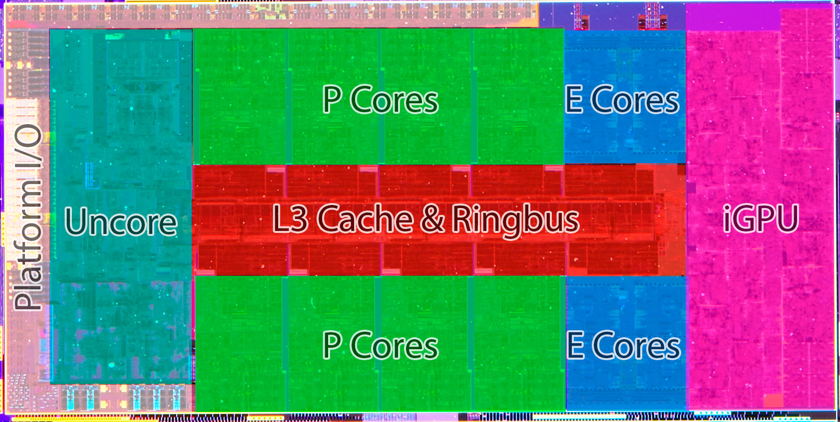
The Core i5-12600 is a traditional multi-core processor with none of the Hybrid processing elements found in the i5-12600K. It is a 6-core/12-thread processor with six "Golden Cove" performance cores and no "Gracemont" E-core clusters on the silicon. Each of these P-cores has 1.25 MB of dedicated L2 cache, and the six cores share an 18 MB L3 cache. The iGPU, uncore, and platform I/O is identical to the other Core Alder Lake processors, including support for DDR5 memory and PCI-Express Gen 5.
The Core i5 H0 series includes the i5-12400/F, i5-12500, and this chip, the i5-12600. The Core i3 quad-core models are carved out of this exact silicon by disabling two cores. The i5-12600 ticks at a base frequency of 3.30 GHz, with 4.80 GHz maximum Turbo Boost frequency. Its power limits are identical to those of the i5-12400 with 65 W processor base power and 117 W maximum turbo power. The UHD Graphics 770 iGPU is based on the Xe LP graphics architecture and sees 32 EUs (256 programmable shaders) run at up to 1.45 GHz graphics clock.
Intel is offering the Core i5-12600 at around $240, which makes it $30 cheaper than the i5-12600K and just $20 cheaper than the i5-12600KF that comes with a disabled iGPU. As we mentioned earlier, you have to be very careful when ordering these chips as a misplaced "K" can land you with a significantly different chip. In this review, we find out if it's worth considering the E-core-free Core i5-12600 over its cousins with E-cores that promise you more compute muscle for just an additional $20-30.
| Price | Cores / Threads | Base Clock | Max. Boost | L3 Cache | TDP | Architecture | Process | Socket | |
|---|---|---|---|---|---|---|---|---|---|
| Core i5-9400F | $165 | 6 / 6 | 2.9 GHz | 4.1 GHz | 9 MB | 65 W | Coffee Lake | 14 nm | LGA 1151 |
| Core i5-10400F | $125 | 6 / 12 | 2.9 GHz | 4.3 GHz | 12 MB | 65 W | Comet Lake | 14 nm | LGA 1200 |
| Core i5-11400F | $160 | 6 / 12 | 2.6 GHz | 4.4 GHz | 12 MB | 65 W | Rocket Lake | 14 nm | LGA 1200 |
| Core i5-12400F | $180 | 6 / 12 | 2.5 GHz | 4.4 GHz | 18 MB | 65 W | Alder Lake | 10 nm | LGA 1700 |
| Core i5-10500 | $205 | 6 / 12 | 3.1 GHz | 4.5 GHz | 12 MB | 65 W | Comet Lake | 14 nm | LGA 1200 |
| Ryzen 5 3600 | $230 | 6 / 12 | 3.6 GHz | 4.2 GHz | 32 MB | 65 W | Zen 2 | 7 nm | AM4 |
| Core i5-9600K | $220 | 6 / 6 | 3.7 GHz | 4.6 GHz | 9 MB | 95 W | Coffee Lake | 14 nm | LGA 1151 |
| Core i5-10600K | $210 | 6 / 12 | 4.1 GHz | 4.8 GHz | 12 MB | 125 W | Comet Lake | 14 nm | LGA 1200 |
| Core i5-11600K | $210 | 6 / 12 | 3.9 GHz | 4.9 GHz | 12 MB | 125 W | Rocket Lake | 14 nm | LGA 1200 |
| Ryzen 5 3600X | $190 | 6 / 12 | 3.8 GHz | 4.4 GHz | 32 MB | 95 W | Zen 2 | 7 nm | AM4 |
| Ryzen 5 5600G | $225 | 6 / 12 | 3.9 GHz | 4.4 GHz | 16 MB | 65 W | Zen 3 + Vega | 7 nm | AM4 |
| Ryzen 5 5600X | $230 | 6 / 12 | 3.7 GHz | 4.6 GHz | 32 MB | 65 W | Zen 3 | 7 nm | AM4 |
| Core i5-12600 | $240 | 6 / 12 | 3.3 GHz | 4.8 GHz | 18 MB | 65 W | Alder Lake | 10 nm | LGA 1700 |
| Core i5-12600K | $270 | 6+4 / 16 | 3.7 / 2.8 GHz | 4.9 / 3.6 GHz | 20 MB | 125 W | Alder Lake | 10 nm | LGA 1700 |
| Core i7-9700K | $310 | 8 / 8 | 3.6 GHz | 4.9 GHz | 12 MB | 95 W | Coffee Lake | 14 nm | LGA 1151 |
| Core i7-10700K | $325 | 8 / 16 | 3.8 GHz | 5.1 GHz | 16 MB | 125 W | Comet Lake | 14 nm | LGA 1200 |
| Core i7-11700K | $315 | 8 / 16 | 3.6 GHz | 5.0 GHz | 16 MB | 125 W | Rocket Lake | 14 nm | LGA 1200 |
| Ryzen 7 3700X | $320 | 8 / 16 | 3.6 GHz | 4.4 GHz | 32 MB | 65 W | Zen 2 | 7 nm | AM4 |
| Ryzen 7 5700G | $350 | 8 / 16 | 3.8 GHz | 4.6 GHz | 16 MB | 65 W | Zen 3 + Vega | 7 nm | AM4 |
| Core i7-12700K | $385 | 8+4 / 20 | 3.6 / 2.7 GHz | 5.0 / 3.8 GHz | 25 MB | 125 W | Alder Lake | 10 nm | LGA 1700 |
| Ryzen 7 5800X | $350 | 8 / 16 | 3.8 GHz | 4.7 GHz | 32 MB | 105 W | Zen 3 | 7 nm | AM4 |

Intel paper-launched the 12th Gen Core processor family on October 27, allowing us to post everything about the processor except performance testing, so we did a more comprehensive preview article on the Alder Lake microarchitecture. The Core i5-12600 is based on a physically smaller die than the C0 die of the i9-12900K, codenamed "H0." There are no die shots from Intel of this die, but MSI OC Lab de-lidded a Core i5 H0 processor and compared its die size with that of the larger die. Built on the same Intel 7 node as the C0 die, formerly known as 10 nm Enhanced SuperFin, the new H0 die is about 24% smaller in area. Considering these are high-volume SKUs, that's massive savings in wafer consumption at scale.
Unlike the C0 die, which physically features 8 Golden Cove P-cores and 8 Gracemont E-cores, the H0 silicon lacks E-cores and physically only has 6 "Golden Cove" P-cores. With the E-core clusters and a couple of P-cores out of the way, the shared L3 cache size is proportionately reduced to 18 MB. The uncore (integrated northbridge), Xe-LP graphics core and I/O interfaces are the same as on the C0 die. You get 16 lanes of PCI-Express Gen 5 which go toward the PEG slot, 4 lanes of PCI-Express Gen 4 toward a CPU-attached M.2 NVMe slot, and 8 DMI Gen4 lanes toward the chipset bus.
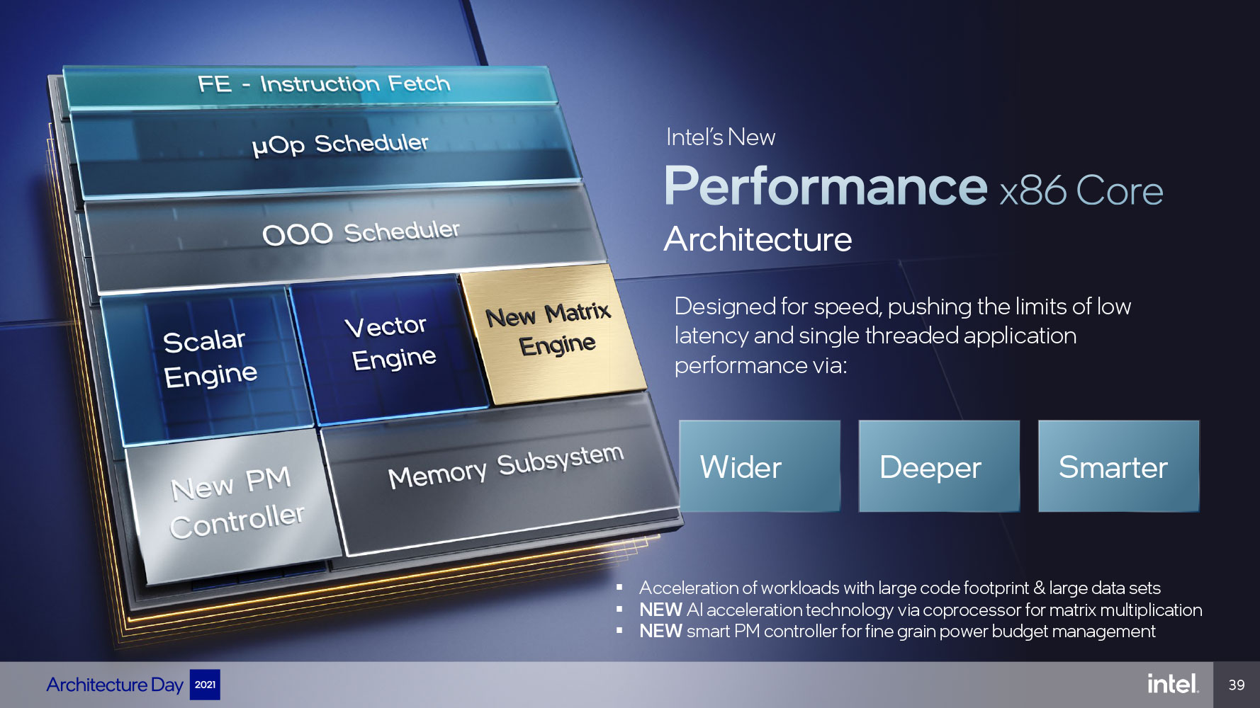
The "Golden Cove" performance core (P-core) features numerical increments to the decode unit, micro-op queue, and micro-op cache. The out-of-order (OoO) engine sees similar increments with 6-wide allocation and 12-wide execution ports, compared to 5-wide allocation and 10-wide execution ports for Cypress Cove. The execution stage sees the addition of a fifth execution port and ALU, FMA with FP16 support, and an updated fast adder (FADD). Similar improvements are made to the cache and memory sub-system. These add toward the 28% IPC uplift for this core.
There are no E-cores physically present on the H0 silicon. With no Hybrid CPU Core architecture present, the Core i5 H0 processor is a traditional multi-core processor that doesn't quite need the Intel Thread Director middleware, although we don't know if Thread Director is absent on these chips or a vestige of it is present.
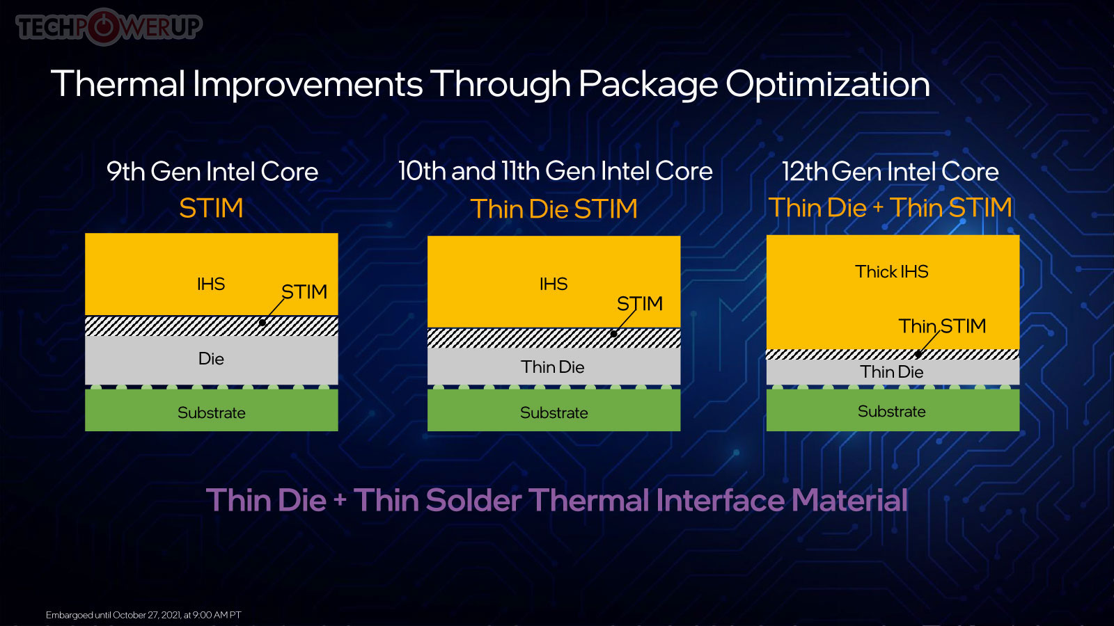
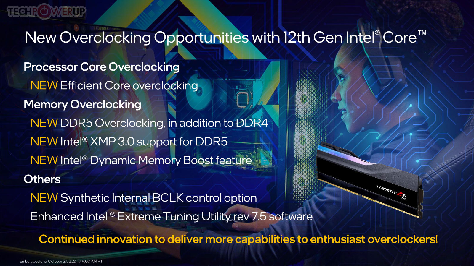
To eke out the best-possible thermals from the 14 nm node it was stuck with, Intel pulled off some innovative ways to transfer heat between the silicon and cooling solution over the past couple of solutions. These innovations continue with Alder Lake. The die and STIM are now thinner, and the copper IHS thicker. Among the new overclocking capabilities are the ability to tweak even the E-cores, DDR5 memory, new XMP 3.0 profiles for DDR5 memory, synthetic BCLK that ensures a base-clock overclock doesn't break sensitive clock domains relying on it, and external clock generation, in addition to the processor's internal clock generator. The Core i5-12600 lacks an unlocked multiplier and hence doesn't offer a multiplier value beyond 48x. You could try playing with the 100 MHz base-clock on a Z690 chipset motherboard as it is de-coupled with other sensitive clock domains, such as PCIe. This, however, requires one of those pricey Z690 boards with discrete clock generators.
Intel Z690 Chipset
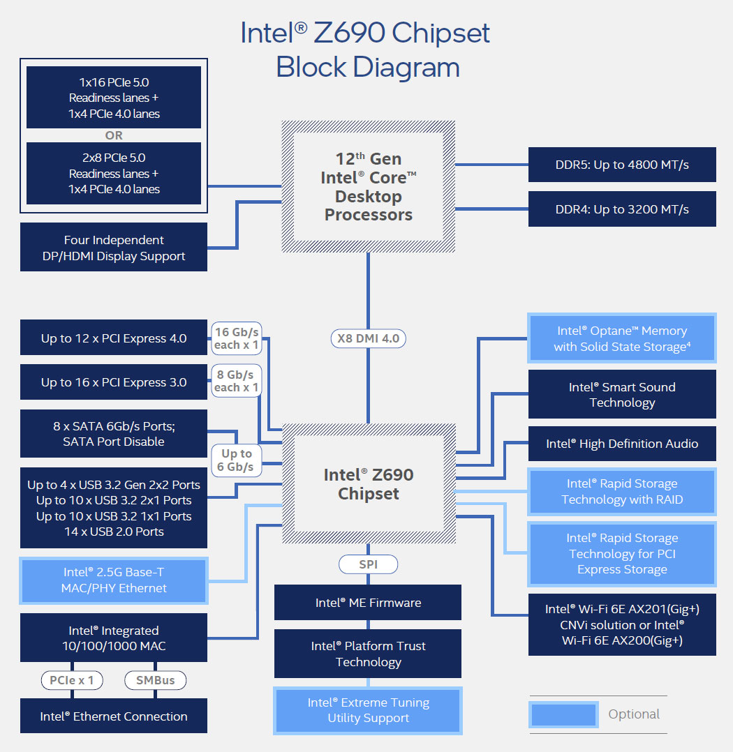
The Z690 chipset is Intel's first client chipset with PCI-Express 4.0 downstream connectivity. It talks to the "Alder Lake-S" processor over the DMI 4.0 x8 chipset bus. Downstream PCIe connectivity includes 12x Gen 4 and 16x Gen 3 PCIe general-purpose lanes. The rest of its chipset-attached connectivity is the same as the Z590, including MIPI SoundWire support, NVMe RAID, 8-port SATA 6 Gbps, and recommended network interfaces that include 2.5 GbE and Wi-Fi 6E.
Intel B660 and H610 Chipsets
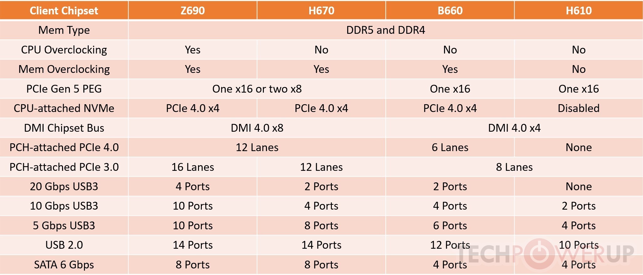
As of this writing, VERY few motherboards use the H670 client chipset, making the B660 Intel's mainstream desktop chipset for those with a "locked" 12th Gen Core processor the best option, those who don't need the I/O options of the Z690 and want to save big on the motherboard. The B660 lacks CPU overclocking support, but permits memory overclocking. Motherboard vendors can choose to give it a PCIe Gen 5 PEG slot, as well as DDR5 memory, although you may come across plenty of motherboards with PCIe Gen4 PEG and DDR4 memory. The B660 chipset uses a narrower 4-lane DMI 4.0 chipset bus than what 12th Gen Core processors are capable of (up to 8 DMI 4.0 lanes). This shouldn't be too much of a problem as the chipset only puts out 6 downstream PCIe Gen4 lanes, besides 8 Gen3 lanes. Motherboard designers should use the downstream Gen4 connectivity to wire out another M.2 Gen4 slot. You also get fewer high-bandwidth USB3 port types. The H610 is the bare entry-level chipset. You lose out on memory overclocking, only get Gen3 PCIe connectivity across the board, and have no CPU-attached NVMe.
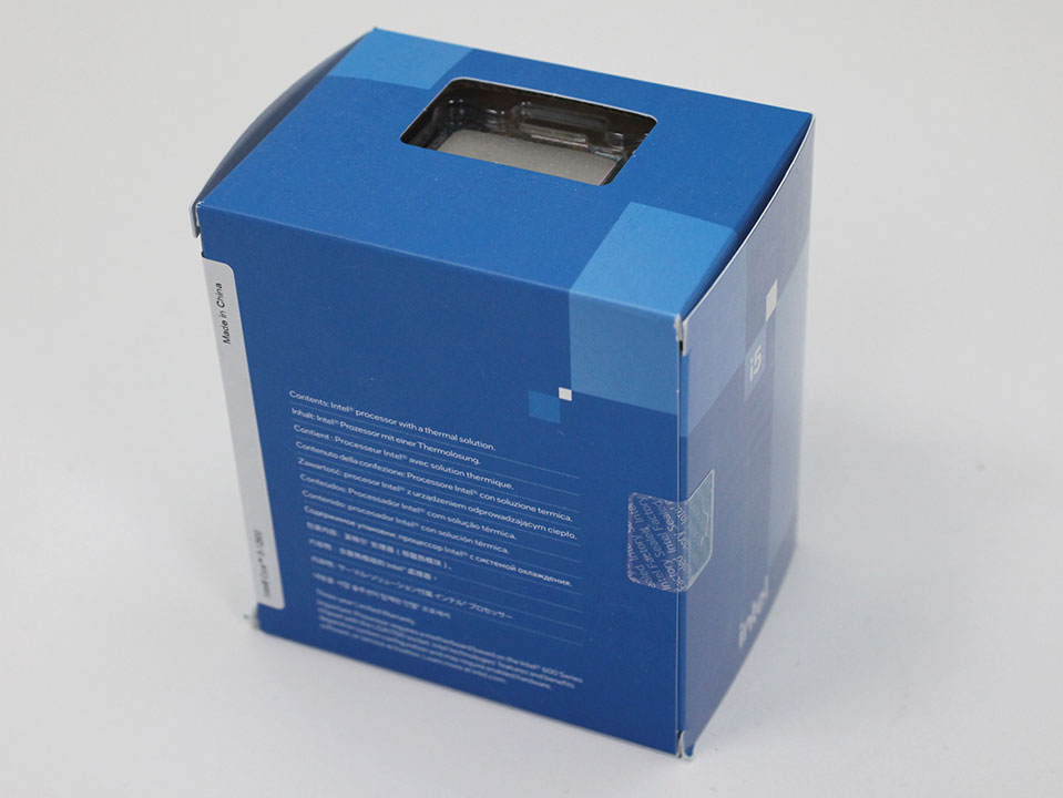
Unboxing and Photography

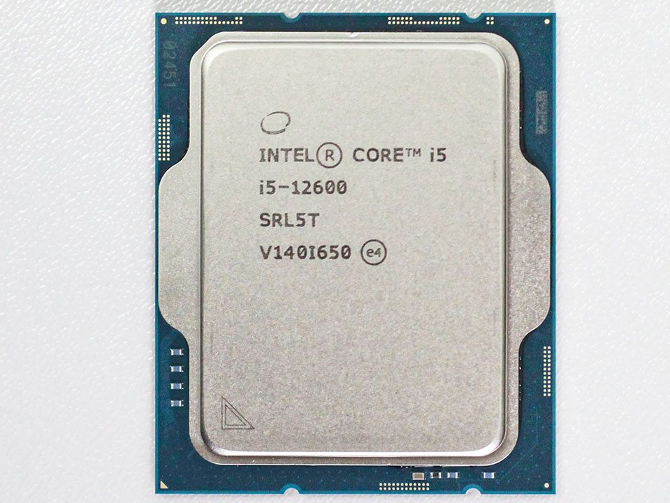
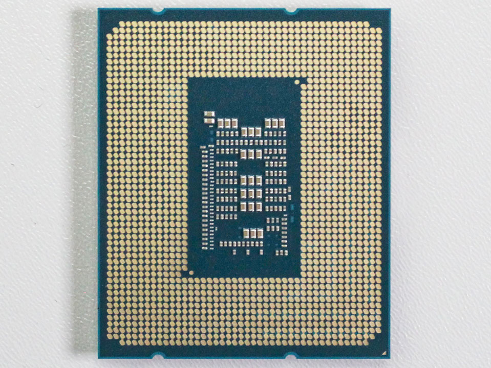
Here it is, the processor itself. It measures 37.5 mm x 45.0 mm and is a more rectangular-looking processor, much like the LGA1366 before it.
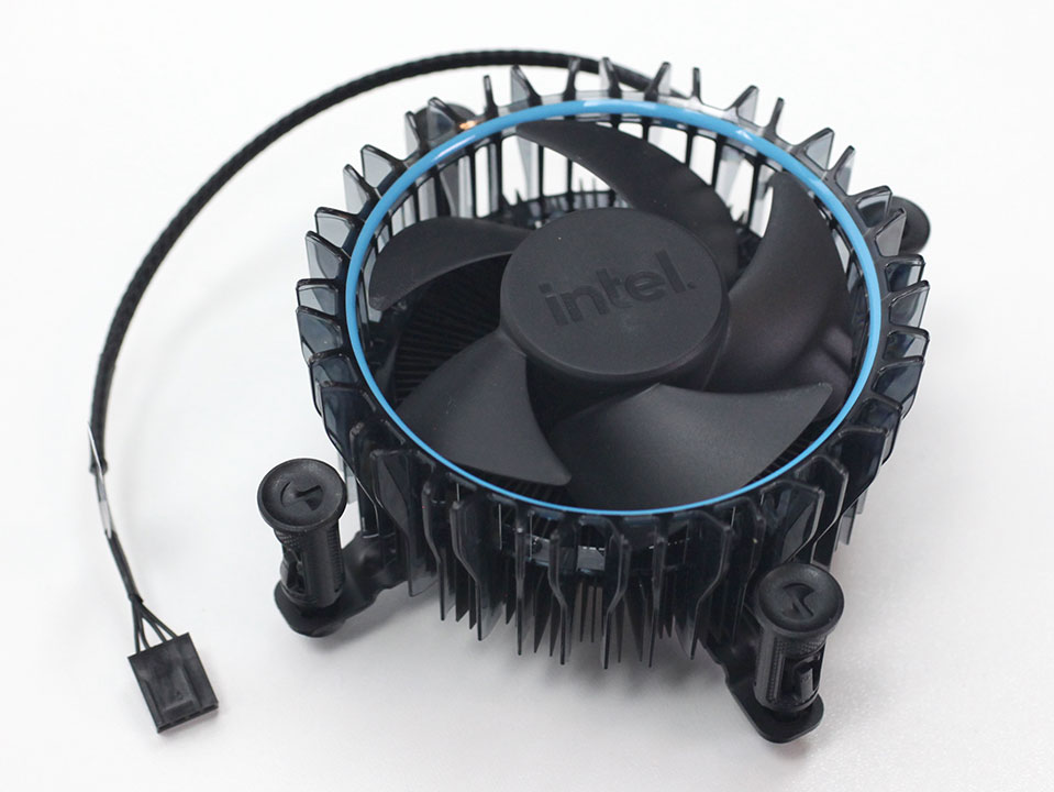
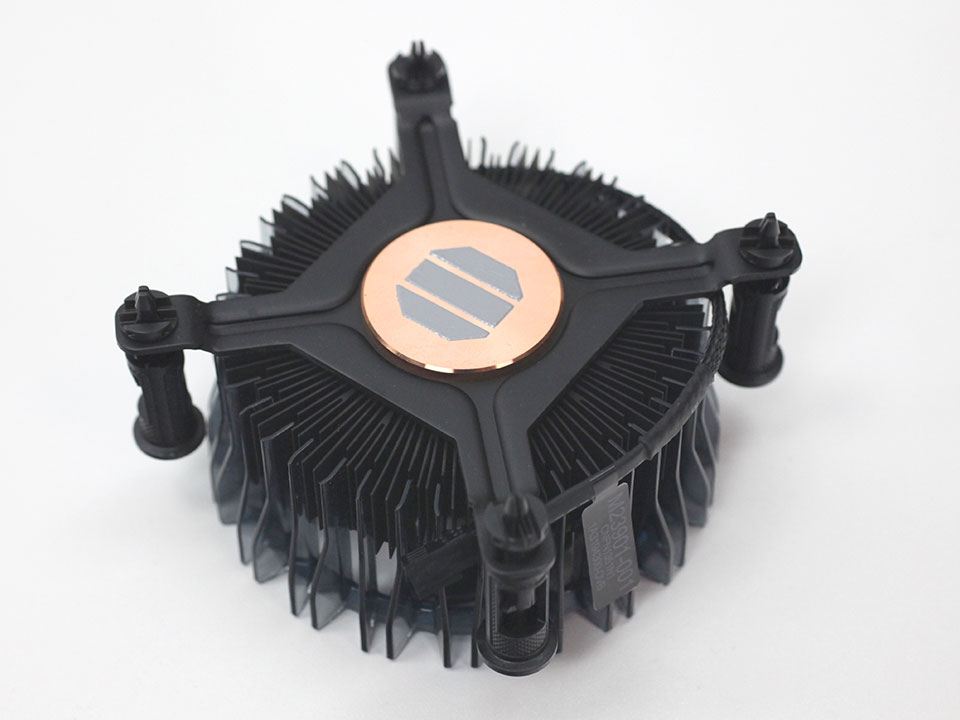
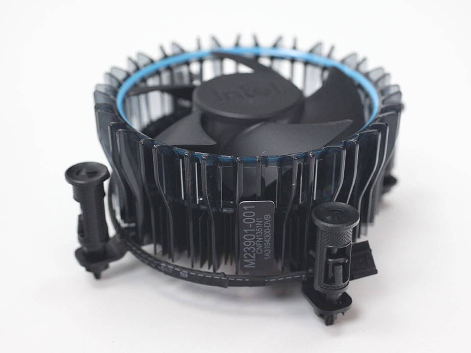
Included in the package is this new Intel stock cooler. It's a relatively simple, compact solution with a copper base.

Intel Socket LGA1700 has an intuitive installation process that should be familiar from many past LGA sockets. Trouble is that it comes with a different cooler mount-hole spacing than LGA1200 and the five different Socket-H series sockets before it, so you'll need to search for a compatible cooler. Most cooler companies are handing out adapters, but those aren't available in all countries.
Test Setup
- All applications, games, and processors are tested with the drivers and hardware listed below—no performance results were recycled between test systems.
- All games and applications are tested using the same version.
- All games are set to their highest quality setting unless indicated otherwise.
| Test System "Alder Lake" | |
|---|---|
| Processor: | All Intel 12th Generation processors |
| Motherboard: | DDR5: ASUS Z690 Maximus Hero / BIOS 0702 DDR4: ASUS Z690 STRIX-A Gaming D4 / BIOS 0705 |
| Memory: | 2x 16 GB G.SKILL Trident Z5 RGB DDR5-6000 36-36-36-76 2T / Gear 2 2x 16 GB G.SKILL Ripjaws V DDR4-3200 16-20-20-34 1T / Gear 1 / DR |
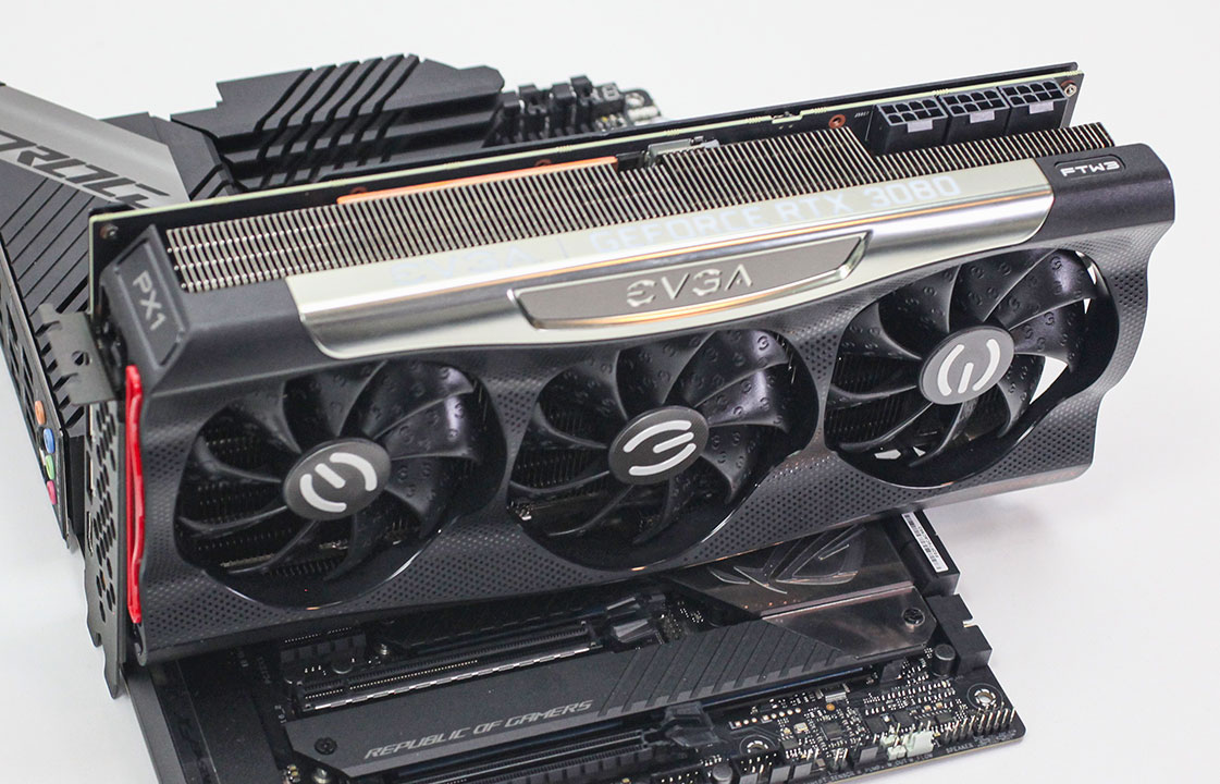
| Graphics: | EVGA GeForce RTX 3080 FTW3 Ultra |
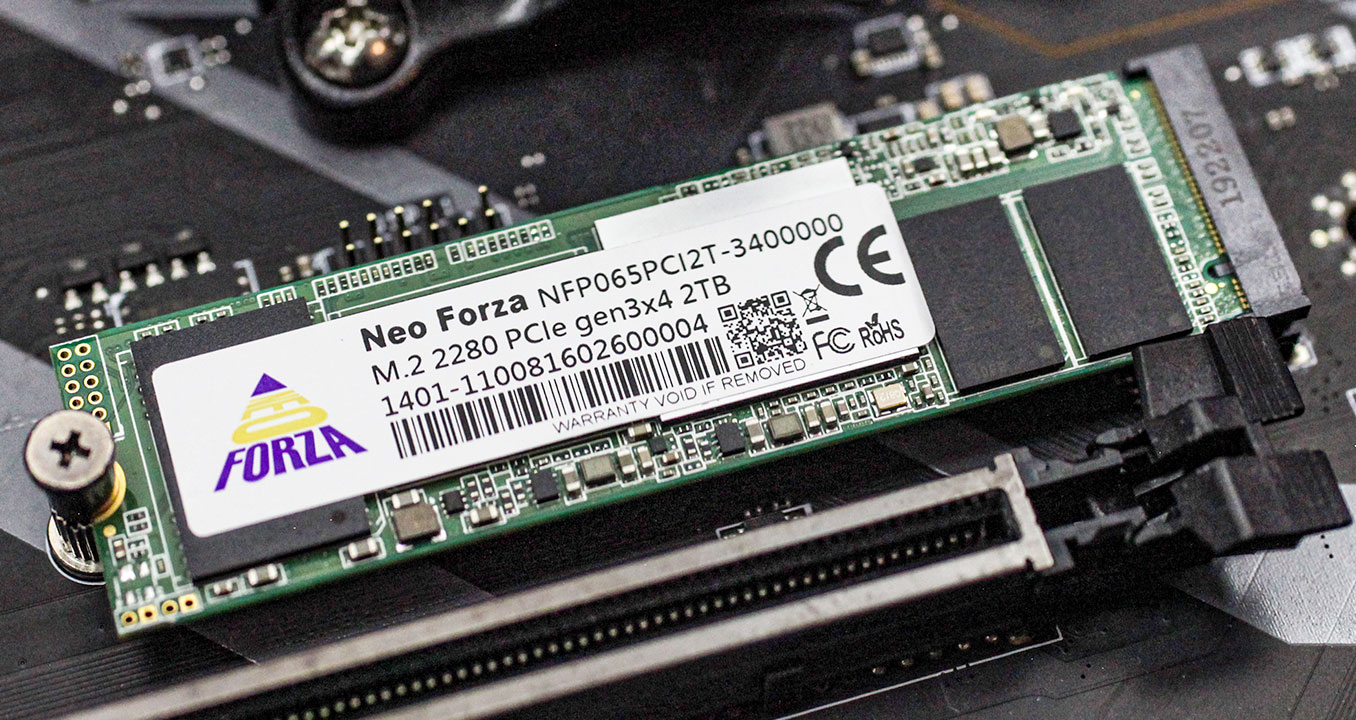
| Storage: | Neo Forza NFP065 1 TB M.2 NVMe SSD |
| Air Cooling: | Noctua NH-U14S |
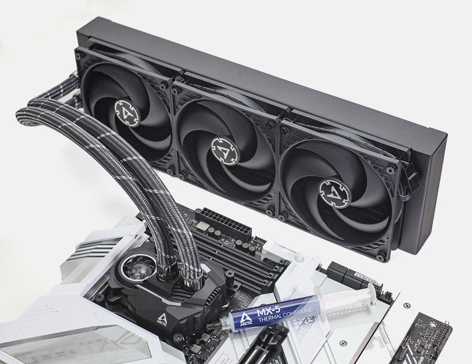
| Water Cooling: | Arctic Liquid Freezer II 360 mm |
| Thermal Paste: | Arctic MX-5 |
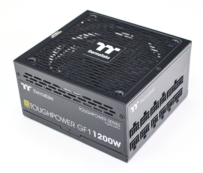
| Power Supply: | Thermaltake Toughpower GF1 1200 W |
| Software: | Windows 11 Professional 64-bit Build 10.0.22000.282 Includes AMD L3 latency fix |
| Drivers: | NVIDIA GeForce 496.49 WHQL |
| Test System "Zen 3" | |
|---|---|
| Processor: | All AMD Ryzen 5000 |
| Motherboard: | MSI MPG X570 Gaming Plus BIOS 7C37vAF3, AGESA 1.2.0.3c |
| Memory: | 2x 16 GB DDR4-3600 16-20-20-34 1T Infinity Fabric @ 1800 MHz 1:1 |
| All other specifications same as above | |
| Test System "Rocket Lake" | |
|---|---|
| Processor: | All Intel 11th Generation processors |
| Motherboard: | ASUS Z590 Maximus XIII Hero BIOS 1007 |
| Memory: | 2x 16 GB DDR4-3600 16-20-20-34 1T Gear 1 |
| All other specifications same as above | |
| Test System "Comet Lake" | |
|---|---|
| Processor: | All Intel 10th Generation processors |
| Motherboard: | ASUS Z490 Maximus XII Extreme BIOS 2301 |
| Memory: | 2x 16 GB DDR4-3600 16-20-20-34 1T |
| All other specifications same as above | |
Super Pi
SuperPi is one of the most popular benchmarks with overclockers and tweakers. It has been used in world-record competitions since forever. It is a purely single-threaded CPU test that calculates Pi to a large number of digits—32 million for our testing. Released in 1995, it only supports x86 floating-point instructions and thus makes for a good test for single-threaded legacy application performance.
Our Patreon Silver Supporters can read articles in single-page format.
Mar 12th, 2025 19:33 EDT
change timezone
Latest GPU Drivers
New Forum Posts
- Packet Loss after updating to windows 11 (7)
- Post your Old CDs & FDs, from back in the day thread. (65)
- RX 9070 availability (218)
- I'm looking for a good tool to make the 3D scanning of my mini-pc using the photogrammetry and my Kinect 2. (71)
- Nvidia's GPU market share hits 90% in Q4 2024 (gets closer to full monopoly) (897)
- PC Audio Speakers Amp/DAC/Receiver/other options? (6)
- The TPU UK Clubhouse (25880)
- X79 and/or rampage IV OC'ing thread for those of us still left.... (2388)
- Bright Memory: Infinite Ray Tracing Benchmark (19)
- CPU downclocks under any loads but it doesn't hit any limits (9)
Popular Reviews
- AMD Ryzen 9 9950X3D Review - Great for Gaming and Productivity
- XFX Radeon RX 9070 XT Mercury OC Magnetic Air Review
- Sapphire Radeon RX 9070 XT Nitro+ Review - Beating NVIDIA
- ASUS Radeon RX 9070 TUF OC Review
- Dough Spectrum Black 32 Review
- FSP MP7 Black Review
- MSI MAG B850 Tomahawk Max Wi-Fi Review
- AMD Ryzen 7 9800X3D Review - The Best Gaming Processor
- NVIDIA GeForce RTX 5070 Founders Edition Review
- Corsair Vengeance RGB CUDIMM DDR5-8800 48 GB CL42 Review
Controversial News Posts
- NVIDIA GeForce RTX 50 Cards Spotted with Missing ROPs, NVIDIA Confirms the Issue, Multiple Vendors Affected (513)
- AMD Radeon RX 9070 and 9070 XT Listed On Amazon - One Buyer Snags a Unit (261)
- AMD RDNA 4 and Radeon RX 9070 Series Unveiled: $549 & $599 (260)
- AMD Mentions Sub-$700 Pricing for Radeon RX 9070 GPU Series, Looks Like NV Minus $50 Again (249)
- NVIDIA Investigates GeForce RTX 50 Series "Blackwell" Black Screen and BSOD Issues (244)
- AMD Radeon RX 9070 and 9070 XT Official Performance Metrics Leaked, +42% 4K Performance Over Radeon RX 7900 GRE (195)
- AMD Radeon RX 9070-series Pricing Leaks Courtesy of MicroCenter (158)
- AMD Radeon RX 9070 XT Could Get a 32 GB GDDR6 Upgrade (100)