 4
4
MSI GeForce RTX 3060 Ti Gaming X Trio Review
Test Setup »High-resolution PCB Pictures
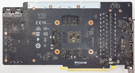
These pictures are for the convenience of volt modders and people who would like to see all the finer details on the PCB. Feel free to link back to us and use these in your articles or forum posts.High-res versions are also available (front, back).
Circuit Board (PCB) Analysis
GPU voltage is 8-phase and managed by an OnSemi NCP81610 controller.
The DrMOS for the GPU are OnSemi 302045 chips.
Memory voltage is a two-phase design generated by a 7222 buck controller.
For memory, Niko Semi PK616BA MOSFETs are used.
The GDDR6 memory chips are made by Samsung and carry the model number K4Z80325BC-HC14. They are specified to run at 1750 MHz (14 Gbps GDDR6 effective).
NVIDIA's GA104 graphics processor is the company's third Ampere architecture chip, the second one targeted at GeForce gamers. It is produced on a 8 nanometer process at Samsung and has a transistor count of 17.4 billion with a die size of 392 mm².
Feb 24th, 2025 02:44 EST
change timezone
Latest GPU Drivers
New Forum Posts
- Why is coil whine still a nuisance? (26)
- Gigabyte AORUS RTX5080 Missing 16 ROP's (32)
- Free Games Thread (4485)
- Keep a 4080s or take a 5070ti? (50)
- What are you playing? (22982)
- Problem with NVIDIA Driver 572.16 and GTX 1080 Ti. (5)
- It's happening again, melting 12v high pwr connectors (906)
- is a 650w gold power supply enough for a amd 7 7700x OR 7 5700x and a msi geforce rtx 4070 super 12go gaming x slim ? (6)
- Your PC ATM (35252)
- What's your latest tech purchase? (23203)
Popular Reviews
- ASUS GeForce RTX 5070 Ti TUF OC Review
- MSI GeForce RTX 5070 Ti Ventus 3X OC Review
- darkFlash DY470 Review
- MSI GeForce RTX 5070 Ti Vanguard SOC Review
- MSI GeForce RTX 5070 Ti Gaming Trio OC+ Review
- Galax GeForce RTX 5070 Ti 1-Click OC White Review
- Palit GeForce RTX 5070 Ti GameRock OC Review
- Fantech Aria II Pro Review
- Gigabyte GeForce RTX 5090 Gaming OC Review
- AMD Ryzen 7 9800X3D Review - The Best Gaming Processor
Controversial News Posts
- NVIDIA GeForce RTX 5090 Spotted with Missing ROPs, NVIDIA Confirms the Issue, Multiple Vendors Affected, RTX 5070 Ti, Too (454)
- AMD Radeon 9070 XT Rumored to Outpace RTX 5070 Ti by Almost 15% (304)
- AMD Plans Aggressive Price Competition with Radeon RX 9000 Series (271)
- AMD Radeon RX 9070 and 9070 XT Listed On Amazon - One Buyer Snags a Unit (247)
- Edward Snowden Lashes Out at NVIDIA Over GeForce RTX 50 Pricing And Value (241)
- AMD Denies Radeon RX 9070 XT $899 USD Starting Price Point Rumors (239)
- NVIDIA Investigates GeForce RTX 50 Series "Blackwell" Black Screen and BSOD Issues (233)
- New Leak Reveals NVIDIA RTX 5080 Is Slower Than RTX 4090 (215)


