 11
11
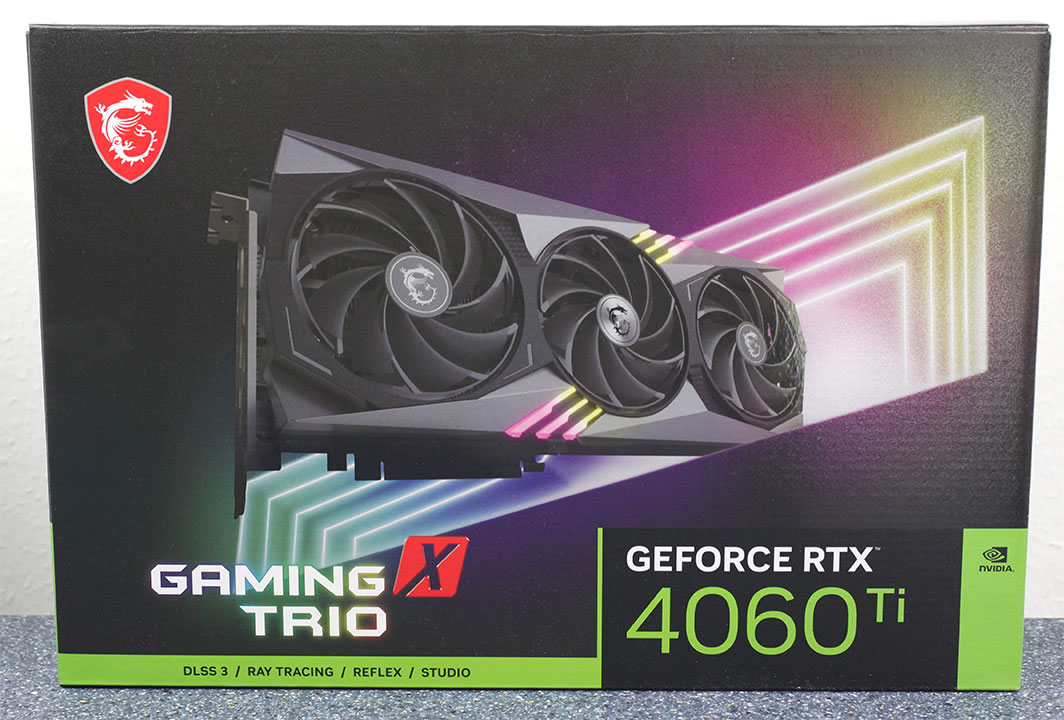
MSI GeForce RTX 4060 Ti Gaming X Trio Review
(11 Comments) »Introduction
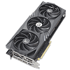
MSI GeForce RTX 4060 Ti Gaming X Trio is the company's most premium custom-design graphics card based on NVIDIA's latest mid-range addition to its RTX 40-series product stack. The card offers, above all, a premium design that looks like it's from a segment above. A well-designed cooler shroud holds a trio of the company's latest-generation TorX fans, which ventilate a TriFrozr 3 cooling solution. The cooler has a neatly-executed RGB LED element. The card also features the company's highest factory-overclock with the RTX 4060 Ti.
The GeForce RTX 4060 Ti Ada is designed to solidify NVIDIA's footing in the hotly contested mid-range, with a starting price of $400 (unchanged from that of the RTX 3060 Ti). It is based on the company's latest Ada Lovelace graphics architecture, which means you get the performance/Watt benefits of the 5 nm foundry node, and exclusive new features such as DLSS 3, a feature by NVIDIA that leverages the Optical Flow Accelerator and Tensor cores, to generate whole frames in gameplay entirely using AI, without involving the graphics rendering machinery. DLSS 3 gains importance in this segment to enable usage of ray tracing, consistent high FPS, or both.
The GeForce RTX 4060 Ti debuts the new 5 nm AD106 silicon to the desktop segment, which it nearly maxes out, featuring 34 out of 36 SM (streaming multiprocessors), which translate to 4,352 CUDA cores, 136 Tensor cores, 34 RT cores, 136 TMUs, and 48 ROPs. While 8 GB of GDDR6 memory is unchanged over the previous generation, NVIDIA has narrowed the memory bus to 128-bit wide. This may seem controversial given its predecessor's 256-bit interface, but NVIDIA has a good explanation for it, which involves large on-die caches, that reduce the dependence on video memory for some of the most frequently accessed data.
The GeForce Ada graphics architecture debuts the latest generation CUDA cores with increased IPC and higher clock speeds, more capable RT cores that accelerate more ray tracing effects on the hardware, and 4th generation Tensor cores with support for newer math formats. The switch to 5 nm means that the typical graphics power of the RTX 4060 Ti is 160 W at reference speeds, which also means premium custom-designs like the MSI RTX 4060 Ti Gaming X Trio can make do with single 8-pin PCIe power connectors, and don't really need the modern 16-pin 12VHPWR connector. MSI is giving the RTX 4060 Ti Gaming X Trio factory-overclocked speeds of 2670 MHz boost, compared to 2535 MHz reference boost. The memory ticks at stock 18 Gbps speeds. MSI is pricing the RTX 4060 Ti Gaming X Trio at $460, a pretty serious premium over the $399 MSRP that brings it close to the $499 MSRP of the upcoming 16 GB variant.
| Price | Cores | ROPs | Core Clock | Boost Clock | Memory Clock | GPU | Transistors | Memory | |
|---|---|---|---|---|---|---|---|---|---|
| RTX 2060 | $180 | 1920 | 48 | 1365 MHz | 1680 MHz | 1750 MHz | TU106 | 10800M | 6 GB, GDDR6, 192-bit |
| RX Vega 64 | $320 | 4096 | 64 | 1247 MHz | 1546 MHz | 953 MHz | Vega 10 | 12500M | 8 GB, HBM2, 2048-bit |
| RX 5700 XT | $180 | 2560 | 64 | 1605 MHz | 1755 MHz | 1750 MHz | Navi 10 | 10300M | 8 GB, GDDR6, 256-bit |
| RTX 3050 | $260 | 2560 | 32 | 1552 MHz | 1777 MHz | 1750 MHz | GA106 | 12000M | 8 GB, GDDR6, 128-bit |
| RTX 2070 | $230 | 2304 | 64 | 1410 MHz | 1620 MHz | 1750 MHz | TU106 | 10800M | 8 GB, GDDR6, 256-bit |
| RX 6600 | $210 | 1792 | 64 | 2044 MHz | 2491 MHz | 1750 MHz | Navi 23 | 11060M | 8 GB, GDDR6, 128-bit |
| RTX 3060 | $300 | 3584 | 48 | 1320 MHz | 1777 MHz | 1875 MHz | GA106 | 12000M | 12 GB, GDDR6, 192-bit |
| RTX 4060 | $300 | 3072 | 32 | 1830 MHz | 2460 MHz | 2125 MHz | AD107 | unknown | 8 GB, GDDR6, 128-bit |
| RX 6600 XT | $250 | 2048 | 64 | 2359 MHz | 2589 MHz | 2000 MHz | Navi 23 | 11060M | 8 GB, GDDR6, 128-bit |
| Arc A750 | $250 | 3584 | 112 | 2050 MHz | N/A | 2000 MHz | ACM-G10 | 21700M | 8 GB, GDDR6, 256-bit |
| Arc A770 | $290 | 4096 | 128 | 2100 MHz | N/A | 2187 MHz | ACM-G10 | 21700M | 16 GB, GDDR6, 256-bit |
| RTX 2080 | $260 | 2944 | 64 | 1515 MHz | 1710 MHz | 1750 MHz | TU104 | 13600M | 8 GB, GDDR6, 256-bit |
| RTX 3060 Ti | $320 | 4864 | 80 | 1410 MHz | 1665 MHz | 1750 MHz | GA104 | 17400M | 8 GB, GDDR6, 256-bit |
| RTX 4060 Ti | $400 | 4352 | 48 | 2310 MHz | 2535 MHz | 2250 MHz | AD106 | 22900M | 8 GB, GDDR6, 128-bit |
| MSI RTX 4060 Ti Gaming X Trio | $460 | 4352 | 48 | 2310 MHz | 2670 MHz | 2250 MHz | AD106 | 22900M | 8 GB, GDDR6, 128-bit |
| RX 6700 XT | $320 | 2560 | 64 | 2424 MHz | 2581 MHz | 2000 MHz | Navi 22 | 17200M | 12 GB, GDDR6, 192-bit |
| RTX 2080 Ti | $400 | 4352 | 88 | 1350 MHz | 1545 MHz | 1750 MHz | TU102 | 18600M | 11 GB, GDDR6, 352-bit |
| RTX 3070 | $350 | 5888 | 96 | 1500 MHz | 1725 MHz | 1750 MHz | GA104 | 17400M | 8 GB, GDDR6, 256-bit |
| RTX 3070 Ti | $420 | 6144 | 96 | 1575 MHz | 1770 MHz | 1188 MHz | GA104 | 17400M | 8 GB, GDDR6X, 256-bit |
Architecture
The Ada graphics architecture heralds the third generation of the NVIDIA RTX technology, an effort toward increasing the realism of game visuals by leveraging real-time ray tracing, without the enormous amount of compute power required to draw purely ray-traced 3D graphics. This is done by blending conventional raster graphics with ray traced elements such as reflections, lighting, and global illumination, to name a few. The 3rd generation of RTX introduces the new higher IPC "Ada" CUDA core, 3rd generation RT core, 4th generation Tensor core, and the new Optical Flow Processor, a component that plays a key role in generating new frames without involving the GPU's main graphics rendering pipeline.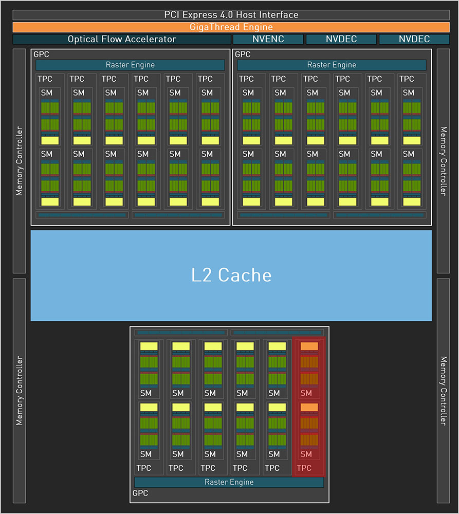


The GeForce Ada graphics architecture driving the RTX 4060 Ti leverages the TSMC 5 nm EUV foundry process to increase transistor counts. At the heart of this GPU is the new AD106 silicon, with a fairly high transistor count of 22.9 billion, which is almost double that of the previous-generation GA106, and still about 30% more than the GA104. The GPU features a generationally narrower PCI-Express 4.0 x8 host interface, and a 128-bit wide GDDR6 memory interface. This is causing some controversy, and we'll present NVIDIA's explanation below. The Optical Flow Accelerator (OFA) is an independent top-level component. The chip features one NVENC and one NVDEC unit.
The essential component hierarchy is similar to past generations of NVIDIA GPUs. The AD106 silicon features 3 Graphics Processing Clusters (GPCs), each of these has all the SIMD and graphics rendering machinery, and is a small GPU in its own right. Each GPC shares a raster engine (geometry processing components) and two ROP partitions (each with eight ROP units). The GPC of the AD106 contains five Texture Processing Clusters (TPCs), the main number-crunching machinery. Each of these has two Streaming Multiprocessors (SM), and a Polymorph unit. Each SM contains 128 CUDA cores across four partitions. Half of these CUDA cores are pure-FP32; while the other half is capable of FP32 or INT32. The SM retains concurrent FP32+INT32 math processing capability. The SM also contains a 3rd generation RT core, four 4th generation Tensor cores, some cache memory, and four TMUs. There are 12 SM per GPC, so 1,536 CUDA cores, 48 Tensor cores, and 12 RT cores; per GPC. There are three such GPCs, which add up to 4,608 CUDA cores, 144 TMUs, 144 Tensor Cores, and 36 RT cores. Each GPC contributes 16 ROPs, so there are 48 ROPs on the silicon. The RTX 4060 Ti is carved out of the AD106 by disabling one TPC worth 256 CUDA cores. This yields 4,352 CUDA cores, 136 Tensor cores, 34 RT cores, and 136 TMUs. The ROP count is untouched at 48, as is the on-die L2 cache sees a slight reduction, which is 32 MB in size.
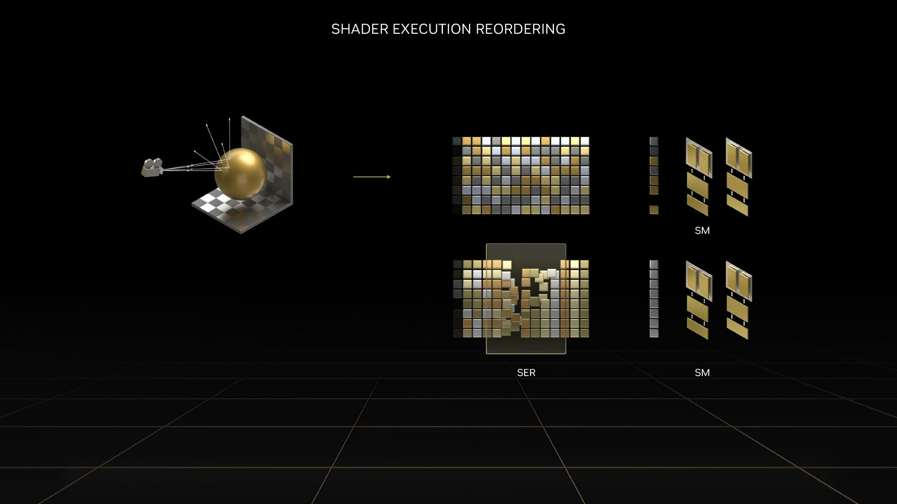

The 3rd generation RT core accelerates the most math-intensive aspects of real-time ray tracing, including BVH traversal. Displaced micro-mesh engine is a revolutionary feature introduced with the new 3rd generation RT core. Just as mesh shaders and tessellation have had a profound impact on improving performance with complex raster geometry, allowing game developers to significantly increase geometric complexity; DMMs is a method to reduce the complexity of the bounding-volume hierarchy (BVH) data-structure, which is used to determine where a ray hits geometry. Previously, the BVH had to capture even the smallest details to properly determine the intersection point. Ada's ray tracing architecture also receives a major performance uplift from Shader Execution Reordering (SER), a software-defined feature that requires awareness from game-engines, to help the GPU reorganize and optimize worker threads associated with ray tracing.
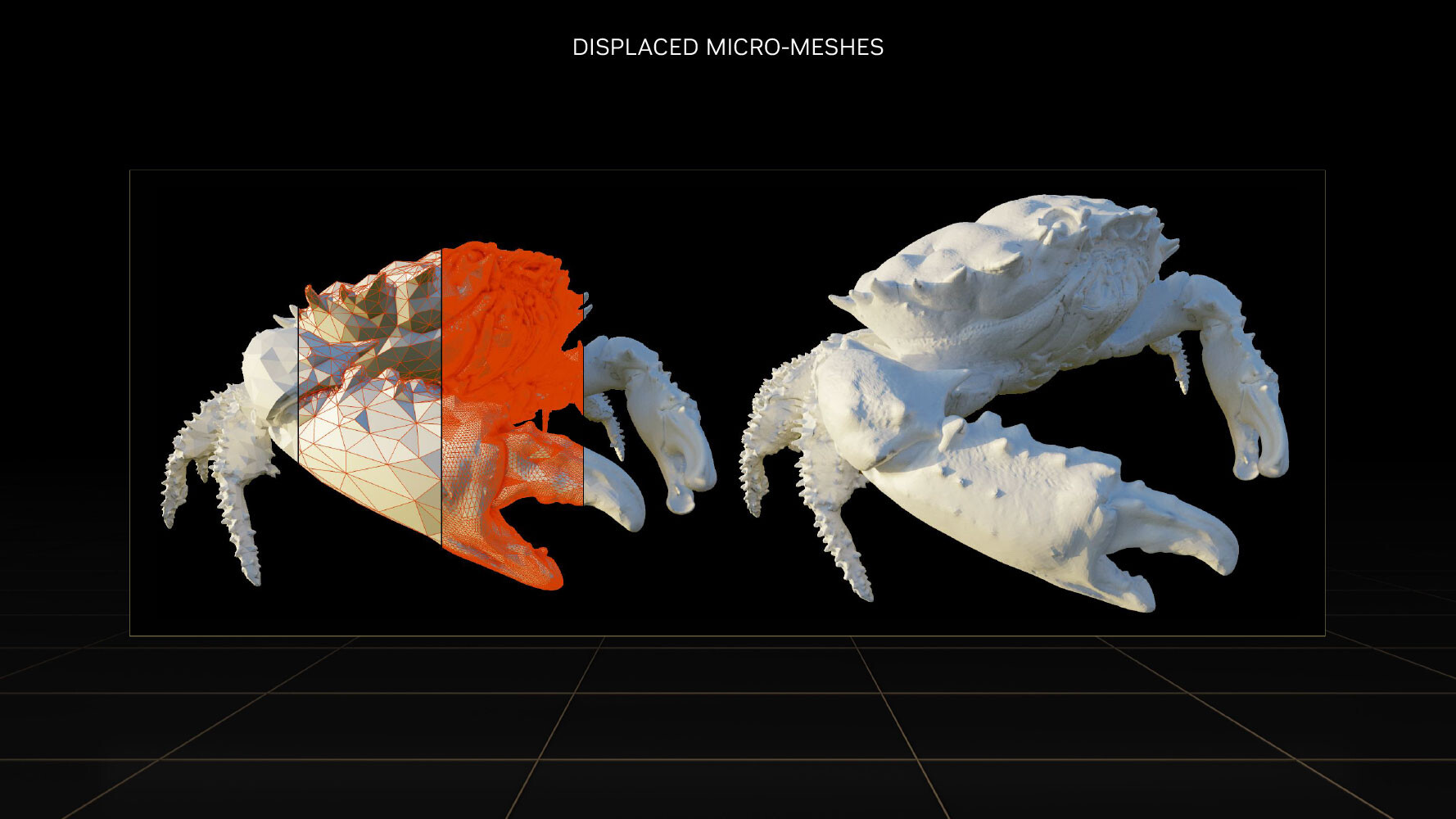
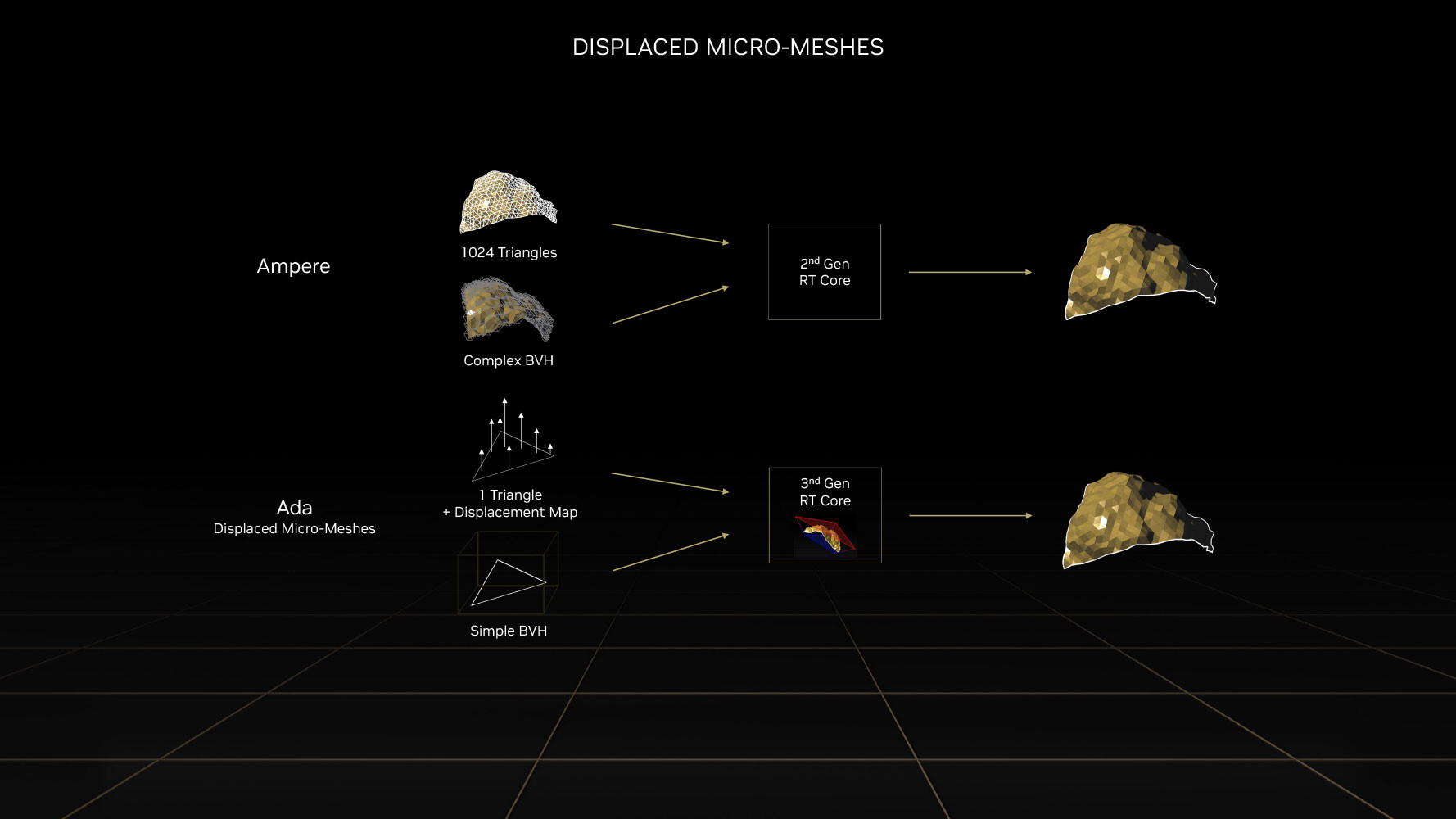
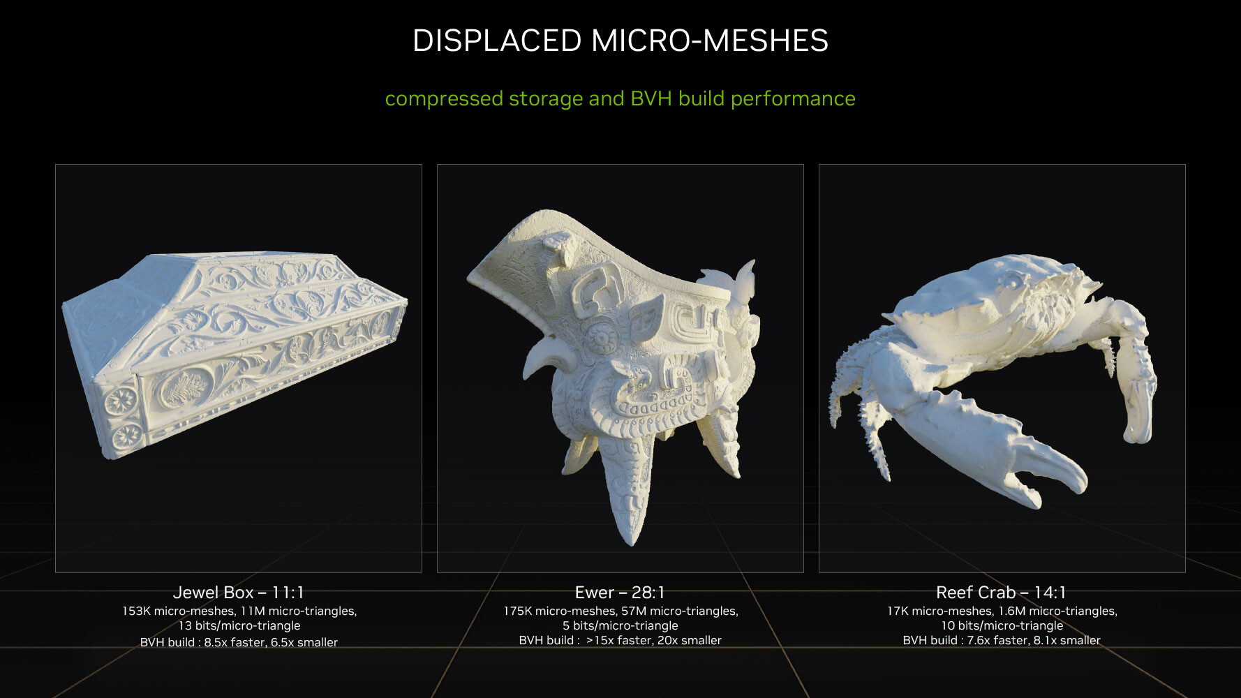
The BVH now needn't have data for every single triangle on an object, but can represent objects with complex geometry as a coarse mesh of base triangles, which greatly simplifies the BVH data structure. A simpler BVH means less memory consumed and helps to greatly reduce ray tracing CPU load, because the CPU only has to generate a smaller structure. With older "Ampere" and "Turing" RT cores, each triangle on an object had to be sampled at high overhead, so the RT core could precisely calculate ray intersection for each triangle. With Ada, the simpler BVH, plus the displacement maps can be sent to the RT core, which is now able to figure out the exact hit point on its own. NVIDIA has seen 11:1 to 28:1 compression in total triangle counts. This reduces BVH compile times by 7.6x to over 15x, in comparison to the older RT core; and reducing its storage footprint by anywhere between 6.5 to 20 times. DMMs could reduce disk- and memory bandwidth utilization, utilization of the PCIe bus, as well as reduce CPU utilization. NVIDIA worked with Simplygon and Adobe to add DMM support for their tool chains.

Opacity Micro Meshes (OMM) is a new feature introduced with Ada to improve rasterization performance, particularly with objects that have alpha (transparency data). Most low-priority objects in a 3D scene, such as leaves on a tree, are essentially rectangles with textures on the leaves where the transparency (alpha) creates the shape of the leaf. RT cores have a hard time intersecting rays with such objects, because they're not really in the shape that they appear (they're really just rectangles with textures that give you the illusion of shape). Previous-generation RT cores had to have multiple interactions with the rendering stage to figure out the shape of a transparent object, because they couldn't test for alpha by themselves.
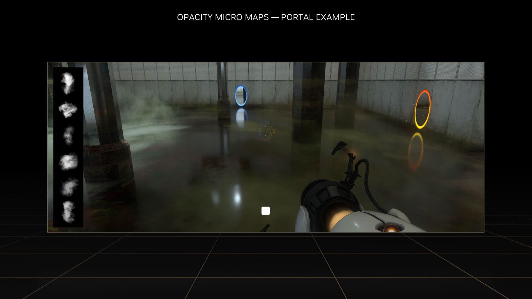

This has been solved by using OMMs. Just as DMMs simplify geometry by creating meshes of micro-triangles; OMMs create meshes of rectangular textures that align with parts of the texture that aren't alpha, so the RT core has a better understanding of the geometry of the object, and can correctly calculate ray intersections. This has a significant performance impact on shading performance in non-RT applications, too. Practical applications of OMMs aren't just low-priority objects such as vegetation, but also smoke-sprites and localized fog. Traditionally there was a lot of overdraw for such effects, because they layered multiple textures on top of each other, that all had to be fully processed by the shaders. Now only the non-opaque pixels get executed—OMMs provide a 30 percent speedup with graphics buffer fill-rates, and a 10 percent impact on frame-rates.


DLSS 3 introduces a revolutionary new feature that promises a doubling in frame-rate at comparable quality, it's called AI frame-generation. While it has all the features of DLSS 2 and its AI super-resolution (scaling up a lower-resolution frame to native resolution with minimal quality loss); DLSS 3 can generate entire frames simply using AI, without involving the graphics rendering pipeline. Later in the article, we will show you DLSS 3 in action.

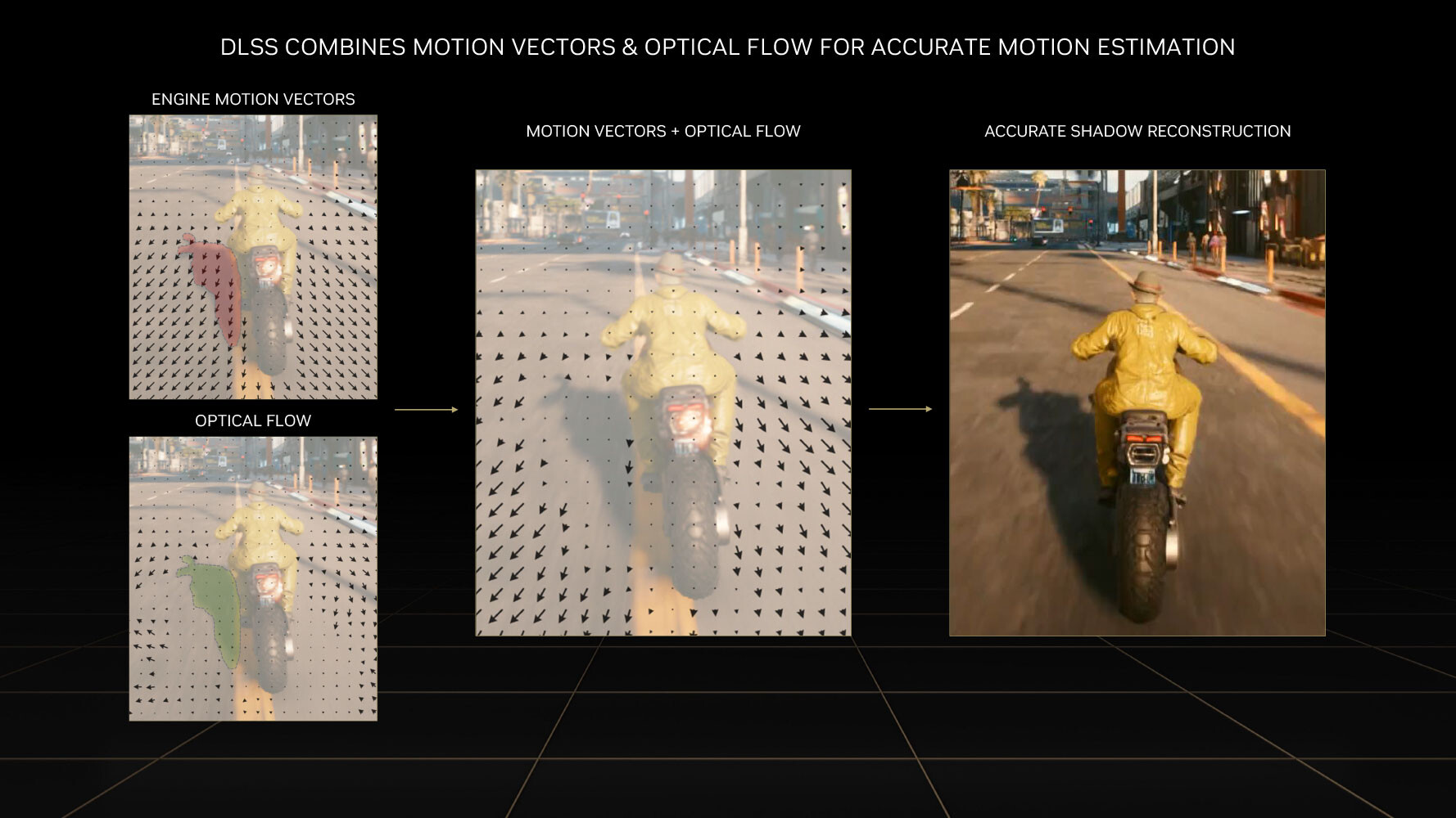
Every alternating frame with DLSS 3 is hence AI-generated, without being a replica of the previous rendered frame. This is possible only on the Ada graphics architecture, because of a hardware component called the optical flow accelerator (OFA), which assists in predicting what the next frame could look like, by creating what NVIDIA calls an optical flow-field. OFA ensures that the DLSS 3 algorithm isn't confused by static objects in a rapidly-changing 3D scene (such as a race sim). The process heavily relies on the performance uplift introduced by the FP8 math format of the 4th generation Tensor core. A third key ingredient of DLSS 3 is Reflex. By reducing the rendering queue to zero, Reflex plays a vital role in ensuring that frame-times with DLSS 3 are at an acceptable level, and a render-queue doesn't confuse the upscaler. A combination of OFA and the 4th Gen Tensor core is why the Ada architecture is required to use DLSS 3, and why it won't work on older architectures.
Ada Rebalanced Memory Subsystem


The previous-generation GeForce RTX 3060 Ti featured a 256-bit wide GDDR6 memory interface driving its 8 GB of 14 Gbps-rated GDDR6 memory (448 GB/s memory bandwidth), which has caused some controversy with the new RTX 4060 Ti using a narrower 128-bit wide memory interface to drive 8 GB of 18 Gbps memory (288 GB/s bandwidth). With the new Ada Lovelace graphics architecture, NVIDIA has tried to re-balance the memory sub-system such that there's dependence on larger on-die caches, allowing NVIDIA to narrow down the GPU's GDDR6 memory interface. The obvious benefit of this to NVIDIA is reduced costs, let's make no mistake about it, but NVIDIA maintains that this isn't a big problem for the GPU.
The last-level cache, or L2 cache, of NVIDIA Ada GPUs is anywhere between 8-10 times larger than the ones on the previous-generation Ampere GPUs. The AD106 silicon powering the RTX 4060 Ti has a 32 MB L2 cache, compared to the 4 MB of the GA104 silicon powering the RTX 3060 Ti. NVIDIA illustrated an example of how a the larger on-die LLC reduces video memory pressure (trips to GDDR6) by anywhere between 40% to 60% on the same GPU, by soaking up a larger number of memory access requests by the shaders.
The L2 cache is unified victim cache to the GPU's various GPCs and their local TPCs. Data that isn't hot enough (frequently accessed enough) to be resident on the small L1 caches of the SM, is ejected to the L2 cache, and depending on its heat, pushed to the GDDR6 video memory. The L2 cache is an order of magnitude faster than than video memory in terms of latency, and so having frequently-accessed data reside there offers a considerable benefit.

As we mentioned earlier from NVIDIA's claims, this re-balancing of the memory sub-system between the on-die LLC and video memory lowers the GPU's access to the latter by as much as 60%, which means the GPU can make do with a narrower 128-bit wide GDDR6 memory bus. NVIDIA has used generationally faster 18 Gbps memory chips in the RTX 4060 Ti. NVIDIA developed a new means of presenting the memory bandwidth that takes into account the contribution of the L2 cache, its hit-rate, and the consequent reduction in video memory traffic. While the memory bandwidth of the RTX 4060 Ti is 288 GB/s, NVIDIA claims that its "effective bandwidth" is 554 GB/s (23% higher than the 448 GB/s memory bandwidth of the RTX 3060 Ti). It's interesting to point out that NVIDIA has used "effective bandwidth" figures in the past to highlight its lossless memory compression technologies, but has never been this vocal about it.
Packaging
The Card
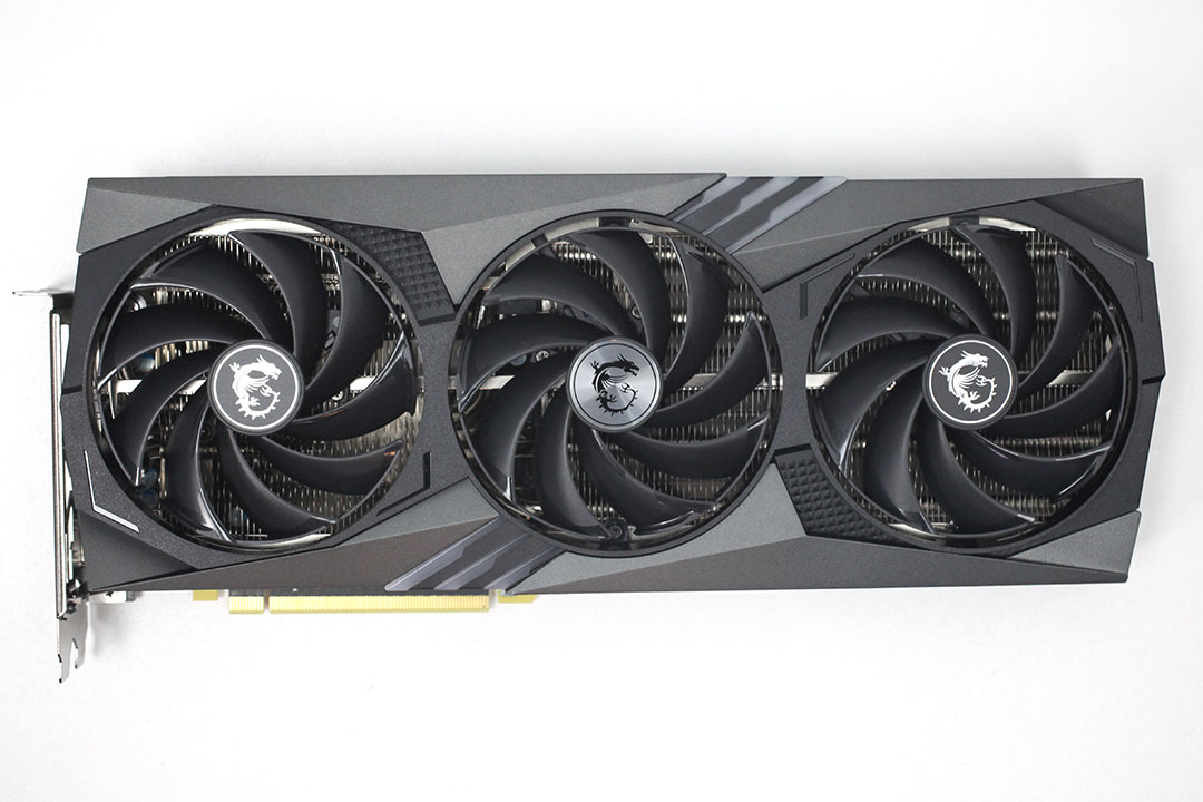


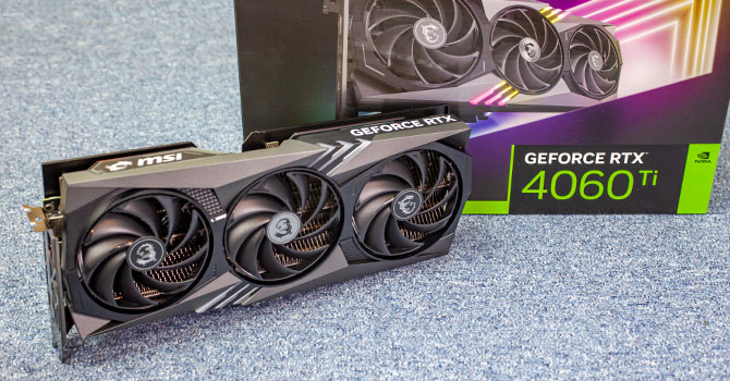
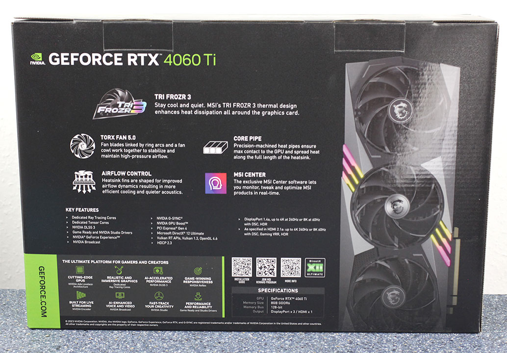
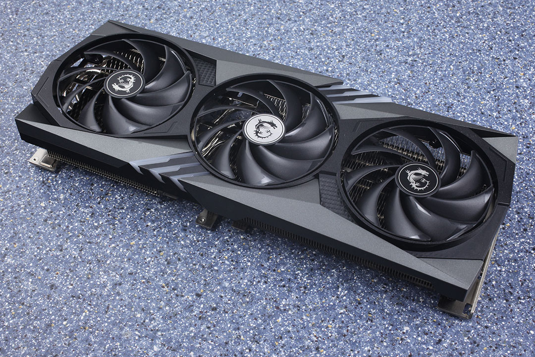
MSI RTX 4060 Ti Gaming X Trio uses a very premium-looking cooling solution the company calls TriFrozr 3. The cooler shroud, made of metal and plastic bits, has plenty going on by the way of design cuts and creases. The backplate has a large opening, so nearly half of the card's airflow is vented right through the heatsink.

The card's main RGB lighting is neatly executed around the middle fan. The MSI logo in the top left is lit up, too.
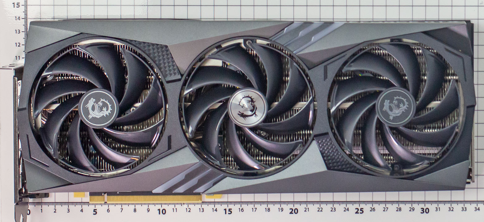
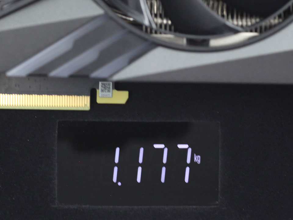
Dimensions of the card are 33.0 x 14.0 cm, and it weighs 1.17 kg.

Installation requires three slots in your system.

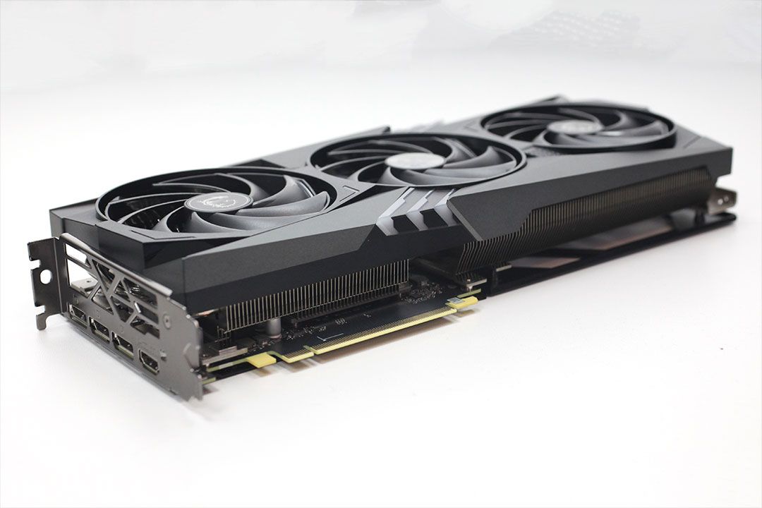
Display connectivity includes three standard DisplayPort 1.4a ports and one HDMI 2.1a (same as Ampere).
The new 8th Gen NVENC now accelerates AV1 encoding, besides HEVC. You also get an "optical flow accelerator" unit that is able to calculate intermediate frames for videos, to smooth playback. The same hardware unit is used for frame generation in DLSS 3.

MSI opted for a single 8-pin PCIe power connector.
Teardown
The cooler is held together by a set of screws that hold the backplate, PCB, and cooler together.

This is easily the most elaborate cooling solution for an RTX 4060 Ti we've seen so far. A nickel-plated copper base-plate pulls heat from the GPU and memory, additional sets of such base-plates do so from the VRM. There are two large aluminium fin-stacks arranged on either ends of the heatpipes.

MSI uses five nickel-plated copper heatpipes.


A high quality metal backplate is used. This has a large opening that allows airflow from nearly half of the cooler to go right through.
High-resolution PCB Pictures
These pictures are for the convenience of volt modders and people who would like to see all the finer details on the PCB. Feel free to link back to us and use these in your articles, videos or forum posts.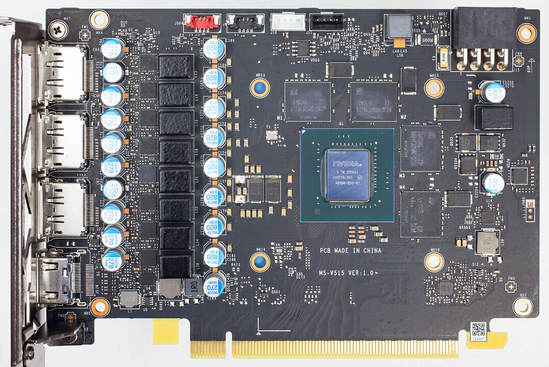
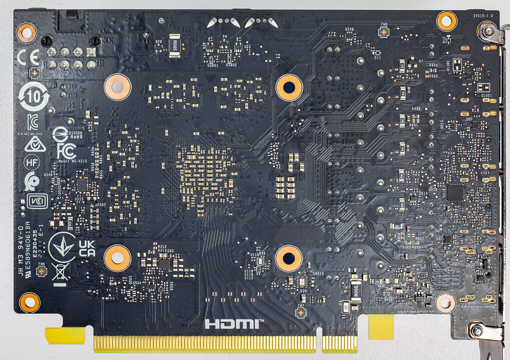
High-resolution versions are also available (front, back).
Our Patreon Silver Supporters can read articles in single-page format.
Mar 12th, 2025 19:34 EDT
change timezone
Latest GPU Drivers
New Forum Posts
- Packet Loss after updating to windows 11 (7)
- Post your Old CDs & FDs, from back in the day thread. (65)
- RX 9070 availability (218)
- I'm looking for a good tool to make the 3D scanning of my mini-pc using the photogrammetry and my Kinect 2. (71)
- Nvidia's GPU market share hits 90% in Q4 2024 (gets closer to full monopoly) (897)
- PC Audio Speakers Amp/DAC/Receiver/other options? (6)
- The TPU UK Clubhouse (25880)
- X79 and/or rampage IV OC'ing thread for those of us still left.... (2388)
- Bright Memory: Infinite Ray Tracing Benchmark (19)
- CPU downclocks under any loads but it doesn't hit any limits (9)
Popular Reviews
- AMD Ryzen 9 9950X3D Review - Great for Gaming and Productivity
- XFX Radeon RX 9070 XT Mercury OC Magnetic Air Review
- Sapphire Radeon RX 9070 XT Nitro+ Review - Beating NVIDIA
- ASUS Radeon RX 9070 TUF OC Review
- Dough Spectrum Black 32 Review
- FSP MP7 Black Review
- MSI MAG B850 Tomahawk Max Wi-Fi Review
- AMD Ryzen 7 9800X3D Review - The Best Gaming Processor
- NVIDIA GeForce RTX 5070 Founders Edition Review
- Corsair Vengeance RGB CUDIMM DDR5-8800 48 GB CL42 Review
Controversial News Posts
- NVIDIA GeForce RTX 50 Cards Spotted with Missing ROPs, NVIDIA Confirms the Issue, Multiple Vendors Affected (513)
- AMD Radeon RX 9070 and 9070 XT Listed On Amazon - One Buyer Snags a Unit (261)
- AMD RDNA 4 and Radeon RX 9070 Series Unveiled: $549 & $599 (260)
- AMD Mentions Sub-$700 Pricing for Radeon RX 9070 GPU Series, Looks Like NV Minus $50 Again (249)
- NVIDIA Investigates GeForce RTX 50 Series "Blackwell" Black Screen and BSOD Issues (244)
- AMD Radeon RX 9070 and 9070 XT Official Performance Metrics Leaked, +42% 4K Performance Over Radeon RX 7900 GRE (195)
- AMD Radeon RX 9070-series Pricing Leaks Courtesy of MicroCenter (158)
- AMD Radeon RX 9070 XT Could Get a 32 GB GDDR6 Upgrade (100)