 49
49
NVIDIA GeForce GTX 750 Ti 2 GB Review
Packaging & Contents »Architecture
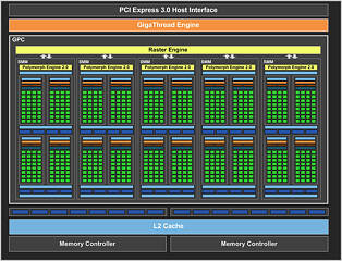
NVIDIA's primary design goal with the GM107 is to up the performance-per-watt game. If NVIDIA achieves a significant performance-per-watt gain with "Maxwell" over "Kepler," it can trade that gain for performance on bigger "Maxwell" chips bolstered by the 20 nm process. It's this fact that makes the GK107 academically interesting.As we mentioned earlier, the GM107 essentially features the same component hierarchy as previous generation "Kepler" GPUs, but introduces changes to the design of the streaming multiprocessor (SMM), the parallel-processing sub-unit of the GPU. At its outermost ring, the GM107 features the GigaThread Engine, a component that marshals data and instructions between the graphics processing cluster (GPC), the raster operations processors (ROPs), the L3 cache, the memory controllers, the bus interface, and the display I/O.
Several GPCs can typically be routed to a GigaThread engine, but being a mid-range GPU, the GM107 features just one. This GPC features a raster engine that handles high-level assembly of data and instructions and five streaming multiprocessors (SMMs), which is where the number crunching takes place. Unlike the streaming multiprocessors (SMXs) of "Kepler" GPUs, which feature an incoherent group of 192 CUDA cores, the SMM features four groups of 32 cores each, which totals 128 per SMM. The SMM shares a Polymorph Engine that features components such as the tessellator, fetch, setup, transform, and stream output with the four groups. The four groups of 32 CUDA cores, each, feature dedicated warp schedulers and registers, with a texture cache cushioning transfers between the groups and TMUs. The GM107 hence features a total of 640 CUDA cores and 48 TMUs. At a higher level, the chip features 16 color ROPs and a 128-bit wide GDDR5 memory interface.
Mar 28th, 2025 01:19 EDT
change timezone
Latest GPU Drivers
New Forum Posts
- TPU's Nostalgic Hardware Club (20133)
- 8 cores cpu (11)
- Is RX 9070 VRAM temperature regular value or hotspot? (243)
- Smelly brand new graphic cards? Remanufactured? (10)
- Core 200s (Bartlett Lake-S) Announced at CES 2025 (26)
- How's your old spinner holding up? (66)
- How is my CPU's temperature? (18)
- Have you got pie today? (16649)
- The TPU UK Clubhouse (25982)
- Post your CrystalDiskMark speeds (615)
Popular Reviews
- Sapphire Radeon RX 9070 XT Pulse Review
- Samsung 9100 Pro 2 TB Review - The Best Gen 5 SSD
- Assassin's Creed Shadows Performance Benchmark Review - 30 GPUs Compared
- Pulsar Feinmann F01 Review
- ASRock Phantom Gaming B860I Lightning Wi-Fi Review
- be quiet! Pure Rock Pro 3 Black Review
- Sapphire Radeon RX 9070 XT Nitro+ Review - Beating NVIDIA
- ASRock Radeon RX 9070 XT Taichi OC Review - Excellent Cooling
- ASUS ProArt X870E-Creator Wi-Fi Review
- AMD Ryzen 7 9800X3D Review - The Best Gaming Processor
Controversial News Posts
- AMD RDNA 4 and Radeon RX 9070 Series Unveiled: $549 & $599 (260)
- MSI Doesn't Plan Radeon RX 9000 Series GPUs, Skips AMD RDNA 4 Generation Entirely (142)
- Microsoft Introduces Copilot for Gaming (123)
- AMD Radeon RX 9070 XT Reportedly Outperforms RTX 5080 Through Undervolting (118)
- NVIDIA Reportedly Prepares GeForce RTX 5060 and RTX 5060 Ti Unveil Tomorrow (115)
- Over 200,000 Sold Radeon RX 9070 and RX 9070 XT GPUs? AMD Says No Number was Given (100)
- NVIDIA GeForce RTX 5050, RTX 5060, and RTX 5060 Ti Specifications Leak (96)
- Retailers Anticipate Increased Radeon RX 9070 Series Prices, After Initial Shipments of "MSRP" Models (90)

