 96
96
NVIDIA GeForce GTX 780 3 GB Review
(96 Comments) »Introduction
The past five years of GPU product launches have shown that fourteen months can be a pretty long time to hold on to a product stack. After an unexpected launch of its 'wildcard' this February, the GeForce GTX Titan, NVIDIA turned its attention to its new-generation GeForce GTX 700 series piloted by the GeForce GTX 780 we have with us today. NVIDIA's choice of naming for the GTX Titan puts it in neither the GTX 600 nor the GTX 700 series. It's just three months old, is holding on to a single-GPU performance lead unassailable by AMD, and has a $1000 price-tag. Its introduction didn't affect prices of GeForce GTX 680 cards, or anything below it, so NVIDIA clearly gunned for the premium. People bought into it, and owners we spoke to are extremely happy with it. We wonder how today's launch will affect them.

The GeForce GTX 780 has a lot in common with the GTX Titan. The two cards are virtually indistinguishable unless you notice the lack of memory chips on the backside of the GTX 780. The two cards are based on the same 28 nm GK110 silicon, almost the same PCB, and most certainly the same space-age cooling solution that helped people draw their heavy wallets out for a $1000 invoice.
There are two ways you can look at the GeForce GTX 780 on paper. Next to its rightful predecessor, the GeForce GTX 680, it offers 50 percent more CUDA cores, 50 percent more memory and memory bandwidth; but next to the GeForce GTX TITAN, it offers fewer cores and half the memory amount. Since the GTX 680 and GTX 780 are based on the same "Kepler" micro-architecture, making an apples-to-apples comparison of their specifications possible, the GeForce GTX 780 is a much better equipped successor than the GeForce GTX 580 was to the GeForce GTX 480 (both of which were based on the "Fermi" micro-architecture).

NVIDIA carved the GeForce GTX 780 out of the GK110 by enabling 12 out of 15 streaming multi-processors on die, which works out to 2,304 CUDA cores. This sets the texture memory unit count to 192, a 50 percent increase over its predecessor's 128. The memory bus is left untouched at 384-bit width, the GPU still packs five graphics processing clusters, and 48 ROPs (yet another 50 percent increase). The reference design card we're putting under the knife in this review features 3 GB of GDDR5 memory. 6 GB non-reference designs by NVIDIA's partners are possible in the future. The GeForce GTX 780 features GPU Boost 2.0, a dynamic overclocking technology that was introduced by the GTX Titan. The technology increases GPU clock speeds, and the voltages required to support them, while factoring in temperatures.

The most interesting part of the GeForce GTX 780 is its positioning in the product stack. It is priced at $649.99, which is much higher than the $499.99 the GeForce GTX 680 asked for when it went on to dethrone the $549.99 Radeon HD 7970 but significantly less than the $999.99 the GTX Titan commands. A card that looks virtually indistinguishable to the GTX Titan when installed is now being offered at two-thirds its price.
| GeForce GTX 670 | Radeon HD 7970 | HD 7970 GHz Ed. | GeForce GTX 680 | GeForce GTX 780 | GeForce GTX 590 | GeForce GTX Titan | GeForce GTX 690 | HD 7990 | |
|---|---|---|---|---|---|---|---|---|---|
| Shader Units | 1344 | 2048 | 2048 | 1536 | 2304 | 2x 512 | 2688 | 2x 1536 | 2x 2048 |
| ROPs | 32 | 32 | 32 | 32 | 48 | 2x 48 | 48 | 2x 32 | 2x 32 |
| Graphics Processor | GK104 | Tahiti | Tahiti | GK104 | GK110 | 2x GF110 | GK110 | 2x GK104 | 2x Tahiti |
| Transistors | 3500M | 4310M | 4310M | 3500M | 7100M | 2x 3000M | 7100M | 2x 3500M | 2x 4310M |
| Memory Size | 2048 MB | 3072 MB | 3072 MB | 2048 MB | 3072 MB | 2x 1536 MB | 6144 MB | 2x 2048 MB | 2x 3072 MB |
| Memory Bus Width | 256 bit | 384 bit | 384 bit | 256 bit | 384 bit | 2x 384 bit | 384 bit | 2x 256 bit | 2x 384 bit |
| Core Clock | 915 MHz+ | 925 MHz | 1050 MHz | 1006 MHz+ | 863 MHz+ | 607 MHz | 837 MHz+ | 915 MHz+ | 1000 MHz |
| Memory Clock | 1502 MHz | 1375 MHz | 1500 MHz | 1502 MHz | 1502 MHz | 855 MHz | 1502 MHz | 1502 MHz | 1500 MHz |
| Price | $370 | $380 | $450 | $430 | $650 | $750 | $1020 | $1000 | $1050 |
Packaging

We received our card in a black, shiny NVIDIA package that seems to act as a placeholder for the final packaging design. I have to admit that this looks much better than a card wrapped in bubble wrap.
Final retail cards will include the usual goodies, like power cables, DVI adapter, and game coupons.
The Card


Visually, the GTX 780 looks exactly like the GTX Titan, except for the GTX 780 markings on the left side of the cooler. The metal unibody looks and feels awesome and puts the product on a completely different level. The card is 26.5 cm long and 11 cm high.

Installing the card requires two slots in your system.
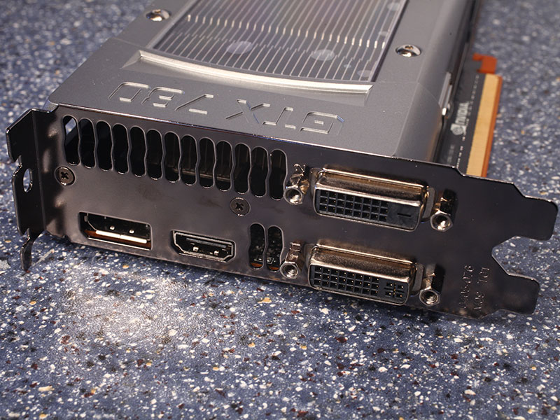
Display connectivity options include two DVI ports, one HDMI port, and one DisplayPort. You may use all outputs at the same time, so triple-monitor surround gaming is possible with one card.
The GPU also includes an HDMI sound device. It is HDMI 1.4a compatible, which includes HD audio and Blu-ray 3D movies support.

Two SLI connectors are available, which would allow you to combine up to four GTX 780 cards in a Triple-SLI, multi-GPU configuration. NVIDIA limited the GTX 780 to Triple-SLI only, while Quad SLI is supported by the GTX Titan.


Pictured above are the front and back, showing the disassembled board. High-res versions are also available (front, back). If you choose to use these images for voltmods, etc., please include a link back to this site, or let us post your article.
A Closer Look


NVIDIA's cooler uses a complex heatsink-base that uses a vapor-chamber technology to cool the GPU, memory chips, and all secondary components. A backplate has not been included.

The card requires one 6-pin and one 8-pin PCI-Express power cable for operation. This power configuration is good for up to 300 W of power draw.

NVIDIA uses the same OnSemi NCP4206 voltage controller on the GTX 780 as on the Titan. It is a cost-effective solution that does not provide any I2C, so advanced monitoring is not possible. Please note how it sits on its own PCB, so we could see different voltage controllers in the future. The GTX 680 uses a similar approach, but the variety of voltage controllers was relatively low.

The GDDR5 memory chips are made by Samsung and carry the model number K4G20325FD-FC03. They are specified to run at 1500 MHz (6000 MHz GDDR5 effective).

NVIDIA's GK110 graphics processor was first introduced as a Tesla-only product for powering demanding GPU compute applications. NVIDIA has now also released it as a GeForce GPU. It uses 7.1 billion transistors on a die size that we measured to be 561 mm². The GPU is produced on a 28 nanometer process at TSMC, Taiwan.
Our Patreon Silver Supporters can read articles in single-page format.
Mar 27th, 2025 19:43 EDT
change timezone
Latest GPU Drivers
New Forum Posts
- Folding Pie and Milestones!! (9448)
- 9070 XT - 2x HDMI high refresh displays (144 and 120 Hz) not working (66)
- Post your cooling. (193)
- Biostar RX 6700 XT OC BIOS (18)
- Future-proofing my OLED (27)
- TPU's Nostalgic Hardware Club (20131)
- The future of RDNA on Desktop. (164)
- How is my CPU's temperature? (17)
- Post your Monster Hunter Wilds benchmark scores (150)
- The TPU UK Clubhouse (25980)
Popular Reviews
- be quiet! Pure Rock Pro 3 Black Review
- Assassin's Creed Shadows Performance Benchmark Review - 30 GPUs Compared
- Sapphire Radeon RX 9070 XT Pulse Review
- Samsung 9100 Pro 2 TB Review - The Best Gen 5 SSD
- Pulsar Feinmann F01 Review
- ASRock Phantom Gaming B860I Lightning Wi-Fi Review
- ASRock Radeon RX 9070 XT Taichi OC Review - Excellent Cooling
- Sapphire Radeon RX 9070 XT Nitro+ Review - Beating NVIDIA
- ASUS ProArt X870E-Creator Wi-Fi Review
- ASUS GeForce RTX 5070 TUF OC Review
Controversial News Posts
- AMD RDNA 4 and Radeon RX 9070 Series Unveiled: $549 & $599 (260)
- MSI Doesn't Plan Radeon RX 9000 Series GPUs, Skips AMD RDNA 4 Generation Entirely (142)
- Microsoft Introduces Copilot for Gaming (123)
- AMD Radeon RX 9070 XT Reportedly Outperforms RTX 5080 Through Undervolting (118)
- NVIDIA Reportedly Prepares GeForce RTX 5060 and RTX 5060 Ti Unveil Tomorrow (115)
- Over 200,000 Sold Radeon RX 9070 and RX 9070 XT GPUs? AMD Says No Number was Given (100)
- NVIDIA GeForce RTX 5050, RTX 5060, and RTX 5060 Ti Specifications Leak (96)
- Retailers Anticipate Increased Radeon RX 9070 Series Prices, After Initial Shipments of "MSRP" Models (90)