 286
286
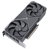
NVIDIA GeForce RTX 5070 Founders Edition Review
Test Setup »High-resolution PCB Pictures
These pictures are for the convenience of volt modders and people who would like to see all the finer details on the PCB. Feel free to link back to us and use these in your articles, videos or forum posts.
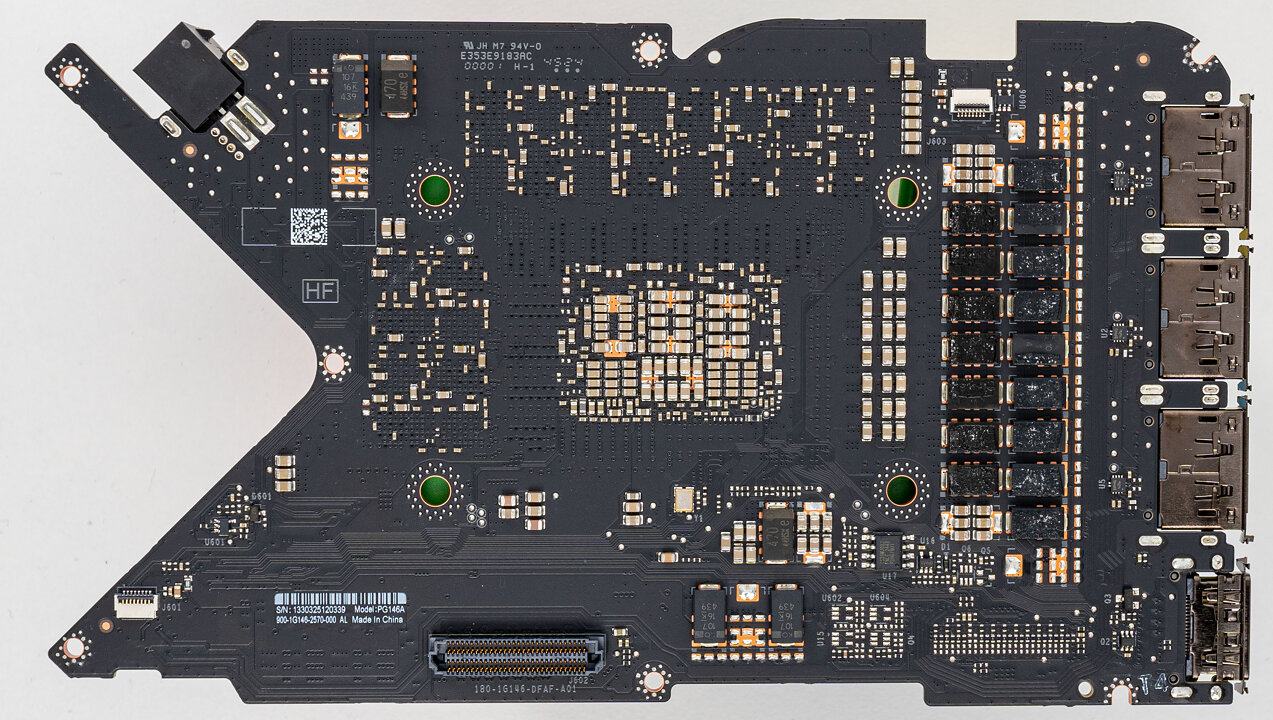
High-resolution versions are also available (front, back).
Circuit Board (PCB) Analysis
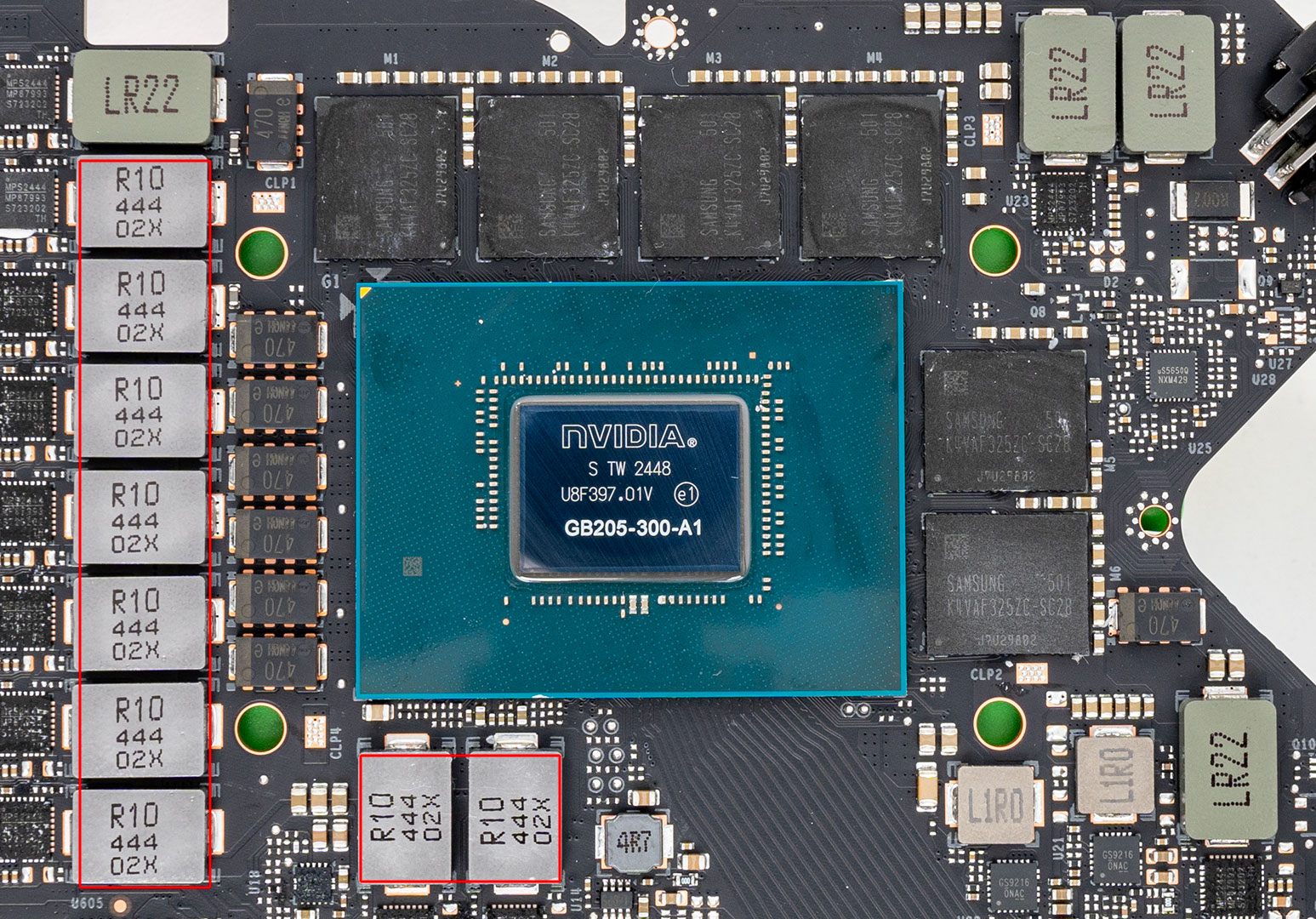
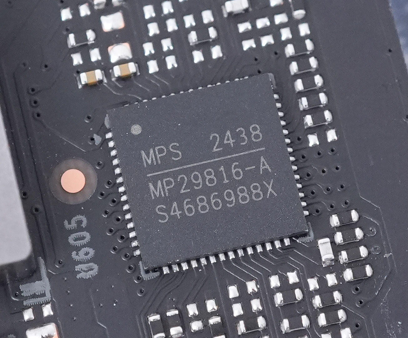
A 9-phase VRM powers the GPU, highlighted in the red rectangles above. These are controlled by a Monolithic Power Systems MP29816 controller.
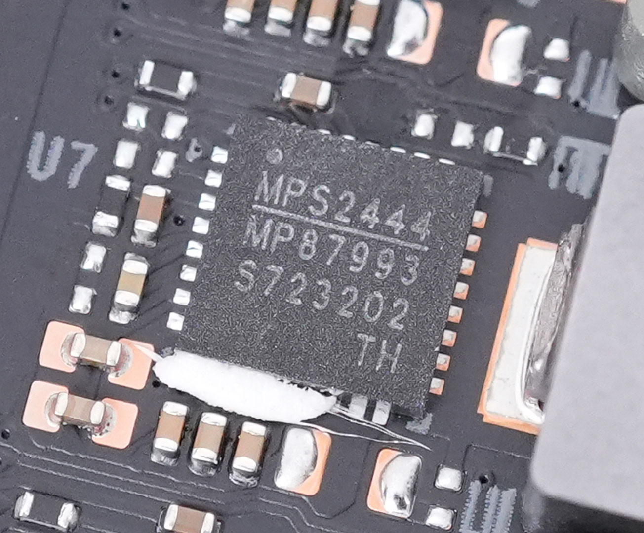
All GPU power phases use Monolithic MPS MP87993 DrMOS. These are new, we don't know their current rating. The "9" could suggest 90 A.
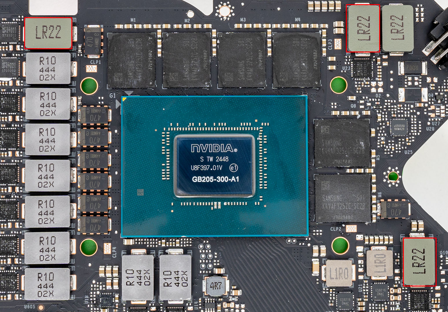
Powering the six GDDR7 memory chips is a 3-phase VRM driven by the same Monolithic MP29816 controller as the GPU VRM.

Just like GPU, the memory is handled by Monolithic MP87993 DrMOS chips.
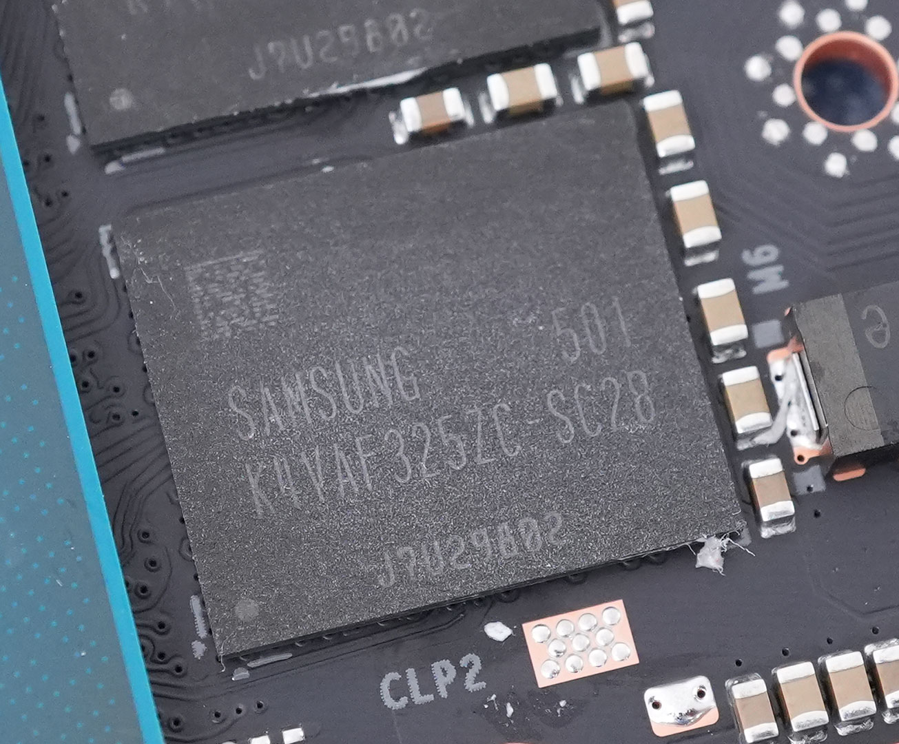
The GDDR7 memory chips are made by Samsung, and bear the model number K4VAF325ZC-SC28, they are rated for 28 Gbps.

The NVIDIA GB205 GPU at the heart of the GeForce RTX 5070 is much smaller than the chip used on the RTX 5080 and RTX 5090. It is fabricated using a 5 nanometer "NVIDIA 4N" process at TSMC Taiwan (same process as Ada). The die measures 263 mm², and comes with a transistor count of 31.1 billion.
Mar 5th, 2025 23:32 EST
change timezone
Latest GPU Drivers
New Forum Posts
- Get 9070 or 9070 XT (9)
- [Intel AX1xx/AX2xx/AX4xx/AX16xx/BE2xx/BE17xx] Intel Modded Wi-Fi Driver with Intel® Killer™ Features (283)
- Rare GPUs / Unreleased GPUs (2038)
- Optical mouse switch (3)
- Is the graphics card bios changed or normal? (7)
- Windows 11 General Discussion (5821)
- Was pentium 4 an over engineered CPU? (120)
- RTX5000 Series Owners Club (147)
- Anyone with true HDDs still around here? (296)
- PC Audio Speakers Amp/DAC/Receiver/other options? (1)
Popular Reviews
- Sapphire Radeon RX 9070 XT Nitro+ Review - Beating NVIDIA
- NVIDIA GeForce RTX 5070 Founders Edition Review
- ASUS Radeon RX 9070 TUF OC Review
- AMD Radeon RX 9070 Series Technical Deep Dive
- EIZO FlexScan EV4340X Review - A Multitasking Powerhouse
- RAWM ES21M Review
- ASUS GeForce RTX 5070 Ti TUF OC Review
- AMD Ryzen 7 9800X3D Review - The Best Gaming Processor
- MSI GeForce RTX 5070 Ti Vanguard SOC Review
- MSI GeForce RTX 5070 Ti Ventus 3X OC Review
Controversial News Posts
- NVIDIA GeForce RTX 50 Cards Spotted with Missing ROPs, NVIDIA Confirms the Issue, Multiple Vendors Affected (513)
- AMD Plans Aggressive Price Competition with Radeon RX 9000 Series (277)
- AMD Radeon RX 9070 and 9070 XT Listed On Amazon - One Buyer Snags a Unit (261)
- AMD Mentions Sub-$700 Pricing for Radeon RX 9070 GPU Series, Looks Like NV Minus $50 Again (248)
- NVIDIA Investigates GeForce RTX 50 Series "Blackwell" Black Screen and BSOD Issues (244)
- AMD RDNA 4 and Radeon RX 9070 Series Unveiled: $549 & $599 (241)
- AMD Radeon RX 9070 and 9070 XT Official Performance Metrics Leaked, +42% 4K Performance Over Radeon RX 7900 GRE (195)
- AMD Radeon RX 9070-series Pricing Leaks Courtesy of MicroCenter (158)