 23
23
Samsung 980 Pro 1 TB SSD Review - MLC No More
(23 Comments) »Introduction
As one of the world leaders in digital technology, Samsung pretty much makes any type of electronic device you can think of. Their products are used by millions of people around the world.
Being a leader in DRAM and flash memory production, it comes as no surprise that they are also a huge player in the SSD business. Their EVO and PRO Series SSDs are highly popular among upgraders, system builders, and enthusiasts.

Today, we're reviewing the Samsung 980 Pro SSD, which is a high-end M.2 NVMe drive that introduces support for the PCI-Express 4.0 interface. Internally, the Samsung 980 Pro uses Samsung's new eight-channel "Elpis" controller. Everything on the 980 Pro is produced by Samsung—the flash chips are their V-NAND v6, which uses between 110 and 136 layers of TLC. A DRAM chip is also included—it provides 1 GB of storage for the mapping tables of the SSD.
Samsung offers the 980 Pro in capacities of 250 GB ($90), 500 GB ($135), 1 TB ($230), and 2 TB ($460). Endurance for these models is set to 150 TBW, 300 TBW, 600 TBW, and 1200 TBW respectively. Samsung provides a five-year warranty for the 980 Pro.
| Specifications: Samsung 980 Pro 1 TB SSD | |
|---|---|
| Brand: | Samsung |
| Model: | MZ-V8P1T0BW |
| Capacity: | 1000 GB (931 GB usable) 24 GB additional overprovisioning |
| Controller: | Samsung Elpis S4LV003 |
| Flash: | Samsung 110 to 136-layer 3D TLC V-NAND v6 K9DUGY8J5C-DCK0 |
| DRAM: | 1x 1 GB Samsung LPDDR4 K4F8E3D4HF-BGCH |
| Endurance: | 600 TBW |
| Form Factor: | M.2 2280 |
| Interface: | PCIe Gen 4 x4, NVMe 1.3c |
| Device ID: | Samsung SSD 980 PRO 1TB |
| Firmware: | 2B2QGXA7 |
| Warranty: | Five years |
| Price at Time of Review: | $215 / 22 cents per GB |
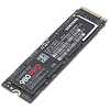
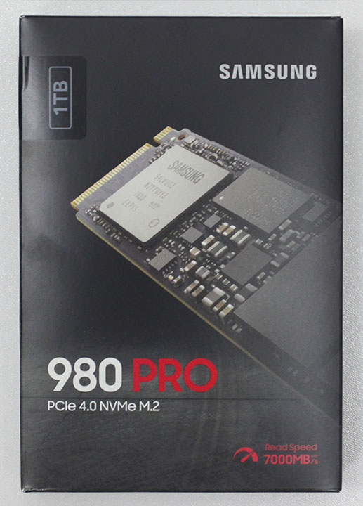
Packaging

The Drive
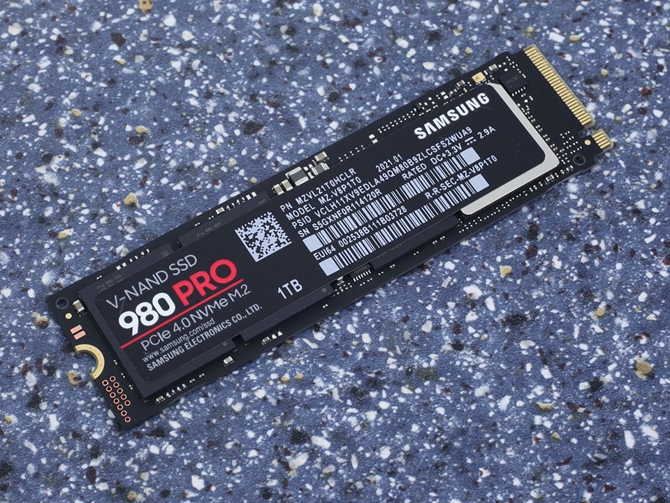

The drive uses the M.2 2280 form factor, which makes it 22 mm wide and 80 mm long.

While most other M.2 NVMe SSDs transfer data over the PCI-Express 3.0 x4 interface, the Samsung 980 Pro connects to the host system over a PCI-Express 4.0 x4 interface, which doubles the theoretical bandwidth.

On the PCB, you'll find the controller, two flash chips, and one DRAM chip; the other side of the PCB is empty.

Samsung has put a little copper foil on the back of the SSD it calls "a heat spreader label to deliver effective thermal control of the NAND chip." Yeah, not really, I doubt it makes any significant difference. It certainly doesn't have much thermal capacity simply because it has so little mass. Also, the hottest component of the drive is the controller chip, not the flash, so the label isn't positioned correctly.
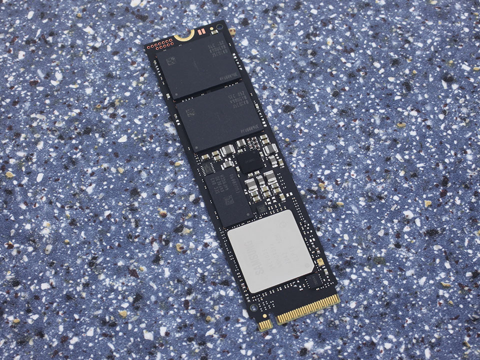
Chip Component Analysis

This is Samsung's new PCIe Gen 4 controller called "Elpis." It is produced on a 8 nm production process in Samsung's foundries, same as NVIDIA's Ampere GPUs. Compared to previous controllers, Elpis can process 128 queues at the same time (Phoenix had 32, UBX only 8).

The two flash chips are Samsung TLC V-NAND v6, which has between 110 and 136 layers. Each chip has a capacity of 512 GB.
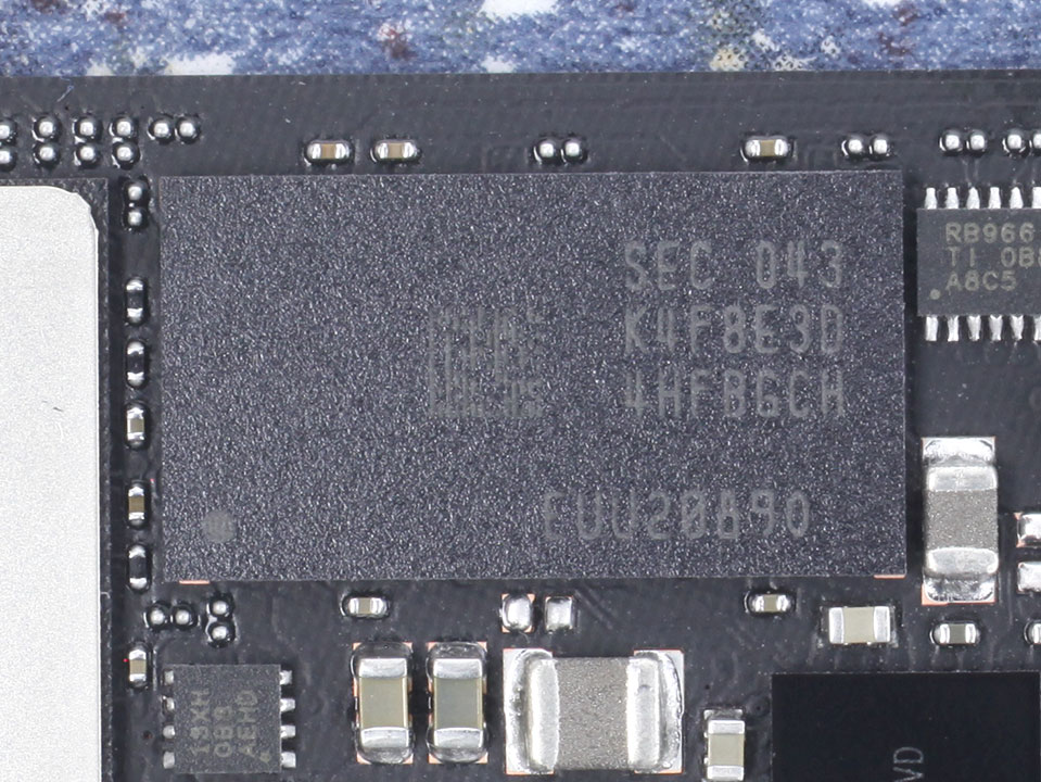
A Samsung LPDDR4 chip provides 1 GB of fast DRAM storage for the controller to store the mapping tables.
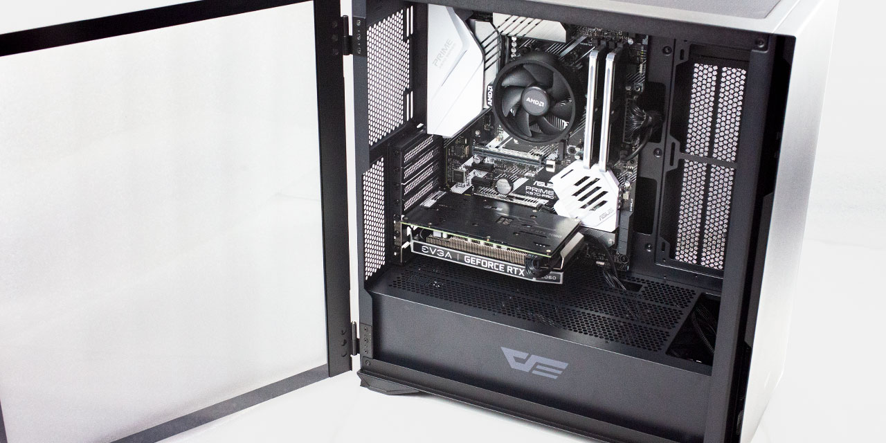
Test Setup
| Test System SSD 2021 | |
|---|---|
| Processor: | AMD Ryzen 3 3300X @ 4.3 GHz Zen 2, 16 MB Cache |
| Motherboard: | ASUS Prime X570-Pro BIOS 2606 / AGESA 1.0.8.0 |
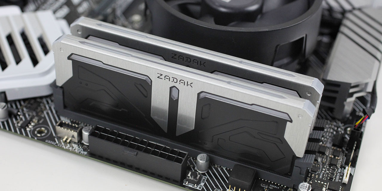
| Memory: | Zadak Spark RGB, 16 GB DDR4 @ 3200 MHz 16-18-18-38 |
| Graphics: | EVGA GeForce RTX 2060 KO 6 GB |
| Case: | DarkFlash DLX22 |
| Operating System: | Windows 10 Professional 64-bit Version 2004 (May 2020 Update) |
| Drivers: | AMD Chipset: 2.07.14.327 NVIDIA: 452.06 WHQL |


Our Patreon Silver Supporters can read articles in single-page format.
Mar 28th, 2025 22:45 EDT
change timezone
Latest GPU Drivers
New Forum Posts
- Future-proofing my OLED (54)
- Problem with Trottlestop and HWINFO64 on MSI Raider 18 (32)
- 9070 XT - 2x HDMI high refresh displays (144 and 120 Hz) not working (82)
- Issues with RTX4090 FE waterblock (Bitspower) (13)
- Dell Workstation Owners Club (3311)
- Post Your TIMESPY, PCMARK10 & FIRESTRIKE SCORES! (2019) (278)
- Solidigm NVMe Custom Modded Driver for All NVMe Brands SSDs & Any NVMe SSDs (225)
- DTS DCH Driver for Realtek HDA [DTS:X APO4 + DTS Interactive] (2119)
- [Intel AX1xx/AX2xx/AX4xx/AX16xx/BE2xx/BE17xx] Intel Modded Wi-Fi Driver with Intel® Killer™ Features (299)
- WX9100 Power mods - help w/ powerplay tables (119)
Popular Reviews
- Sapphire Radeon RX 9070 XT Pulse Review
- Samsung 9100 Pro 2 TB Review - The Best Gen 5 SSD
- Assassin's Creed Shadows Performance Benchmark Review - 30 GPUs Compared
- ASRock Phantom Gaming B850 Riptide Wi-Fi Review - Amazing Price/Performance
- be quiet! Pure Rock Pro 3 Black Review
- Sapphire Radeon RX 9070 XT Nitro+ Review - Beating NVIDIA
- ASRock Radeon RX 9070 XT Taichi OC Review - Excellent Cooling
- Pulsar Feinmann F01 Review
- Palit GeForce RTX 5070 GamingPro OC Review
- ASRock Phantom Gaming B860I Lightning Wi-Fi Review
Controversial News Posts
- AMD RDNA 4 and Radeon RX 9070 Series Unveiled: $549 & $599 (260)
- MSI Doesn't Plan Radeon RX 9000 Series GPUs, Skips AMD RDNA 4 Generation Entirely (142)
- Microsoft Introduces Copilot for Gaming (123)
- AMD Radeon RX 9070 XT Reportedly Outperforms RTX 5080 Through Undervolting (118)
- NVIDIA Reportedly Prepares GeForce RTX 5060 and RTX 5060 Ti Unveil Tomorrow (115)
- Over 200,000 Sold Radeon RX 9070 and RX 9070 XT GPUs? AMD Says No Number was Given (100)
- NVIDIA GeForce RTX 5050, RTX 5060, and RTX 5060 Ti Specifications Leak (96)
- Retailers Anticipate Increased Radeon RX 9070 Series Prices, After Initial Shipments of "MSRP" Models (90)