 22
22
ZOTAC GeForce GT 430 1 GB Review
Packaging & Contents »Introduction

Close to ten months after kicking off its DirectX 11 compliant Fermi GPU architecture, NVIDIA carefully treaded lower down the market segment order, taking its own sweet time, perhaps this is a clever strategy to make sure existing products are cleared off shelves to make room for new ones, since NVIDIA manufactures in large volumes. Today's release of the GeForce GT 430 graphics processor marks NVIDIA's entry of the Fermi architecture intro the lower-mainstream segment, the segment that holds graphics cards that are geared for GPU-enhanced everyday computing, such as smooth and clear playback of HD video, enhancing the user interface, and GPU-accelerated applications. As far as gaming goes, every game (including DirectX 11 ones) are intended to be playable at lower-resolutions (such as 1280x1024, or 1280x720) by the GeForce GT 430.
Architecture

GeForce GT 430 is based on a brand new chip by NVIDIA, codenamed GF108. The chip is built on the 40 nanometer manufacturing process, continues to be a downscaled design of the Fermi architecture. Key components are arranged in the same order and hierarchy as on every other Fermi GPU. There is one graphics processor cluster (GPC), it shares a common raster engine between two streaming multiprocessors (SMs), each SM shares an instruction cache, a dispatch, and a Polymorph Engine (that carries out several geometry-related functions), between 48 CUDA cores, that are the simplest SIMD units.
GeForce GT430 has 96 CUDA cores on the GPU, 4 raster operations processors (ROPs), and 16 texture memory units. The GPU uses a 128-bit wide memory interface. On this particular SKU there's 1 GB of DDR3 memory.
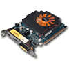
ZOTAC's GeForce GT 430 uses a custom PCB and thermal solution, while sticking to the performance specifications of the NVIDIA reference design.
| Radeon HD 5450 | GeForce 9500 GT | GeForce GT 220 | Radeon HD 5550 | GeForce GT 430 | Radeon HD 5570 | Radeon HD 4670 | GeForce GT 240 | GeForce 9600 GT | Radeon HD 5670 | |
| Shader units | 80 | 32 | 48 | 320 | 96 | 400 | 320 | 96 | 64 | 400 |
| ROPs | 4 | 8 | 8 | 8 | 4 | 8 | 8 | 8 | 16 | 8 |
| GPU | Cedar | G96 | GT216 | Redwood | GF108 | Redwood | RV730 | GT215 | G94 | Redwood |
| Transistors | 292M | 314M | 486M | 627M | 585M | 627M | 512M | 727M | 505M | 627M |
| Memory Size | 512 MB | 256 MB / 512 MB | 512 MB / 1024 MB | 1024 MB | 1024 MB | 1024 MB | 512 MB | 512 MB / 1024 MB | 512 MB | 1024 MB |
| Memory Bus Width | 64 bit | 128 bit | 128 bit | 128 bit | 128 bit | 128 bit | 128 bit | 128 bit | 256 bit | 128 bit |
| Core Clock | 650 MHz | 550 MHz | 625 MHz | 550 MHz | 700 MHz | 650 MHz | 750 MHz | 550 MHz | 650 MHz | 775 MHz |
| Memory Clock | 800 MHz | 900 MHz | 790 MHz / 1012 MHz | 1000 MHz | 900 MHz | 1000 MHz | 1000 MHz | 1700 MHz / 1000 MHz | 900 MHz | 1000 MHz |
| Price | $40 | $45 | $55 | $65 | $80 | $70 | $65 | $70 | $110 | $80 |
Apr 4th, 2025 04:51 EDT
change timezone
Latest GPU Drivers
New Forum Posts
- Why does a red screen appear when pressing F1 after updating the BIOS? (1)
- Since all gpu's models perform the same, why review dozen of different models? (28)
- RX 9000 series GPU Owners Club (134)
- What's your latest tech purchase? (23467)
- AIO - 120mm cpu cooler? (44)
- Is RX 9070 VRAM temperature regular value or hotspot? (315)
- DTS DCH Driver for Realtek HDA [DTS:X APO4 + DTS Interactive] (2125)
- The TPU UK Clubhouse (26039)
- TPU's Nostalgic Hardware Club (20164)
- Mllse 6600s that are locked at 500 mhz. (7)
Popular Reviews
- DDR5 CUDIMM Explained & Benched - The New Memory Standard
- PowerColor Radeon RX 9070 Hellhound Review
- Sapphire Radeon RX 9070 XT Pulse Review
- Corsair RM750x Shift 750 W Review
- Pwnage Trinity CF Review
- Sapphire Radeon RX 9070 XT Nitro+ Review - Beating NVIDIA
- Upcoming Hardware Launches 2025 (Updated Apr 2025)
- SilverStone Lucid 04 Review
- Palit GeForce RTX 5070 GamingPro OC Review
- AMD Ryzen 7 9800X3D Review - The Best Gaming Processor
Controversial News Posts
- MSI Doesn't Plan Radeon RX 9000 Series GPUs, Skips AMD RDNA 4 Generation Entirely (146)
- Microsoft Introduces Copilot for Gaming (124)
- AMD Radeon RX 9070 XT Reportedly Outperforms RTX 5080 Through Undervolting (119)
- NVIDIA Reportedly Prepares GeForce RTX 5060 and RTX 5060 Ti Unveil Tomorrow (115)
- Over 200,000 Sold Radeon RX 9070 and RX 9070 XT GPUs? AMD Says No Number was Given (100)
- NVIDIA GeForce RTX 5050, RTX 5060, and RTX 5060 Ti Specifications Leak (96)
- Retailers Anticipate Increased Radeon RX 9070 Series Prices, After Initial Shipments of "MSRP" Models (90)
- Nintendo Switch 2 Launches June 5 at $449.99 with New Hardware and Games (90)