 9
9
Zotac GeForce RTX 3050 Twin Edge OC Review
Test Setup »High-resolution PCB Pictures
These pictures are for the convenience of volt modders and people who would like to see all the finer details on the PCB. Feel free to link back to us and use these in your articles, videos or forum posts.High-res versions are also available (front, back).
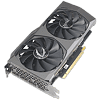
Circuit Board (PCB) Analysis
The GPU VRM is a four phase-design controlled by a Richtek RT8848A controller.
For the GPU voltage, OnSemi NCP252160 DrMOS are used; they are rated for up to 60 A output current.
The memory VRM is single-phase and managed by a uPI uP1666Q controller.
For memory, M3828N MOSFETs are used.
The GDDR6 memory chips are made by Micron and carry the model number D9ZPM, which decodes to MT61K512M32KPA-14:C. They are specified to run at 1750 MHz (14 Gbps GDDR6 effective).
NVIDIA's GA106 graphics processor is made using Samsung's 8 nanometer node and has a transistor count of 12 billion with a die size of 276 mm².
Dec 22nd, 2024 09:04 EST
change timezone
Latest GPU Drivers
New Forum Posts
- What do you do for a living? (392)
- What is the best pc case? (12)
- The Official Linux/Unix Desktop Screenshots Megathread (757)
- Intel ARC Firmware Compilation Matrix (21)
- Ghetto Mods (4521)
- Upgrade advice please (4)
- How many are using 24h2? Problems still? (78)
- Gigabyte am5 motherboard ddr5 not posting when rebooting (116)
- Best time to sell your used 4090s is now. (132)
- ASUS ROG Strix X670E-I m.2 heatsink (1)
Popular Reviews
- Arrow Lake Retested with Latest 24H2 Updates and 0x114 Microcode
- Team Group T-FORCE Dark AirFlow I SSD Cooler Review
- Intel Arc B580 Review - Excellent Value
- Montech MKey PRO Wireless Mechanical Keyboard Review
- DUNU DK3001BD In-Ear Monitors Review - Brain Dance Time!
- AMD Ryzen 7 9800X3D Review - The Best Gaming Processor
- ASRock Arc B580 Steel Legend Review
- Dangbei Atom ALPD Laser Projector Review
- FiiO BTR17 Portable Bluetooth DAC and Headphones Amplifier Review
- Endgame Gear XM2w 4K Review
Controversial News Posts
- Intel CEO Pat Gelsinger Retires, Company Appoints two Interim co-CEOs (217)
- AMD Radeon RX 8800 XT RDNA 4 Enters Mass-production This Month: Rumor (215)
- 32 GB NVIDIA RTX 5090 To Lead the Charge As 5060 Ti Gets 16 GB Upgrade and 5060 Still Stuck With Last-Gen VRAM Spec (160)
- NVIDIA GeForce RTX 5070 Ti Leak Tips More VRAM, Cores, and Power Draw (159)
- AMD Radeon RX 8800 XT Reportedly Features 220 W TDP, RDNA 4 Efficiency (123)
- Intel 18A Process Node Clocks an Abysmal 10% Yield: Report (90)
- NVIDIA Blackwell RTX and AI Features Leaked by Inno3D (87)
- Microsoft Loosens Windows 11 Install Requirements, TPM 2.0 Not Needed Anymore (83)


