 450
450
AMD Radeon RX 480 8 GB Review
The Card »Architecture
At the heart of the Radeon RX 480 is the new "Ellesmere" (Polaris 10) GPU built on the 14 nanometer silicon fab process by Samsung and GlobalFoundries. The wafers are made in Upstate New York, USA, and are then bumped and packaged at a facility in Taiwan to be sent to the various graphics card manufacturers located there and across the straits.This GPU is based on AMD's fourth generation Graphics CoreNext architecture codenamed "Polaris." According to AMD, Compute Units (CUs) based on Polaris are 15% more efficient at number-crunching than CUs based on the preceding Graphics CoreNext 1.2 architecture (R9 Fury, R9 380X). Pay attention to the numbers here. While the number-crunching machinery is 15% more efficient, the chip overall is claimed to have a 2.5x leap in energy-efficiency over the previous generation. This is because AMD is cashing in on the immediate gains a new silicon fab process brings to the table, the 14 nm FinFET process in this case, to increase transistor counts and clock speeds.
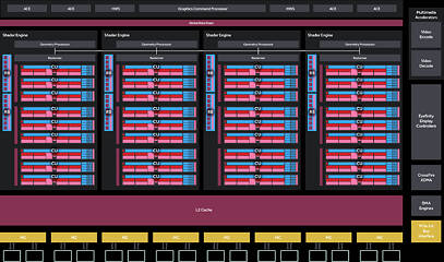
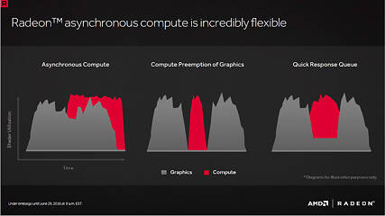
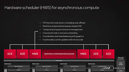
The component hierarchy in the Polaris 10 "Ellesmere" silicon is similar to older-generation chips, although each of the components received major updates. We begin with the chip featuring two hardware schedulers and the introduction of dedicated real-time asynchronous compute with spatial and temporal scheduling. The chip features four async compute engines (ACEs). AMD optimized the async compute engine with new quick-response queue tech.
There's a design focus on stepping up geometry processing performance and blunting the brute-tessellation advantage NVIDIA traditionally enjoyed over AMD. For a chip of this segment, Polaris 10 features four independent geometry processors. Their functionality is upgraded over the previous generation, featuring a primitive discard accelerator which culls (discards) triangles in the pipeline with zero area or no inclusive sample points. The geometry engine now features a tiny cache called the Index Cache, which cushions small instanced geometry and reduces data movement, improving primitive throughput during instancing.
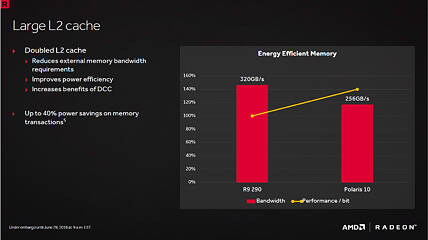
The Polaris 10 silicon features 36 Compute Units (CUs), spread across four shader engines, each with a dedicated geometry processor, a raster engine, and two render backends. The four shader engines are supported by a large 2 MB L2 cache, which acts as the town-square for the various key components of the GPU.
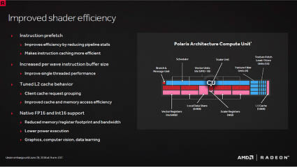
Most of the architecture-specific innovations are centered on the CU, which now features a hardware instruction prefetcher, a larger instruction buffer, and native half-precision (FP16/Int16) support, which should reliably crunch numbers for gaming applications with significantly reduced memory and register footprints while lowering power execution. Altogether, the "Polaris" CU is claimed to have up to 15% higher performance than CUs based on the GCN 1.1 architecture (R9 390X). Each CU features 64 stream processors, and so the 36 CUs amount to 2,304 stream processors. The Radeon RX 480 maxes out all CUs physically present on the chip. In summary, the Polaris 10 chip features 2,304 stream processors, 144 TMUs, and 32 ROPs.
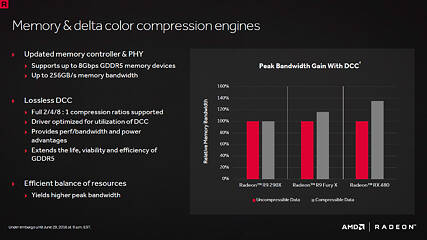
The Polaris 10 chip features a 256-bit wide GDDR5 memory interface, supporting 8 Gbps memory chips in sizes of up to 8 GB. The actual memory bandwidth of this interface, at its given clock speeds, is rated at up to 256 GB/s, although its effective bandwidth could be higher thanks to an updated lossless delta color compression (DCC) tech with full 2/4/8:1 compression ratios. AMD claims that its new gen DCC tech can provide an effective bandwidth uplift of a staggering 30 percent.
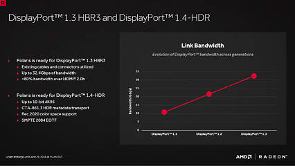
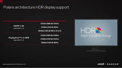
The multimedia accelerators receive a major update, now supporting H.265 Main10 decode hardware acceleration and 4K60 HEVC encode hardware acceleration. The other components with big updates are the display controllers, which now support DisplayPort 1.4 (DP 1.3 HBR3 and DP 1.4 HDR) and HDMI 2.0b. FreeSync is supported over both DP and HDMI. Resolutions as high as 5K60, 10-bit 4K96 HDR, and 4K120 SDR are supported.
Dec 22nd, 2024 18:50 EST
change timezone
Latest GPU Drivers
New Forum Posts
- Free Games Thread (4293)
- USB4 cases and docks (3)
- Rattle sound on 7800XT (25)
- How many are using 24h2? Problems still? (81)
- Unlock the shaders - AMD Radeon RX 560D (331)
- Question HDD + case + eject windows (40)
- Bricked asus rx 570 8GB :( (16)
- Upgrade or Complete Upgrade? (11)
- Throttling Asus ROG Strix (14900HX & 4070) (20)
- How to install nvidia driver for rtx3080 on windows 1709? (69)
Popular Reviews
- Arrow Lake Retested with Latest 24H2 Updates and 0x114 Microcode
- Team Group T-FORCE Dark AirFlow I SSD Cooler Review
- Intel Arc B580 Review - Excellent Value
- Montech MKey PRO Wireless Mechanical Keyboard Review
- DUNU DK3001BD In-Ear Monitors Review - Brain Dance Time!
- AMD Ryzen 7 9800X3D Review - The Best Gaming Processor
- ASRock Arc B580 Steel Legend Review
- Dangbei Atom ALPD Laser Projector Review
- FiiO BTR17 Portable Bluetooth DAC and Headphones Amplifier Review
- Endgame Gear XM2w 4K Review
Controversial News Posts
- Intel CEO Pat Gelsinger Retires, Company Appoints two Interim co-CEOs (217)
- AMD Radeon RX 8800 XT RDNA 4 Enters Mass-production This Month: Rumor (215)
- 32 GB NVIDIA RTX 5090 To Lead the Charge As 5060 Ti Gets 16 GB Upgrade and 5060 Still Stuck With Last-Gen VRAM Spec (165)
- NVIDIA GeForce RTX 5070 Ti Leak Tips More VRAM, Cores, and Power Draw (160)
- AMD Radeon RX 8800 XT Reportedly Features 220 W TDP, RDNA 4 Efficiency (123)
- Intel 18A Process Node Clocks an Abysmal 10% Yield: Report (90)
- NVIDIA Blackwell RTX and AI Features Leaked by Inno3D (87)
- Microsoft Loosens Windows 11 Install Requirements, TPM 2.0 Not Needed Anymore (83)
