News Posts matching #3 nm

Return to Keyword Browsing

Samsung Electronics Announces Third Quarter 2023 Results

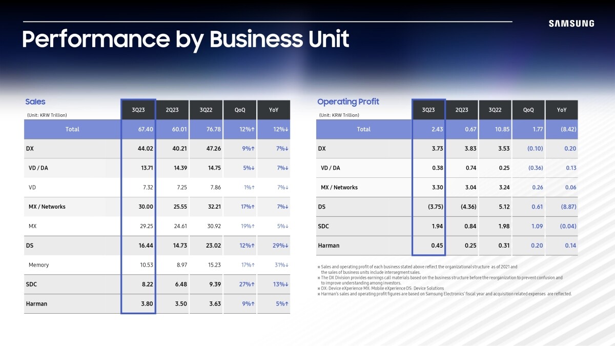
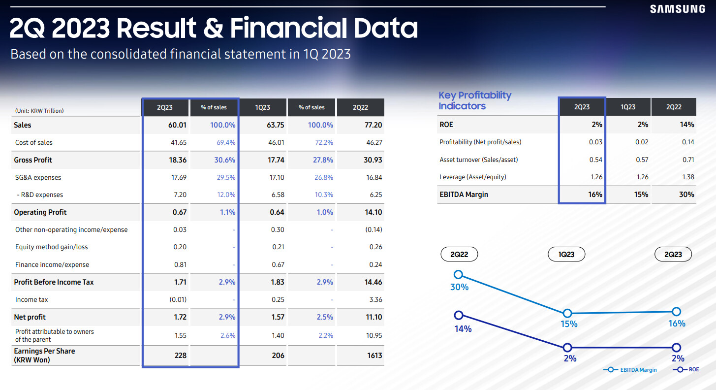
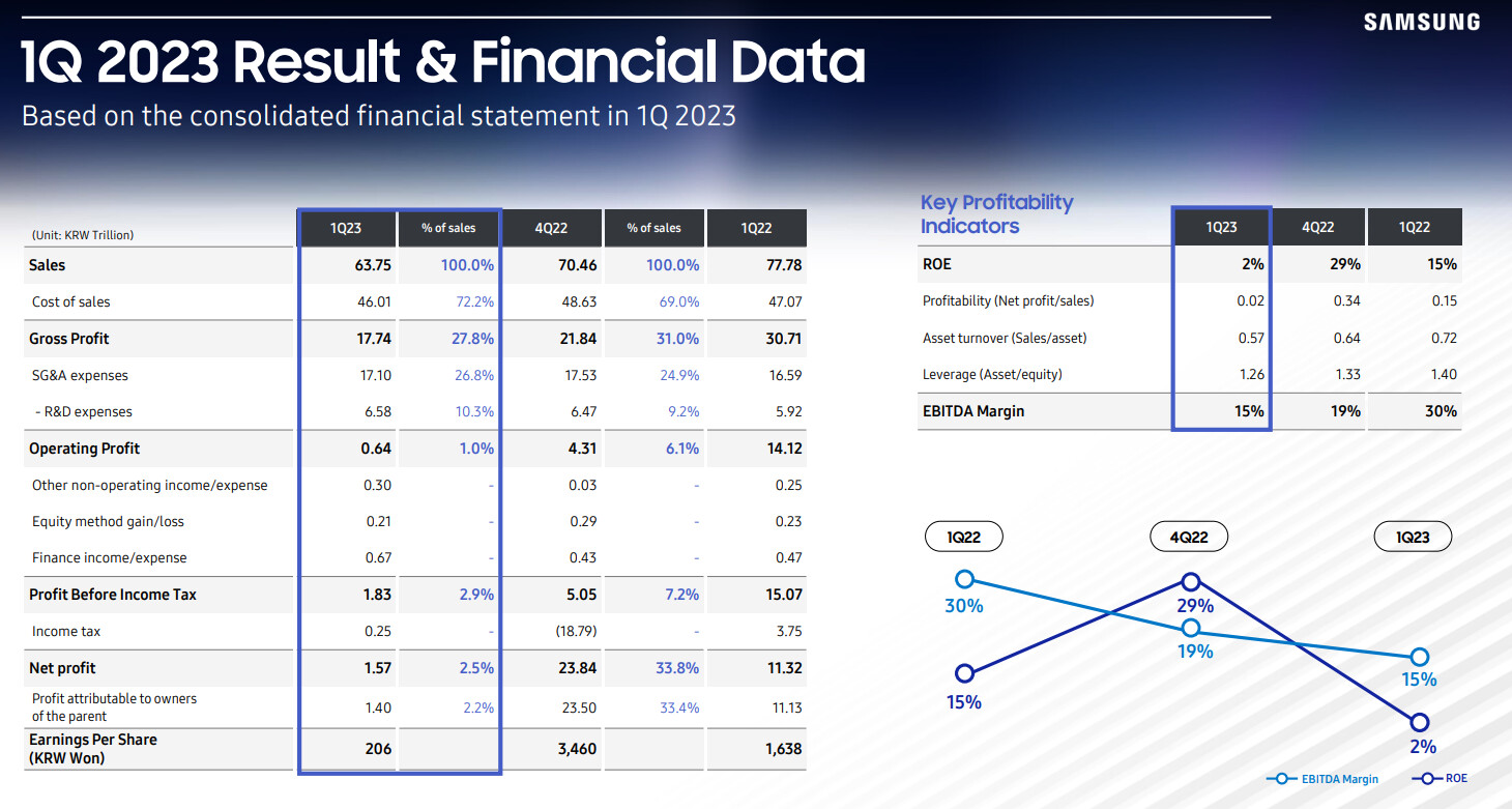
Samsung Electronics today reported financial results for the third quarter ended September 30, 2023. Total consolidated revenue was KRW 67.40 trillion, a 12% increase from the previous quarter, mainly due to new smartphone releases and higher sales of premium display products. Operating profit rose sequentially to KRW 2.43 trillion based on strong sales of flagship models in mobile and strong demand for displays, as losses at the Device Solutions (DS) Division narrowed.

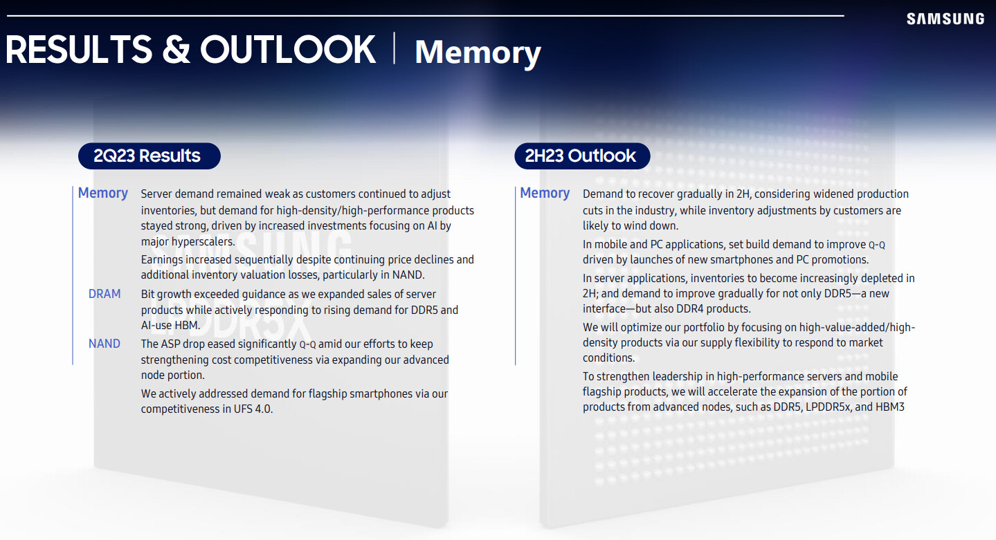
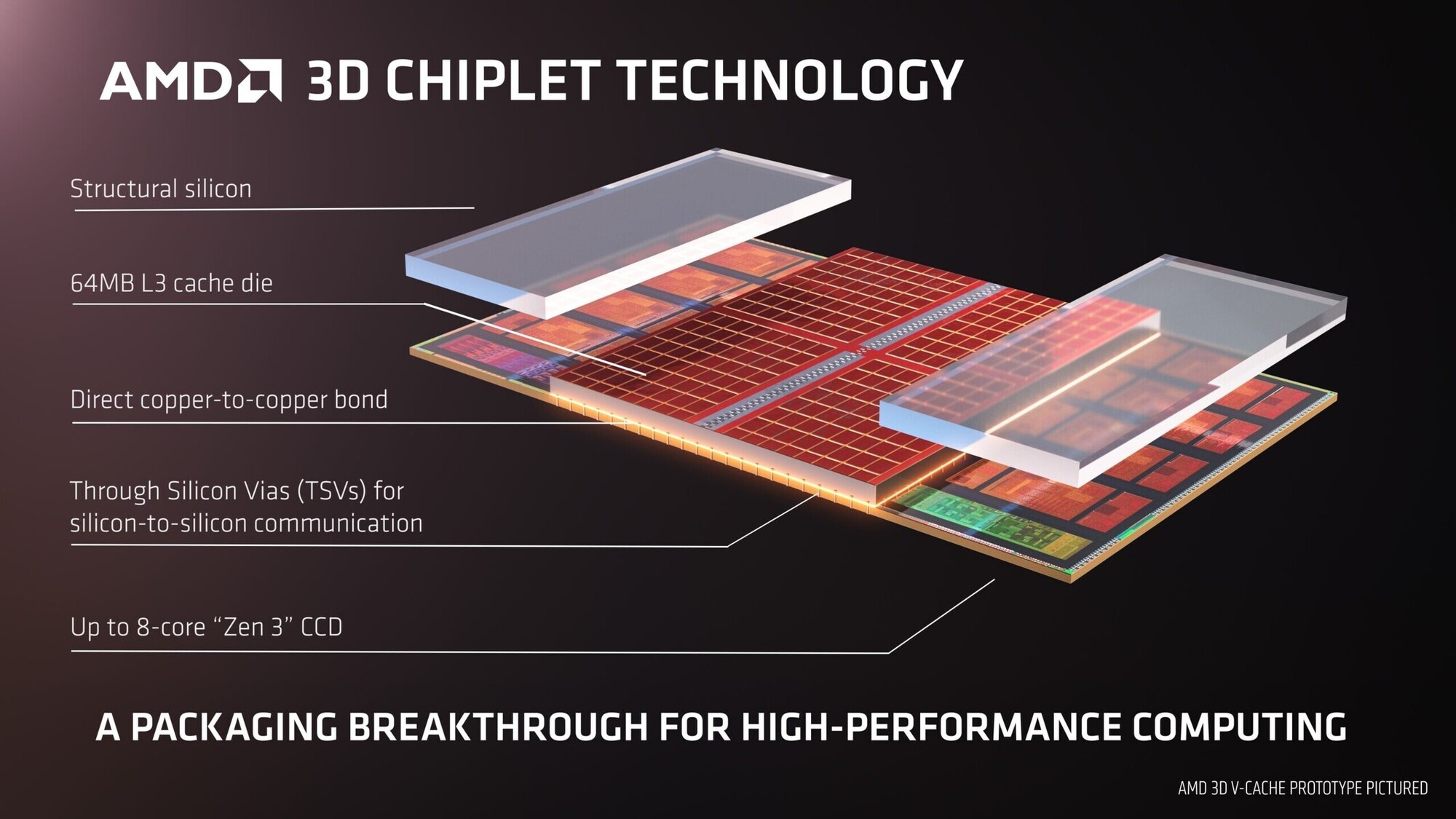
The Memory Business reduced losses sequentially as sales of high valued-added products and average selling prices somewhat increased. Earnings in system semiconductors were impacted by a delay in demand recovery for major applications, but the Foundry Business posted a new quarterly high for new backlog from design wins. The mobile panel business reported a significant increase in earnings on the back of new flagship model releases by major customers, while the large panel business narrowed losses in the quarter. The Device eXperience (DX) Division achieved solid results due to robust sales of premium smartphones and TVs. Revenue at the Networks Business declined in major overseas markets as mobile operators scaled back investments.

Samsung and TSMC Reportedly Struggling with 3 nm Yields

According to Korean business news publication ChosunBiz, both Samsung and TSMC are struggling with their 3 nm node yields. The two companies have different approaches to their 3 nm nodes, with Samsung using GAA FET (Gate All Around), whereas TSMC is continuing with its FinFET technology. That said, TSMC has at least five known 3 nm nodes, of which two should be in production by now, assuming N3E has proved to be reliable enough to kick off. Samsung on the other hand has three known 3 nm nodes, with only one in production so far, called 3GAE.

ChosunBiz reports that neither company is getting the kind of yields that you'd expect from a node that should have been in volume production for around a year by now, with Samsung apparently being somewhat better than TSMC. At 60 and 50 percent respectively, neither Samsung nor TSMC are anywhere near decent yields. Anything below 70 percent is considered very poor and even the 60 percent claim in Samsungs case, is apparently limited to some kind of Chinese mining ASIC and doesn't include the SRAM you find in most modern processors. ChosunBiz also mentions a source familiar with Samsung's foundry business who mentions a yield closer to 50 percent for the company. The same source also mentions that Samsung needs to reach at least 70 percent yield to be able to attract major customers to its 3 nm node.

AMD Zen 5 Microarchitecture Referenced in Leaked Slides

A couple of slides from AMD's internal presentation were leaked to the web by Moore's Law is Dead, referencing what's allegedly the next-generation "Zen 5" microarchitecture. Internally, the performance variant of the "Zen 5" core is referred to as "Nirvana," and the CCD chiplet (CPU core die) based on "Nirvana" cores, is codenamed "Eldora." These CCDs will make up either the company's Ryzen "Granite Ridge" desktop processors, or EPYC "Turin" server processors. The cores themselves could also be part of the company's next-generation mobile processors, as part of heterogenous CCXs (CPU core complex), next to "Zen 5c" low-power cores.

In broad strokes, AMD describes "Zen 5" as introducing a 10% to 15% IPC increase over the current "Zen 4." The core will feature a larger 48 KB L1D cache, compared to the current 32 KB. As for the core itself, it features an 8-wide dispatch from the micro-op queue, compared to the 6-wide dispatch of "Zen 4." The integer execution stage gets 6 ALUs, compared to the current 4. The floating point unit gets FP-512 capabilities. Perhaps the biggest announcement is that AMD has increased the maximum cores per CCX from 8 to 16. At this point we don't know if it means that "Eldora" CCD will have 16 cores, or whether it means that the cloud-specific CCD with 16 "Zen 5c" cores will have 16 cores within a single CCX, rather than spread across two CCXs with smaller L3 caches. AMD is leveraging the TSMC 4 nm EUV node for "Eldora," the mobile processor based on "Zen 5" could be based on the more advanced TSMC 3 nm EUV node.

NVIDIA Reportedly Selects TSMC 3 nm Process for Blackwell GB100 GPU

NVIDIA is reported to be on next year's 3 nm-class order book at TSMC, with the Blackwell GB100 data-center GPU marked down as an important production project. A DigiTimes insider piece proposes that Team Green has signed up for orders in the second half of 2024, giving TSMC some wiggle room to iron out alleged advanced packaging issues—but it is implied that Apple is already ahead in the queue. Inside sources have not spotted an Intel request for TSMC's advanced 3 nm process (still utilizing FinFET). Industry experts reckon that NVIDIA could be granted access to a customized node for its Blackwell product line, given their VIP status and special relationship with the leading Taiwanese foundry.

DigiTimes believes that the Blackwell GB100 (sporting a chiplet design) will be targeting a Q4 2024 launch window, therefore arriving before any competing next-gen technologies: "For NVIDIA, which monopolizes more than 80% of the AI GPU market, the next generation B100 will use TSMC's 3 nm...It will seize AI deployment business opportunities while the iron is hot and suppress AMD, Intel and other challengers." Team Red, MediaTek and Qualcomm could be next in the procession—it is claimed that unspecified next-gen EPYC server chips are due in 3 nm form.

TSMC Could Delay 2 nm Mass Production to 2026

According to TechNews.tw, TSMC could postpone its 2 nm semiconductor manufacturing node for 2026. If the rumors about TSMC's delayed 2 nm production schedule are accurate, the implications could reverberate throughout the semiconductor industry. TSMC's alleged hesitancy could be driven by multiple factors, including the architectural shift from FinFET to Gate-All-Around (GAA) and potential challenges related to scaling down to 2 nm. The company is a crucial player in this space, and a delay could offer opportunities for competitors like Samsung, which has already transitioned to GAA transistor architecture for its 3 nm chips. Given the massive demand for advanced nodes due to the rise of AI, IoT, and other next-gen technologies, it is surprising to hear "sluggish" demand reports.

However, it's also possible that it's too early for customers to make firm commitments for 2025 and beyond. TSMC has dismissed these rumors, stating that construction is progressing according to plan, which includes having 2 nm pilot run in 2024, and mass production in the second half of 2025.. Despite this, any delay in TSMC's roadmap could serve as a catalyst for shifts in market dynamics. Companies that rely heavily on TSMC's advanced nodes might need to reassess their timelines and strategies. Moreover, if Samsung can capitalize on this opportunity, it could somewhat level the playing field. As of now, though, it's essential to approach these rumors with caution until more concrete information becomes available.

MediaTek Successfully Develops First Chip Using TSMC's 3 nm Process, Set for Volume Production in 2024

MediaTek and TSMC today announced that MediaTek has successfully developed its first chip using TSMC's leading-edge 3 nm technology, taping out MediaTek's flagship Dimensity system-on-chip (SoC) with volume production expected next year. This marks a significant milestone in the long-standing strategic partnership between MediaTek and TSMC, with both companies taking full advantage of their strengths in chip design and manufacturing to jointly create flagship SoCs with high performance and low power features, empowering global end devices.

"We are committed to our vision of using the world's most advanced technology to create cutting edge products that improve our lives in meaningful ways," said Joe Chen, President of MediaTek. "TSMC's consistent and high-quality manufacturing capabilities enable MediaTek to fully demonstrate its superior design in flagship chipsets, offering the highest performance and quality solutions to our global customers and enhancing the user experience in the flagship market."

Top Ten Semiconductor Foundries Report a 1.1% Quarterly Revenue Decline in 2Q23, Anticipated to Rebound in 3Q23

TrendForce reports an interesting shift in the electronics landscape: dwindling inventories for TV components, along with a surging mobile repair market that's been driving TDDI demand, have sparked a smattering of urgent orders in the Q2 supply chain. These last-minute orders have served as pivotal lifelines, propping up Q2 capacity utilization and revenue for semiconductor foundries. However, the adrenaline rush from these stop-gap orders may be a short-lived phenomenon and is unlikely to be carried over into the third quarter.

On the other hand, demand for staple consumer products like smartphones, PCs, and notebooks remains sluggish, perpetuating a slump in the use of expensive, cutting-edge manufacturing processes. At the same time, traditionally stable sectors—automotive, industrial control, and servers—are undergoing inventory correction. The confluence of these trends has resulted in a sustained contraction for the world's top ten semiconductor foundries. Their global revenue declined by approximately 1.1% for the quarter, amounting to a staggering US$26.2 billion.

AMD "Navi 4C" GPU Detailed: Shader Engines are their own Chiplets

"Navi 4C" is a future high-end GPU from AMD that will likely not see the light of day, as the company is pivoting away from the high-end GPU segment with its next RDNA4 generation. For AMD to continue investing in the development of this GPU, the gaming graphics card segment should have posted better sales, especially in the high-end, which it didn't. Moore's Law is Dead scored details of what could have been a fascinating technological endeavor for AMD, in building a highly disaggregated GPU.

AMD's current "Navi 31" GPU sees a disaggregation of the main logic components of the GPU that benefit from the latest 5 nm foundry node to be located in a central Graphics Compute Die; surrounded by up to six little chiplets built on the older 6 nm foundry node, which contain segments of the GPU's Infinity Cache memory, and its memory interface—hence the name memory cache die. With "Navi 4C," AMD had intended to further disaggregate the GPU, identifying even more components on the GCD that can be spun out into chiplets; as well as breaking up the shader engines themselves into smaller self-contained chiplets (smaller dies == greater yields and lower foundry costs).

Samsung Electronics Announces Second Quarter 2023 Results

Samsung Electronics today reported financial results for the second quarter ended June 30, 2023. The Company posted KRW 60.01 trillion in consolidated revenue, a 6% decline from the previous quarter, mainly due to a decline in smartphone shipments despite a slight recovery in revenue of the DS (Device Solutions) Division. Operating profit rose sequentially to KRW 0.67 trillion as the DS Division posted a narrower loss, while Samsung Display Corporation (SDC) and the Digital Appliances Business saw improved profitability.

The Memory Business saw results improve from the previous quarter as its focus on High Bandwidth Memory (HBM) and DDR5 products in anticipation of robust demand for AI applications led to higher-than-guided DRAM shipments. System semiconductors posted a decline in profit due to lower utilization rates on weak demand from major applications.

Samsung's 3 nm GAA Process Identified in a Crypto-mining ASIC Designed by China Startup MicroBT

Semiconductor industry research firm TechInsights said it has found that Samsung's 3 nm GAA (gate-all-around) process has been incorporated into the crypto miner ASIC (Whatsminer M56S++) from a Chinese manufacturer, MicroBT. In a Disruptive Technology Event Brief exclusively provided to DIGITIMES Asia, TechInsights points out that the significance of this development lies in the commercial utilization of GAA technology, which facilitates the scaling of transistors to 2 nm and beyond. "This development is crucial because it has the potential to enhance performance, improve energy efficiency, keep up with Moore's Law, and enable advanced applications," said TechInsights, identifying the MicroBT ASIC chip the first commercialized product using GAA technology in the industry.

But this would also reveal that Samsung is the foundry for MicroBT, using the 3 nm GAA process. DIGITIMES Research semiconductor analyst Eric Chen pointed out that Samsung indeed has started producing chips using the 3 nm GAA process, but the capacity is still small. "Getting revenues from shipment can be defined as 'commercialization', but ASIC is a relatively simple kind of chip to produce, in terms of architecture."

Samsung Claims Higher 3 nm Yields than TSMC

Competition between Samsung and TSMC in the 4 nm and 3 nm foundry process markets is about to heat up, with the Korean foundry claiming yields competitive to those of TSMC, according to a report in the Kukmin Ilbo, a Korean daily newspaper. 4 nm is the final silicon fabrication process to use the FinFET technology that powered nodes ranging between 16 nm to 4 nm. Samsung Foundry is claiming 4 nm wafer yields of 75%, against the 80% yields figure put out by TSMC. 4 nm powers several current-generation mobile SoCs, PC processors, and more importantly, the GPUs driving the AI gold-rush.

Things get very interesting with 3 nm, the node that debuts GAA-FET (gates all around FET) technology. Here, Samsung claims to offer higher yields than TSMC, with its 3 nm GAA node clocking 60% yields, against 55% put out by TSMC. Samsung was recently bitten by a scandal where its engineers allegedly falsified yields figures to customers to score orders, which had a cascading effect on the volumes and competitiveness of their customers. We're inclined to think that Samsung has taken lessons and is more careful with the yields figures being reported in the press. Meanwhile, Intel Foundry Services competes with the Intel 3 node, which is physically 7 nm FinFET, but with electrical characteristics comparable to those of 3 nm.

TSMC Said to Start Construction of 1.4 nm Fab in 2026

According to Taiwanese media, TSMC will start production of its first 1.4 nm fab in 2026, with chip production in the fab said to start sometime in 2027 or 2028. The new fab will be located in Longtan Science Park outside of Hsinchu in Taiwan, where many of TSMC's current fabs are located. TSMC is currently constructing a 2 nm and below node R&D facility at a nearby plot of land to where the new fab is expected to be built. This facility is expected to be finished in 2025 and TSMC has been allocated a total area of just over 158 hectares of land for future expansion in the area.

In related news, TSMC is expected to be charging US$25,000 per 2 nm GAA wafer, which is an increase of about a fifth compared to its 3 nm wafers which are going for around US$20,000. This is largely due to the nodes being fully booked and TSMC being able to charge a premium for its cutting edge nodes. TSMC is also expanding in CoWoS packaging facilities due to increased demand from both AMD and NVIDIA for AI related products. Currently TSMC is said to be able to output 12,000 CoWoS wafers per month and this is twice as much as last year, yet TSMC is unable to meet demand from its customers.

Samsung Electronics Unveils Foundry Vision in the AI Era

Samsung Electronics, a world leader in advanced semiconductor technology, today announced its latest foundry technology innovations and business strategy at the 7th annual Samsung Foundry Forum (SFF) 2023. Under the theme "Innovation Beyond Boundaries," this year's forum delved into Samsung Foundry's mission to address customer needs in the artificial intelligence (AI) era through advanced semiconductor technology.

Over 700 guests, from customers and partners of Samsung Foundry, attended this year's event, of which 38 companies hosted their own booths to share the latest technology trends in the foundry industry.

Top 10 Foundries Report Nearly 20% QoQ Revenue Decline in 1Q23, Continued Slide Expected in Q2

TrendForce reports that the global top 10 foundries witnessed a significant 18.6% QoQ decline in revenue during the first quarter of 2023. This decline—amounting to approximately US$27.3 billion—can be attributed to sustained weak end-market demand and the compounded effects of the off-peak season. The rankings also underwent notable changes, with GlobalFoundries surpassing UMC to secure the third position, and Tower Semiconductor surpassing PSMC and VIS to claim the seventh spot.

Declining capacity utilization rate and shipment volume contribute to widened revenue decline
The revenue decline in Q1 was primarily influenced by declining capacity utilization rates and shipment volume across the top 10 foundries. For instance, TSMC generated US$16.74 billion in revenue—marking a 16.2% QoQ drop in revenue. Weakened demand for mainstream applications such as laptops and smartphones led to a significant decline in the utilization rates and revenue of the 7/6 nm and 5/4 nm processes, falling over 20% and 17%, respectively. While the second quarter may see temporary relief coming from rush orders, the persistently low capacity utilization rate indicates that revenue is likely to continue declining, albeit at a slower pace compared to Q1.

TSMC N3 Nodes Show SRAM Scaling is Hitting the Wall

When TSMC introduced its N3 lineup of nodes, the company only talked about the logic scaling of the two new semiconductor manufacturing steps. However, it turns out that there was a reason for it, as WikiChip confirms that the SRAM bit cells of N3 nodes are almost identical to the SRAM bit cells of N5 nodes. At TSMC 2023 Technology Symposium, TSMC presented additional details about its N3 node lineup, including logic and SRAM density. For starters, the N3 node is TSMC's "3 nm" node family that has two products: a Base N3 node (N3B) and an Enhanced N3 node (N3E). The base N3B uses a new (for TSMC) self-aligned contact (SAC) scheme that Intel introduced back in 2011 with a 22 nm node, which improves the node's yield.

Regardless of N3's logic density improvements compared to the "last-generation" N5, the SRAM density is almost identical. Initially, TSMC claimed N3B SRAM density was 1.2x over the N5 process. However, recent information shows that the actual SRAM density is merely a 5% difference. With SRAM taking a large portion of the transistor and area budget of a processor, N3B's soaring manufacturing costs are harder to justify when there is almost no area improvement. For some time, SRAM scaling wasn't following logic scaling; however, the two have now completely decoupled.

Apple M3 Pro Chip to Pack Entry-Level Configuration of 12 CPU Cores and 18 GPU Cores on TSMC 3 nm Technology

Thanks to the latest release of the Power On newsletter from Mark Gurman, we have additional information about Apple's upcoming M3 Pro chip. Currently in testing and reported on by an App Store developer, Apple is looking to upgrade the microarchitecture of the forthcoming chip and add additional cores to the system for more performance. As the report notes, the entry-level M3 Pro chip currently in testing will have 12 CPU cores, six for efficiency and six for performance tasks, with 18 graphics cores, all manufactured on TSMC's 3 nm node. The current baseline for M2 Pro is 10 CPU cores, where four are dedicated to efficiency, and six are dedicated to performance. The current generation entry-level M2 Pro also features a 16-core GPU, which is two cores fewer than the upcoming model.

Generally, the M3 Pro chip will boost integrated memory across the board, as the sample spotted in testing shows 36 GB of memory. The M2 Pro offered 32 GB in that memory tier, so a four GB increase is inbound there. Presumably, the 16 GB version (if it exists) and 64 GB version will also get memory bumps by going the M3 Pro route. Of course, we have to wait for more information as these chips become more widely available to developers.

AMD Ryzen 8000 "Granite Ridge" Zen 5 Processor to Max Out at 16 Cores

AMD's next-generation Ryzen 8000 "Granite Ridge" desktop processor based on the "Zen 5" microarchitecture, will continue to top out at 16-core/32-thread as the maximum CPU core-count possible, says a report by PC Games Hardware. The processor will retain the chiplet design of the current Ryzen 7000 "Raphael" processor, with two 8-core "Zen 5" CCDs, and one I/O die. It's very likely that AMD will reuse the same 6 nm client I/O die (cIOD) as "Raphael," just the way it used the same 12 nm cIOD between Ryzen 3000 "Matisse" and Ryzen 5000 "Vermeer;" but with updates that could enable higher DDR5 memory speeds. Each of the up to two "Eldora" Zen 5 CCDs has 8 CPU cores, with 1 MB of dedicated L2 cache per core, and 32 MB of shared L3 cache. The CCDs are very likely to be built on the TSMC 3 nm EUV silicon fabrication process.

Perhaps the most interesting aspect of the PCGH leak would have to be the TDP numbers being mentioned, which continue to show higher-performance SKUs with 170 W TDP, and lower tiers with 65 W TDP. With its CPU core-counts not seeing increases, AMD would bank on not just the generational IPC increase of its "Zen 5" cores, but also max out performance within the power envelope of the new node, by dialing up clock speeds. AMD could ride out 2023 with its Ryzen 7000 "Zen 4" processors on the desktop platform, with "Granite Ridge" slated to enter production only by Q1-2024. The company could update its product stack in the meantime, perhaps even bring the 4 nm "Phoenix" monolithic APU silicon to the Socket AM5 desktop platform. Ryzen 8000 is expected to retain full compatibility with existing Socket AM5, and AMD 600-series chipset motherboards.

AMD's Dr. Lisa Su Thinks That Moore's Law is Still Relevant - Innovation Will Keep Legacy Going

Barron's Magazine has been on a technology industry kick this week and published their interview with AMD CEO Dr. Lisa Su on May 3. The interviewer asks Su about her views on Moore's Law and it becomes apparent that she remains a believer of Gordon Moore's (more than half-century old) prediction - Moore, an Intel co-founder passed away in late March. Su explains that her company's engineers will need to innovate in order to carry on with that legacy: "I would certainly say I don't think Moore's Law is dead. I think Moore's Law has slowed down. We have to do different things to continue to get that performance and that energy efficiency. We've done chiplets - that's been one big step. We've now done 3-D packaging. We think there are a number of other innovations, as well." Expertise in other areas is also key in hitting technological goals: "Software and algorithms are also quite important. I think you need all of these pieces for us to continue this performance trajectory that we've all been on."

When asked about the challenges involved in advancing CPU designs within limitations, Su responds with: "Yes. The transistor costs and the amount of improvement you're getting from density and overall energy reduction is less from each generation. But we're still moving (forward) generation to generation. We're doing plenty of work in 3 nanometer today, and we're looking beyond that to 2 nm as well. But we'll continue to use chiplets and these type of constructions to try to get around some of the Moore's Law challenges." AMD and Intel continue to hold firm with Moore's Law, even though slightly younger upstarts disagree (see NVIDIA). Dr. Lisa Su's latest thoughts stay consistent with her colleague's past statements - AMD CTO Mark Papermaster reckoned that the theory is pertinent for another six to eight years, although it could be a costly endeavor for AMD - the company believes that it cannot double transistor density every 18 to 24 months without incurring extra expenses.

Intel Arc Battlemage and Celestial Graphics Architectures Teased by Employees

Intel Graphics employees inadvertently revealed that the company's Xe2 "Battlemage" graphics architecture is being designed for the 4 nm silicon fabrication node, which would give Intel's GPU designers a leap in transistor density and power headroom, given that TSMC 4 nm is an EUV node compared to the current 6 nm DUV node the company builds its Arc "Alchemist" GPUs on. The leak also seems to confirm that its succeeding "Celestial" graphics architecture is being designed for 3 nm. An enthusiast named gamma0burst sifted through public profiles of several Intel employees, and scored these details in their professional profile pages.

We are almost certain that Xe2 "Battlemage" is going to be built on the TSMC 4 nm node, and to a slightly lesser degree, about Xe3 "Celestial" being designed for TSMC's 3 nm N3X node. Intel roadmaps pin the debut of "Battlemage" to a 2023-2024 timeline, although this could also be a reference to the iGPU of the upcoming Core "Meteor Lake" processors that debut in the second half of 2023. Intel is highly likely to deliver "Meteor Lake" within its 2H-2023 timeline, which would mean that the mention of "2024" in the graphics technology roadmap could mean that discrete GPUs based on "Battlemage" only arrive next year.

Qualcomm Said to be Considering Samsung for 3 nm Snapdragon 8 Gen 4 chips

It appears it's not only AMD that is eyeing a move to Samsung, when it comes to fabricating upcoming chips, as reports are now suggesting that Qualcomm is considering a second attempt at making flagship mobile SoCs at Samsung's foundry. However, in this case, we're talking 3 nm chips in the shape of the Snapdragon 8 Gen 4, which is expected to launch in devices sometime in 2024. This is said to be Qualcomm's first chip based on cores built by Nuvia, a company that Qualcomm acquired in 2021.

That said, Qualcomm will apparently not rely on Samsung alone, but will also be making the Snapdragon 8 Gen 4 at TSMC. This might be because of past experience with Samsung, but the report out of Taiwan, suggests that the chips made by Samsung's foundry business will be used in Samsung branded phones, whereas the TSMC made chips might end up in devices by Qualcomm's other customers. It could also be a bet for Qualcomm to try and get better pricing by both foundries or a means of hedging their bets, to see which foundry produces the better chips. Then there's the situation between the PRC and the ROC, which could potentially put Qualcomm in a situation where it has no chips, so going with Samsung could be a means of covering for all potential risk scenarios.

Samsung Claims 60-70% Yields for its 3 nm Node

Samsung Electronics is engaged in stiff competition with TSMC for chip manufacturing orders for 3 nm, its first semiconductor foundry node to implement GAA-FET technology, after nearly a decade of FinFET-based nodes. SF3, a 3 nm GAA-FET node, enters mass-production later this year. Samsung is claiming wafer yields in the range of 60-70% in the development phases of the node. This number is crucial to attract customers as they base their wafer orders squarely on yields first, and cost-per-wafer next.

Samsung is trying to rebuild confidence among chip designers after the 2022 controversy over its engineering "fabricating" yield numbers to customers to win their business. Samsung also stated that with 2023-2024 being dominated by 3 nm-class nodes, namely SF3 (3GAP), and its refinement the SF3P (3GAP+), the company will begin introducing its 2 nm class nodes in 2025-2026. Samsung's current customers for its 3 nm node include unnamed HPC processor designer, and a mobile AP (application processor) designer.

Samsung Electronics Announces First Quarter 2023 Results, Profits Lowest in 14 Years

Samsung Electronics today reported financial results for the first quarter ended March 31, 2023. The Company posted KRW 63.75 trillion in consolidated revenue, a 10% decline from the previous quarter, as overall consumer spending slowed amid the uncertain global macroeconomic environment. Operating profit was KRW 0.64 trillion as the DS (Device Solutions) Division faced decreased demand, while profit in the DX (Device eXperience) Division increased.

The DS Division's profit declined from the previous quarter due to weak demand in the Memory Business, a decline in utilization rates in the Foundry Business and continued weak demand and inventory adjustments from customers. Samsung Display Corporation (SDC) saw earnings in the mobile panel business decline quarter-on-quarter amid a market contraction, while the large panel business slightly narrowed its losses. The DX Division's results improved on the back of strong sales of the premium Galaxy S23 series as well as an enhanced sales mix focusing on premium TVs.

TSMC Showcases New Technology Developments at 2023 Technology Symposium

TSMC today showcased its latest technology developments at its 2023 North America Technology Symposium, including progress in 2 nm technology and new members of its industry-leading 3 nm technology family, offering a range of processes tuned to meet diverse customer demands. These include N3P, an enhanced 3 nm process for better power, performance and density, N3X, a process tailored for high performance computing (HPC) applications, and N3AE, enabling early start of automotive applications on the most advanced silicon technology.

With more than 1,600 customers and partners registered to attend, the North America Technology Symposium in Santa Clara, California is the first of the TSMC's Technology Symposiums around the world in the coming months. The North America symposium also features an Innovation Zone spotlighting the exciting technologies of 18 emerging start-up customers.

Synopsys, TSMC and Ansys Strengthen Ecosystem Collaboration to Advance Multi-Die Systems

Accelerating the integration of heterogeneous dies to enable the next level of system scalability and functionality, Synopsys, Inc. (Nasdaq: SNPS) has strengthened its collaboration with TSMC and Ansys for multi-die system design and manufacturing. Synopsys provides the industry's most comprehensive EDA and IP solutions for multi-die systems on TSMC's advanced 7 nm, 5 nm and 3 nm process technologies with support for TSMC 3DFabric technologies and 3Dblox standard. The integration of Synopsys implementation and signoff solutions and Ansys multi-physics analysis technology on TSMC processes allows designers to tackle the biggest challenges of multi-die systems, from early exploration to architecture design with signoff power, signal and thermal integrity analysis.

"Multi-die systems provide a way forward to achieve reduced power and area and higher performance, opening the door to a new era of innovation at the system-level," said Dan Kochpatcharin, head of Design Infrastructure Management Division at TSMC. "Our long-standing collaboration with Open Innovation Platform (OIP) ecosystem partners like Synopsys and Ansys gives mutual customers a faster path to multi-die system success through a full spectrum of best-in-class EDA and IP solutions optimized for our most advanced technologies."

Reports Suggest MacBook Air Models Rocking M3 Chipset Incoming, But Delayed Beyond WWDC 2023

Conflicting reports are flying around about Apple's next generation MacBook Air lineup, mostly surrounding suggestions of a firm release date or debut reveal at WWDC 2023. 9to5Mac claims that its insider sources have pointed to a new range of M3 chipset powered MacBook Air extra thin laptops offered up in two different screen sizes: 13-inch and 15-inch. An insider claimed last month that Apple's upcoming laptop lineup was in an advanced stage of production, and was far along enough to warrant an "imminent" launch window. A Taiwanese publication has presented new evidence this week, and it posits that Apple could drop M3 chipset-based laptops from announcement presentations organized for this year's Worldwide Developers Conference, which is set to take place from June 5 to 9.

According to the financial section of Taiwan's UDN news site, Apple's key decision makers could be in favor of fielding laptops based on its current generation M2 SoC, instead of an entry-level M3-based range, due to delays and changes in priority for the N3B node at TSMC foundries. This is seen as an odd move given reports from earlier this month of Apple requesting a reduction in factory output for its M2 chips, following a slump in demand. Apple could be changing its strategy with regards to the alleged surplus of M2 silicon - the article theorizes that the company will spend more time fitting the older generation chipsets into a new range of laptops and desktop computers. An M3-based product line could be delayed into late 2023, and it is alleged that TSMC has been instructed to concentrate mostly on manufacturing Apple's Bionix A17 mobile chipset via the cutting edge 3 nm FinFet technology process (N3B) - earmarked to debut on the iPhone 15 Pro in autumn 2023.
Return to Keyword Browsing
May 21st, 2024 13:37 EDT change timezone

New Forum Posts

Popular Reviews

Controversial News Posts