News Posts matching #3 nm

Return to Keyword Browsing

Qualcomm Snapdragon 8 Gen 3 Differing Core Clusters Revealed in Leak, NUVIA Phoenix-Based Gen 4 Hinted

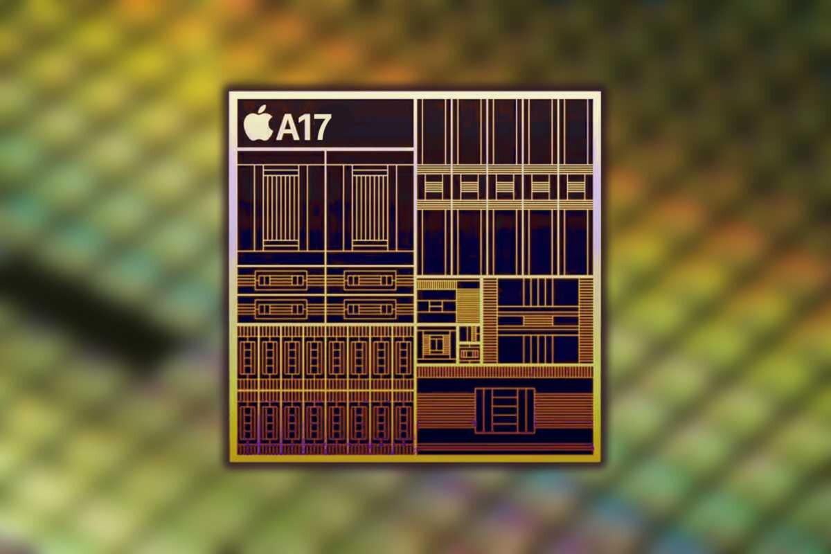
A technology tipster has been dropping multiple tidbits this week about Qualcomm's upcoming Snapdragon 8 Gen 3 mobile chipset - this follows a leak (from a different source, going back to mid-April) about the next generation Adreno 750 GPU getting tuned up for a battle against Apple's Bionic A17 in terms of graphics benchmarks. The latest leak points to the GPU being clocked at 900 MHz, rather than the rumored higher figure of 1.0 GHz speed (garnered from tests at Qualcomm's labs). The focus has now turned to the next generation flagship Snapdragon's CPU aspect, with information emerging about core clock speeds and multiple cluster configurations.

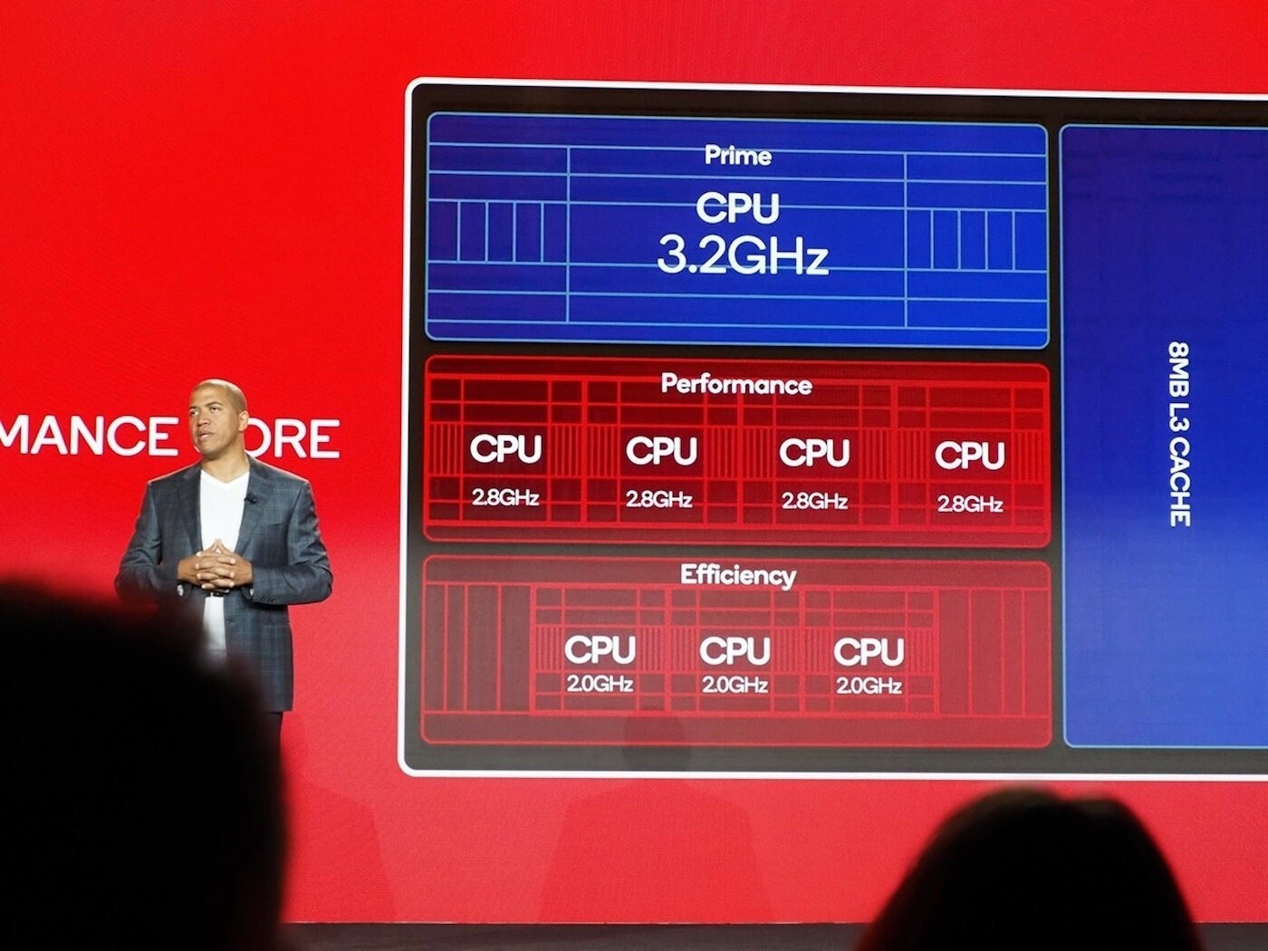
Revegnus suggests that the Snapdragon 8 Gen 3 (SD8G3) chipset will be packing a large primary core in the shape of Arm's Cortex-X4 CPU with a reported maximum clock speed of 3.40 GHz. Leaks from the past have posited that the SD8G3 would feature a fairly standard 1x Large + 5x Big + 2x Small CPU core layout (with clocks predicted to be: large Cortex X4 at 3.2 GHz, big Cortex-A720 at 3.0 GHz, and small Cortex-A520 at 2.0 GHz). An insider source has provided Revegnus with additional information about two different CPU core configurations - 1+5+2 and 2+4+2 - it is theorized that smartphone manufacturers will be offered the latter layout as an exclusive option for special edition flagship phones. The more powerful 2+4+2 variant is said to sacrifice a big core (A720) in favor of a dual Cortex X4 headliner, although the resultant thermal output of twin large cores could prove to be problematic.

Snapdragon 8 Gen 3 GPU Could be 50% More Powerful Than Current Gen Adreno 740

An online tipster, posting on the Chinese blog site Weibo, has let slip that Qualcomm's upcoming Snapdragon 8 Gen 3 mobile chipset is touted to pack some hefty graphical capabilities. The suggested Adreno "750" smartphone and tablet GPU is touted to offer a 50% increase over the present generation Adreno 740 - as featured on the recently released and cutting-edge Snapdragon 8 Gen 2 chipset. The current generation top-of-the-range Snapdragon is no slouch when it comes to graphics benchmarks, where it outperforms Apple's prime contender - the Bionic A16 SoC.

The Snapdragon 8 Gen 3 SoC is expected to launch in the last quarter of 2023, but details of the flagship devices that it will power are non-existent at the time of writing. The tipster suggests that Qualcomm has decided to remain on TSMC's 4 nm process for its next generation mobile chipset - perhaps an all too safe decision when you consider that Apple has upped the stakes with the approach of its Bionic A17 SoC. It has been reported that the Cupertino, California-based company has chosen to fabricate via TSMC's 3 nm process, although the Taiwanese foundry is said to be struggling with its N3 production line. The engineers at Qualcomm's San Diego headquarters are alleged to be experimenting with increased clock speeds running on the next gen Adreno GPU - as high as 1.0 GHz - in order to eke out as much performance as possible, in anticipation of besting the Bionic A17 in graphics benchmarks. The tipster theorizes that Qualcomm will still have a hard time matching Apple in terms of pure CPU throughput, so the consolation prize will lie with a superior GPU getting rigged onto the Snapdragon 8 Gen 3.

AMD Zen 5 "Nirvana" and Zen 6 "Morpheus" Core Codenames Leaked, Confirm Foundry Nodes

An AMD engineer inadvertently leaked the core codenames of the company's upcoming "Zen 5" and "Zen 6" microarchitectures. It's important to understand here what has been leaked. "Zen 5" and "Zen 6" are microarchitecture names, just like the current "Zen 4" and past "Zen 3" or older. AMD uses codenames for the CCD (CPU complex dies) based on these microarchitectures, which it shares between Ryzen client and EPYC enterprise processors. For example, the CCD codename for "Zen 3" is "Brekenridge," and for "Zen 4" it is "Durango." AMD also uses codenames for the CPU cores themselves. "Zen 3" CPU cores are codenamed "Cerebrus," and "Zen 4" CPU cores "Persphone." And now, the leak:

The CCD based on the upcoming "Zen 5" microarchitecture is codenamed "Eldora," and the "Zen 5" CPU core itself is codenamed "Nirvana." There's no codename for the CCD based on "Zen 6," but its CPU cores are codenamed "Morpheus." The "Zen 5" microarchitecture will be based on the 3 nm EUV foundry node; while "Zen 6" will be 2 nm EUV. The engineer in the screenshot is contributing to the power-management technology behind "Zen 5" and "Zen 6," and states that their work on "Zen 5" spanned January-December of 2022, which means the development phase of the next "Zen" architecture is probably complete, and the architecture is undergoing testing and refinement. It's also claimed that work on at least the power-management aspect of "Zen 6" has started from January 2023.

Intel's Next Generation GPUs to be Made by TSMC, Celestial Set for 3 nm Process

Intel has awarded TSMC with some big contracts for future manufacturing of next generation GPUs, according to Taiwan's Commercial Times. As previously covered on TPU, the second generation Battlemage graphics processing units will get fabricated via a 4 nm process. According to insider sources at both partnering companies, Intel is eyeing a release date in the second half of 2024 for this Xe2-based architecture. The same sources pointed to the third generation Celestial graphics processing units being ready in time for a second half of 2026 launch window. Arc Celestial, which is based on the Xe3 architecture, is set for manufacture in the coming years courtesy of TSMC's N3X (3 nm) process node.

One of the sources claim that Intel is quietly confident about its future prospects in the GPU sector, despite mixed critical and commercial reactions to the first generation line-up of Arc Alchemist discrete graphics cards. The company is said to be anticipating great demand for more potent versions of its graphics products in the future, and internal restructuring efforts have not dulled the will of a core team of engineers. The restructuring process resulted in the original AXG graphics division being divided into two sub-groups - CCG and DCAI. The pioneer of the entire endeavor, Raja Koduri, departed Intel midway through last month, to pursue new opportunities with an AI-focused startup.

AMD Speeds Up Development of "Zen 5" to Thwart Intel Xeon "Emerald Rapids"?

In no mood to cede its market-share growth to Intel, AMD has reportedly decided to accelerate the development of its next-generation "Zen 5" microarchitecture for debut within 2023. In its mid-2022 presentations, AMD had publicly given "Zen 5" a 2024 release date. This is part of a reading-in-between the lines for a recent GIGABYTE press release announcing server platforms powered by relatively low-cost Ryzen desktop processors. The specific sentence from that release reads "The next generation of AMD Ryzen desktop processors that will come out later this year will also be supported on this AM5 platform, so customers who purchase these servers today have the opportunity to upgrade to the Ryzen 7000 series successor."

While the GIGABYTE press release speaks of a next-generation Ryzen desktop processor, it stands to reason that it is referencing an early release of "Zen 5," and since AMD shares the CPU complex dies (CCDs) between its Ryzen client and EPYC server processors, the company is looking at a two-pronged upgrade to its processor lineup, with its next-generation EPYC "Turin" processor competing with Xeon Scalable "Emerald Rapids," and Ryzen "Granite Ridge" desktop processors taking on Intel's Core "Raptor Lake Refresh" and "Meteor Lake-S" desktop processors. It is rumored that "Zen 5" is being designed for the TSMC 3 nm node, and could see an increase in CPU core count per CCD, up from the present 8. TSMC 3 nm node goes into commercial mass-production in the first half of 2023 as the TSMC N3 node, with a refined N3E node slated for the second half of the year.

Apple A17 Bionic SoC Performance Targets Could be Lowered

Apple's engineering team is rumored to be adjusting performance targets set for its next generation mobile SoC - the A17 Bionic - due to issues at the TSMC foundry. The cutting edge 3 nm process is proving difficult to handle, according to industry tipsters on Twitter. The leaks point to the A17 Bionic's overall performance goals being lowered by 20%, mainly due to the TSMC N3B node not meeting production targets. The factory is apparently lowering its yield and execution targets due to ongoing problems with FinFET limitations.

The leakers have recently revealed more up-to-date A17 Bionic's Geekbench 6 scores, with single thread performance at 3019, and multi-thread at 7860. Various publications have been hyping the mobile SoC's single thread performance as matching that of desktop CPUs from Intel and AMD, more specifically 13th-gen Core i7 and 'high-end' Ryzen models. Naturally the A17 Bionic cannot compete with these CPUs in terms of multi-thread performance.

TSMC's 3 nm Node at Near 50 Percent Utilisation, Other Nodes Seeing Lower Demand

Based on multiple reports out of Taiwan, TSMC is seeing increased utilisation of its 3 nm node and its production line is now at close to 50 percent utilisation. The main customer here is without a doubt Apple and TSMC is churning out some 50-55,000 wafers a month on its 3 nm node. TSMC is also getting ready to start production on its N3E node later this year, which will see some customers move to the node.

However, it's not all good news, as TSMC is seeing a decline in utilisation on its 5/4 and 7/6 nm nodes as demand has dropped significantly here, with different news outlets reporting different figures. Some are suggesting the 7/6 nm nodes might have dropped as low as to 50 percent utilisation, others mention 70 percent. The 5/4 nm nodes aren't anywhere nearly as badly affected and remain at around 80 percent utilisation. The good news for TSMC is that this is expected to be a temporary slump in demand and most of its leading edge nodes should be back at somewhere around a 90 percent utilisation rate by the second half of the year. However, this depends on what the demand for its partners' products will look like going forward, as many of TSMC's customers are seeing lower demand for their products in turn.

Intel 20A and 18A Foundry Nodes Complete Development Phase, On Track for 2024 Manufacturing

Intel Foundry Services, the in-house semiconductor foundry of Intel, announced that its 2 nm-class Intel 20A and 1.8 nm-class Intel 18A foundry nodes have completed development, and are on course for mass-producing chips on their roadmap dates. Chips are expected to begin mass-production on the Intel 20A node in the first half of 2024, while those on the Intel 18A node are expected to begin in the second half of 2024. The completion of the development phase means that Intel has finalized the specifications and performance/power targets of the nodes, the tools and software required to make the chips, and can now begin ordering them to build the nodes. Intel has been testing these nodes through 2022, and with the specs being finalized, chip-designers can accordingly wrap up development of their products to align with what these nodes have to offer.

Intel 20A (or 20-angstrom, or 2 nm) node introduces gates-all-around (GAA) RibbonFET transistors with PowerVIAs (an interconnect innovation that contributes to transistor densities). The Intel 20A node is claimed to offer a 15% performance/Watt gain over its predecessor, the Intel 3 node (FinFET EUV, 3 nm-class), which by itself offers an 18% performance/Watt gain over Intel 4 (20% perf/Watt gain over the current Intel 7 node), the node that is entering mass-production very soon. The Intel 18A node is a further refinement of Intel 20A, and introduces a design improvement to the RibbonFET that increases transistor density at scale, and a claimed 10% performance/Watt improvement over Intel 20A.

Intel Defers 3 nm Wafer Orders with TSMC, Pushes "Arrow Lake" Rollout to 2025?

Intel has reportedly deferred its orders for 3 nm wafers with TSMC, sources in PC makers tell Taiwan-based industry observer DigiTimes. Built on the TSMC N3 node, the wafers were supposed to power the Graphics tiles (containing the iGPU), of the upcoming "Arrow Lake" processors, which were originally on course for a 2024 release. The DigiTimes report detailing this development says that Intel's 3 nm wafer orders have been deferred to Q4-2024, which would realistically mean a 2025 launch for whatever product was designed to use 3 nm tiles. Advance orders for next-gen wafers by high-volume clients such as Intel, are usually placed several quarters in advance, so the foundry could suitably scale up its capacity.

Samsung Electronics Announces Fourth Quarter and FY 2022 Results, Profits at an 8-year Low

Samsung Electronics today reported financial results for the fourth quarter and the fiscal year 2022. The Company posted KRW 70.46 trillion in consolidated revenue and KRW 4.31 trillion in operating profit in the quarter ended December 31, 2022. For the full year, it reported 302.23 trillion in annual revenue, a record high and KRW 43.38 trillion in operating profit.

The business environment deteriorated significantly in the fourth quarter due to weak demand amid a global economic slowdown. Earnings at the Memory Business decreased sharply as prices fell and customers continued to adjust inventory. The System LSI Business also saw a decline in earnings as sales of key products were weighed down by inventory adjustments in the industry. The Foundry Business posted a new record for quarterly revenue while profit increased year-on-year on the back of advanced node capacity expansion as well as customer base and application area diversification.

Top 10 TSMC Customers Said to have Cut Orders for 2023

On the day of TSMC's celebration of the mass production start of its 3 nm node, news out of Taiwan suggests that all of its top 10 customers have cut their orders for 2023. However, the cuts are unlikely to affect its new node, but rather its existing nodes, with the 7 and 6 nm nodes said to be hit the hardest, by as much as a 50 percent utilisation reduction in the first quarter of 2023. The 28 nm and 5 and 4 nm nodes are also said to be affected, although it's unclear by how much at this point in time.

Revenue is expected to fall by at least 15 percent in the first quarter of 2023 for TSMC, based on numbers from DigiTimes. The fact that TSMC has increased its 2023 pricing by six percent should at least help offset some of the potential losses for the company, but it all depends on the demand for the rest of the year. Demand for mobile devices is down globally, which is part of the reason why so many of TSMC's customers have cut back their orders, as Apple, Qualcomm and Mediatek all produce their mobile SoCs at TSMC. Add to this that the demand for computers and new computer components are also down, largely due to the current pricing and TSMC is in for a tough time next year.

TSMC Holds 3nm Volume Production and Capacity Expansion Ceremony, Marking a Key Milestone for Advanced Manufacturing

TSMC today held a 3 nanometer (3 nm) Volume Production and Capacity Expansion Ceremony at its Fab 18 new construction site in the Southern Taiwan Science Park (STSP), bringing together suppliers, construction partners, central and local government, the Taiwan Semiconductor Industry Association, and members of academia to witness an important milestone in the Company's advanced manufacturing.

TSMC has laid a strong foundation for 3 nm technology and capacity expansion, with Fab 18 located in the STSP serving as the Company's GIGAFAB facility producing 5 nm and 3 nm process technology. Today, TSMC announced that 3 nm technology has successfully entered volume production with good yields, and held a topping ceremony for its Fab 18 Phase 8 facility. TSMC estimates that 3 nm technology will create end products with a market value of US$1.5 trillion within five years of volume production.

TSMC to Mark 3 nm Mass Production Start, Looking at Potential New Fabs in Japan and Germany

According to news out of Taiwan, TSMC will hold a ceremony to mark the official mass production start of its 3 nm node on the 29th of December. This is said to help "shatter doubts about de-Taiwanization" or in simpler terms, that Taiwan will lose its golden goose as TSMC invests abroad. The 3 nm fab—known as fab 18—is based in southern Taiwan's Tainan and the ceremony also marks the start of an expansion of TSMC's most advanced fab. TSMC is said to be kicking off its N3E node production sometime in the second half of 2023, followed by its N3P node in 2024, all of which should take place at fab 18, which also produces 5 nm wafers.

In related news, according to Reuters, a Japanese lawmaker from the ruling party has said that TSMC is considering a second plant in Japan, in addition to its current joint venture that is already under construction. TSMC's response to Reuters was that the company isn't ruling out Japan for future fabs, but that the company doesn't have any current plans. At the same time, TSMC is said to be sending executives to Dresden, Germany in early 2023, for a second round of talks about building a fab to help support the European auto industry, although this would be a 28/22 nm fab, which is far from cutting edge these days, although a lot more advanced than most fabs making chips for the auto industry.

TSMC Announces Updates for TSMC Arizona

TSMC today announced that in addition to TSMC Arizona's first fab, which is scheduled to begin production of N4 process technology in 2024, TSMC has also started the construction of a second fab which is scheduled to begin production of 3 nm process technology in 2026. The overall investment for these two fabs will be approximately US$40 billion, representing the largest foreign direct investment in Arizona history and one of the largest foreign direct investments in the history of the United States.

In addition to the over 10,000 construction workers who helped with construction of the site, TSMC Arizona's two fabs are expected to create an additional 10,000 high-paying high-tech jobs, including 4,500 direct TSMC jobs. When complete, TSMC Arizona's two fabs will manufacture over 600,000 wafers per year, with estimated end-product value of more than US $40 billion.

Alleged Apple M2 Max Performance Figures Show Almost 20% Single-Core Improvement

Apple's ongoing pursuit of leading performance in custom silicon packages continues with each new generation of Apple Silicon. Today, we have alleged Geekbench performance figures of the upcoming M2 Max chip, designed for the upcoming Mac devices. Featuring the same configuration with two E-cores and eight P-cores, the chip is rumored to utilize TSMC's 3 nm design. However, that is yet to be confirmed by Apple, so we don't have the exact information. In the GB5 single-thread test, the CPU set a single-core performance target of 1899 points, while the multi-core score was 8737. While last year's M1 Max chips can reach 1787 single-core and 12826 multi-core scores, these configurations are benchmarked in a Mac Studio, which has better cooling and allows for higher clocks to be achieved.

Apples to apples (pun intended) comparison with the M1 Max chip inside of a MacBook Pro version with presumably the same cooling capacity, which gets 1497 single-core and 11506 multi-core score, the new M2 Max chip is 19.4% faster in single-core results. Multi-core improvements should follow, and this M2 Max result should be different from the final product. We await more benchmarks to confirm this performance increase and the correct semiconductor manufacturing node.

TSMC 3 nm Wafer Pricing to Reach $20,000; Next-Gen CPUs/GPUs to be More Expensive

Semiconductor manufacturing is a significant investment that requires long lead times and constant improvement. According to the latest DigiTimes report, the pricing of a 3 nm wafer is expected to reach $20,000, which is a 25% increase in price over a 5 nm wafer. For 7 nm, TSMC managed to produce it for "just" $10,000; for 5 nm, it costs the company to make it for the $16,000 mark. And finally, the latest and greatest technology will get an even higher price point at $20,000, a new record in wafer pricing. Since TSMC has a proven track record of delivering constant innovation, clients are expected to remain on the latest tech purchasing spree.

Companies like Apple, AMD, and NVIDIA are known for securing orders for the latest semiconductor manufacturing node capacities. With a 25% increase in wafer pricing, we can expect the next-generation hardware to be even more expensive. Chip manufacturing price is a significant price-determining factor for many products, so the 3 nm edition of CPUs, GPUs, etc., will get the highest difference.

TSMC's Morris Chang Says Arizona Fab Will Produce 3 nm Chips in the Future

Although Morris Chang is no longer in charge of the day to day business at TSMC, the founder of the company is still getting his hands dirty. Chang attended the APEC Economic Leaders Meeting last week, as part of Taiwan's delegation and was questioned by the media about TSMC's future plans. The specific question was about TSMC's Arizona fab, which will initially produce chips using a 5 nm node. The US$12 billion plant is scheduled to kick off production at some point in 2024, by which time the 5 nm node should be a commonly used node rather than close to cutting edge.

When questioned about the future of the Arizona fab, Morris Chang answered that it will be moving to a 3 nm node, which is currently TSMC's most cutting edge node, that has gone into volume production earlier this year with th N3 node, which is set to be followed by the N3E node. According to Chang, there's interest by several countries to have TSMC set up fabs there, but apparently this is not something TSMC is considering at the moment. One potential reason for this would be a suitable labour force, something that has already proven to be tough for the Arizona fab.

One of TSMC's Biggest Customers Cuts 3nm Wafer Orders As Consumer Demand Deflates

A major unnamed customer of TSMC has reportedly cut their order for 3 nm wafers. Foundry customers usually place orders for cutting-edge foundry nodes several quarters in advance, in exchange for priority foundry allocations, and preferential rates, while foundries use revenues from these orders to develop the capacity for manufacture these chips. The 3 nm customer could be anyone—Qualcomm, Mediatek, NVIDIA, AMD, or Intel. Order cancellations have reportedly had a domino-effect on the upstream supply-chain of TSMC, hitting suppliers of raw materials, manufacturing equipment, and other consumables. There is an industry-wide slump in demand for consumer electronics and PC hardware, which reflects in the slump in revenues and/or guidance in quarterly financial results releases by prominent companies.

Alphawave IP Achieves Its First Testchip Tapeout for TSMC N3E Process

Alphawave IP (LSE: AWE), a global leader in high-speed connectivity for the world's technology infrastructure, today announced the successful tapeout of its ZeusCORE100 1-112 Gbps NRZ/PAM4 Serialiser-Deserialiser ("SerDes"), Alphawave's first testchip on TSMC's most advanced N3E process. Alphawave IP will be exhibiting this new product alongside its complete portfolio of high-performance IP, chiplet, and custom silicon solutions at the TSMC OIP Forum on October 26 in Santa Clara, CA as the Platinum sponsor.

ZeusCORE100 is Alphawave's most advanced multi-standard-SerDes, supporting extra-long channels over 45dB and the most requested standards such as 800G Ethernet, OIF 112G-CEI, PCIe GEN6, and CXL 3.0. Attendees will be able to visit the Alphawave booth and meet the company's technology experts including members of the recently acquired OpenFive team. OpenFive is a longstanding partner of TSMC through the OIP Value Chain Aggregator (VCA) program. OpenFive is one of a select few companies with an idea-to-silicon methodology in TSMC's latest technologies, and advanced packaging capabilities, enabling access to the most advanced foundry solution available with the best Power-Performance-Area (PPA). With Alphawave's industry-leading IP portfolio and the addition of OpenFive's capabilities, designers can create systems on a chip (SoCs) that pack more compute power into smaller form factors for networking, AI, storage, and high-performance computing (HPC) applications.

Samsung Electronics Unveils Plans for 1.4 nm Process Technology

Samsung Electronics, a world leader in advanced semiconductor technology, announced today a strengthened business strategy for its Foundry Business with the introduction of cutting-edge technologies at its annual Samsung Foundry Forum event. With significant market growth in high-performance computing (HPC), artificial intelligence (AI), 5/6G connectivity and automotive applications, demand for advanced semiconductors has increased dramatically, making innovation in semiconductor process technology critical to the business success of foundry customers. To that end, Samsung highlighted its commitment to bringing its most advanced process technology, 1.4-nanometer (nm), for mass production in 2027.

During the event, Samsung also outlined steps its Foundry Business is taking in order to meet customers' needs, including: foundry process technology innovation, process technology optimization for each specific applications, stable production capabilities, and customized services for customers. "The technology development goal down to 1.4 nm and foundry platforms specialized for each application, together with stable supply through consistent investment are all part of Samsung's strategies to secure customers' trust and support their success," said Dr. Si-young Choi, president and head of Foundry Business at Samsung Electronics. "Realizing every customer's innovations with our partners has been at the core of our foundry service."

AMD's CEO Lisa Su Planning Trip to Taiwan, Said to be Visiting TSMC to Secure Future Wafer Allocation

Based on a report by Tom's Hardware, AMD's CEO Lisa Su is planning a trip to Taiwan in the next couple of months. It is said that she is planning to meet with multiple partners in Taiwan, such as ASUS, Acer and maybe more importantly, ASMedia, which will be the sole maker of chipsets for AMD, once the X570 chipset is discontinued. AMD is apparently also seeing various less well known partners that deliver parts for its CPUs, such as Nan Ya PCB, Unimicron Technologies and Kinsus Interconnects.

However, it appears that the main reason for Lisa Su herself to visit Taiwan will be to meet with TSMC, to discuss future collaboration with CC Wei, TSMC's chief executive. This is so AMD can secure enough wafer allocation on future nodes, such as its 3 nm and 2 nm class nodes. The move to these nodes is obviously not happening in the near future for AMD, but considering that TSMC is currently the leading foundry and is operating at capacity, it makes sense to get in early, as the competition is stiff when it comes to getting wafer allocation on cutting edge nodes. It's unclear which exact 3 nm class node AMD will be aiming for, but it might be the N3P node, which is said to kick off production sometime next year. Lisa Su is also said to have meetings with TSMC, SPIL and Ase Technology when it comes to advanced packaging for AMD's products. This includes technologies such as chip-on-wafer-on-substrate (CoWoS) and fan-out embedded bridge (FO-EB), with AMD already being expected to use some of these technologies in its upcoming Navi 3x GPUs.

AMD Confirms Optical-Shrink of Zen 4 to the 4nm Node in its Latest Roadmap

AMD in its Ryzen 7000 series launch event shared its near-future CPU architecture roadmap, in which it confirmed that the "Zen 4" microarchitecture, currently on the 5 nm foundry node, will see an optical-shrink to the 4 nm process in the near future. This doesn't necessarily indicate a new-generation CCD (CPU complex die) on 4 nm, it could even be a monolithic mobile SoC on 4 nm, or perhaps even "Zen 4c" (high core-count, low clock-speed, for cloud-compute); but it doesn't rule out the possibility of a 4 nm CCD that the company can use across both its enterprise and client processors.

The last time AMD hyphenated two foundry nodes for a single generation of the "Zen" architecture, was with the original (first-generation) "Zen," which debuted on the 14 nm node, but was optically shrunk and refined on the 12 nm node, with the company designating the evolution as "Zen+." The Ryzen 7000-series desktop processors, as well as the upcoming EPYC "Genoa" server processors, will ship with 5 nm CCDs, with AMD ticking it off in its roadmap. Chronologically placed next to it are "Zen 4" with 3D Vertical Cache (3DV Cache), and the "Zen 4c." The company is planning "Zen 4" with 3DV Cache both for its server- and desktop segments. Further down the roadmap, as we approach 2024, we see the company debut the future "Zen 5" architecture on the same 4 nm node, evolving into 3 nm on certain variants.

TSMC has Seven Major Customers Lined Up for its 3 nm Node

Based on media reports out of Taiwan, TSMC seems to have plenty of customers lined up for its 3 nm node, with Apple being the first customer out the gates when production starts sometime next month. However, TSMC is only expected to start the production with a mere 1,000 wafer starts a month, which seems like a very low figure, especially as this is said to remain unchanged through all of Q4. On the plus side, yields are expected to be better than the initial 5 nm node yields. Full-on mass production for the 3 nm node isn't expected to happen until the second half of 2023 and TSMC will also kick off its N3E node sometime in 2023.

Apart from Apple, major customers for the 3 nm node include AMD, Broadcom, Intel, MediaTek, NVIDIA and Qualcomm. Contrary to earlier reports by TrendForce, it appears that TSMC will continue its rollout of the 3 nm node as previously planned. Apple is expected to produce the A17 smartphone and tablet SoC, as well as advanced versions of the M2, as well as the M3 laptop and desktop processors on the 3 nm node. Intel is still said to be producing its graphics chiplets with TSMC, with the potential for GPU and FPGA products in the future. There's no word on what the other customers are planning to produce on the 3 nm node, but MediaTek and Qualcomm are obviously looking at using the node for future smartphone and tablet SoCs, with AMD and NVIDIA most likely aiming for upcoming GPUs and Broadcom for some kind of HPC related hardware.

Intel Meteor Lake Reportedly Delayed Until End of 2023, Will Have Knock-On Effects for TSMC

Based on a report by TrendForce, Intel has yet again had to push back its upcoming Meteor Lake CPUs and it now appears that Intel will only be launching Meteor Lake towards the end of 2023. It's unclear why there has been yet another delay, but Intel is said to have cancelled most of its orders with TSMC for the 3 nm tGPU that Intel will have made at TSMC, for 2023. The knock-on effect of this, is that TSMC is said to be slowing down its production line expansion towards 3 nm, as the company is now unsure if it'll be able to fill its order books for all of 2023. TSMC's main customer for the 3 nm node is still going to be Apple, but with the loss of what is likely to be around six months worth of production from Intel, TSMC is said to be considering cutting its CapEx for 2023.

TSMC's other customers, such as AMD, MediaTek and Qualcomm aren't planning on moving to 3 nm until 2024, so unless there's a change in plans from either of these companies, or increased demand from Apple, TSMC is said to hit the brakes when it comes to starting up new, cutting edge production lines next year. TSMC is also likely to see reduced revenues during 2023 due to Intel's change of plans, although it's too early to make any assumptions. TrendForce also suggests that Intel might still use TSMC's 3 nm node as a backup plan, if Intel would fail to execute on moving to the Intel 4 process, but considering how complex it is to move a design between different foundry processes, this seems unlikely.

Samsung Begins Chip Production Using 3nm Process Technology With GAA Architecture

Samsung Electronics, the world leader in semiconductor technology, today announced that it has started initial production of its 3-nanometer (nm) process node applying Gate-All-Around (GAA) transistor architecture. Multi-Bridge-Channel FET (MBCFET), Samsung's GAA technology implemented for the first time ever, defies the performance limitations of FinFET, improving power efficiency by reducing the supply voltage level, while also enhancing performance by increasing drive current capability. Samsung is starting the first application of the nanosheet transistor with semiconductor chips for high performance, low power computing application and plans to expand to mobile processors.

"Samsung has grown rapidly as we continue to demonstrate leadership in applying next-generation technologies to manufacturing, such as foundry industry's first High-K Metal Gate, FinFET, as well as EUV. We seek to continue this leadership with the world's first 3 nm process with the MBCFET," said Dr. Siyoung Choi, President and Head of Foundry Business at Samsung Electronics. "We will continue active innovation in competitive technology development and build processes that help expedite achieving maturity of technology."
Return to Keyword Browsing
May 21st, 2024 21:36 EDT change timezone

New Forum Posts

Popular Reviews

Controversial News Posts