News Posts matching #3 nm

Return to Keyword Browsing

TSMC Announces the N3 FinFlex, N3E, and N2 Nodes, and 3DFabric

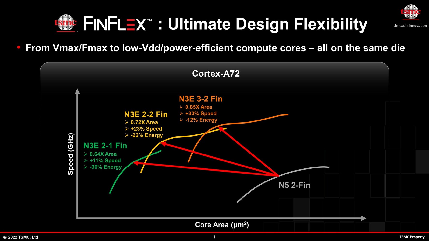
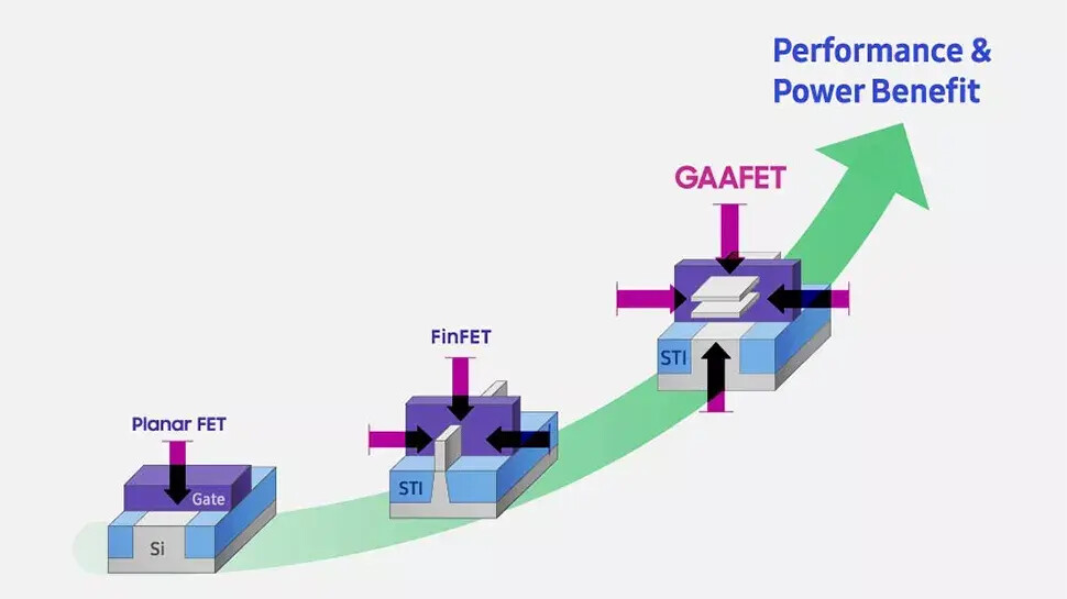
TSMC today showcased the newest innovations in its advanced logic, specialty, and 3D IC technologies at the Company's 2022 North America Technology Symposium, with the next-generation leading-edge N2 process powered by nanosheet transistors and the unique FINFLEX technology for the N3 and N3E processes making their debut.

Resuming as an in-person event after being held online in the past two years, the North America symposium in Santa Clara, California, kicks off a series of Technology Symposiums around the world in the coming months. The Symposiums also feature an Innovation Zone that spotlights the achievements of TSMC's emerging start-up customers.

Intel "Meteor Lake-P" SoC with 6P+8E Compute Tile Pictured

Intel's next-generation "Meteor Lake-P" mobile processor with a 6P+8E Compute Tile was shown off at the 2022 IEEE VLSI Symposium on Tech and Circuits (6 performance cores and 8 efficiency cores). We now have annotations for all four tiles, as well as a close-up die-shot of the Compute Tile. Intel also confirmed that the Compute Tile will be built on its homebrew Intel 4 silicon fabrication process, which offers over 20% iso-power performance increase versus the Intel 7 node, through extensive use of EUV lithography.

We had earlier seen a 2P+8E version of the "Meteor Lake" Compute Tile, probably from the "Meteor Lake-U" package. The larger 6P+8E Compute tile features six "Redwood Cove" performance cores, and two "Crestmont" efficiency core clusters, each with four E-cores. Assuming the L3 cache slice per P-core or E-core cluster is 2.5 MB, there has to be 20 MB of L3 cache on the compute tile. Each P-core has 2 MB of dedicated L2 cache, while each of the two E-core clusters shares 4 MB of L2 cache among four E-cores.

Samsung Foundry Considering up to 20 Percent Price Hikes

Earlier this week, news about TSMC increasing prices in 2023 made its way online and now Samsung Foundry is said to be discussing price hikes with its customers to make up for the increased costs in materials. TSMC already increased its prices by around 20 percent at the end of 2021 and now it looks like Samsung Foundry is set to follow suit with a similar price hike. Depending on the node, the company is said to be looking at increases of between 15 to 20 percent. The somewhat peculiar thing in the case of Samsung Foundry, is that the company is looking at asking for more money on older, legacy nodes, than it will for its cutting edge nodes.

The price increases are said to come into effect sometime in the second half of 2022, so more than six months after TSMC's price hike. The company is still in negotiation with some of its customers, while others have already come to an agreement with Samsung Foundries. The costs to produce chips are said to be increasing by 20 to 30 percent across the board, no matter if we're talking materials needed to produce integrated circuits, or building new factories, according to Bloomberg. Samsung Foundries have also managed to secure long-term orders for the next five years, with a combined value of around eight times that of previous year's revenue, according to its EVP, Kang Moon-soo. The company is hoping to overtake TSMC in the future and invested more than US$36 billion in 2021 alone to expand its foundry business with new fabs and EUV machines. The good news is that Samsung Foundry claims to be back on track when it comes to yield on its 4 nm node and mass production of its 3 nm node is said to start this quarter.

Samsung Says Future Fab Nodes Are On Time, no Yield Issues on Current Nodes

Despite rumours of both production issues and node delays, Samsung has assured its shareholders during its first quarter conference call, that the company is on track. Its yield rate from its 5 nm node was said to have entered maturity, meaning that yields have entered Samsung's expected levels. However, Samsung did admit that its 4 nm node had seen some delays with the ramp up, but it has now entered the expected yield rate curve. The company is also working on an new R&D line for its upcoming 3 nm node, but didn't go into any further details.

As for Samsung's DRAM products, there were rumours that its 12 nm 1b process node had hit some snags and that the company was going to skip ahead to its 1c node, something the company denied. Samsung added that the development of 1b was proceeding stably and that the 1c node is expected to be done on schedule. The company also said that media reports of issues at Samsung's foundry business were overblown and that order books are full, which is why some of its customers have had to produce additional parts with TSMC. Samsung's foundry business reportedly saw an increase in operating profit of 50 percent compared to last year, as well as an increase in revenue of 19 percent.

TSMC's N3E Node Said to Have Good Yields, Volume Production Expected Q2 2023

Back in March there were reports of TSMC's N3E node having been moved from 2024 to the end of 2023. However, it seems like the node is already seeing better than expected yields and is now being pulled in further and TSMC is expecting to start volume production as early as Q2 in 2023. The node does appear to have been frozen when it comes to further development as of the end of March. Yields are said to be much higher than the N3B node, which is also under development, but with limited information available about it.

The first customer for the new node is expected to be Apple, as the company is largely paying for much of the cutting edge node development at TSMC. However, both Intel and Qualcomm are said to be some of the first customers for the new node. More details should hopefully be announced tomorrow during TSMC's first quarter earnings call. The N3E node is a reduced layer EUV process, but before it goes into mass production, it's likely we'll be seeing the N3 node first. Early production of 3 nm parts later this year is expected to be at around 10 to 20k wafers per month initially, rising to about 25 to 35k a month once TSMC's new fab is ready. Once the N3E node is in full swing, the monthly capacity of 3 nm parts should be around 50k wafers a month, but depending on customer demand, it might end up being even higher.

Samsung Foundry Looks to Legacy Nodes for Expansion

While there's a lot of talk about cutting edge nodes, Samsung Foundries are looking at alternative options to find new business and are said to be eyeing legacy nodes for future expansions. At the same time, Samsung is looking at setting up its own chip testing and packaging factory, to be able to better serve customers who are looking for a full-service partner. It's not clear which legacy nodes Samsung are eyeing, but the story by Business Korea states that at least some of it will focus on CMOS imaging sensors, since there is apparently a shortage of those too.

Samsung is said to have plans for no less than 300 new customers by 2026 for its foundry business, across all nodes. However, this doesn't mean Samsung will stop developing new, cutting edge nodes, as Samsung is still planning to kick off volume production on its 3 nm node in the first half of this year, with 2 nm said to start volume production in 2025. After its dealings with Nvidia and Qualcomm that haven't been what you'd call successful, the question is who will be willing to partner with Samsung Foundry on its cutting edge nodes in the future.

Qualcomm Said to be Moving to TSMC for 3 nm Chips

Although nothing has been officially confirmed by Qualcomm, it looks like the company will be moving away from Samsung for its 3 nm based chips, in favour of TSMC. The Elec also mentions that Qualcomm has moved some of its Snapdragon 8 Gen 1 production to TSMC, something that has already been hitting the rumour mill. The first batch of 4 nm Snapdragon 8 Gen 1 chips are said to already have entered the early stages of production. The main reason for the move is said to be poor yields by Samsung Foundry on its 4 nm node.

The yield rates are said to be a measly 35 percent for the Snapdragon 8 Gen 1, with Samsung's Exynos 2200 having even lower yields. This also helps explain why Samsung's mobile division has decided to limit the availability of its Exynos 2200 based phones to only a few regions. Apparently Qualcomm had to send staff over to Korea to help get the yields up to their current rate, but it's not hard to see why the company is shifting back to TSMC, as a 35 percent yield rate is simply not acceptable. Samsung is said to be auditing Samsung Foundry to find out what has gone wrong, as anything below 80-90 percent in terms of yield rate is simply not acceptable for mass production. Qualcomm will apparently continue to use Samsung Foundry for its 7 nm RF chips, where the yields must be within industry norms.

Samsung Employees Being Investigated for "Fabricating" Yields

Samsung Electronics is hit by a major scandal involving current and former employees. It's being alleged that these employees are involved in falsifying information about the semiconductor fabrication yields of the company's 3/4/5 nanometer nodes to clear them for commercial activity. This came to light when Samsung was observing lower than expected yields after the nodes were approved for mass-production of logic chips for Samsung, as well as third-party chip-designers. A falsified yield figure can have a cascading impact across the supply-chain, as wafer orders and pricing are decided on the basis of yields. Samsung however, has downplayed the severity of the matter. The group has initiated an investigation into Samsung Device Solutions, the business responsible for the foundry arm of the company. This includes a thorough financial audit of the foundry to investigate if the investments made to improve yields were properly used.

Intel "Meteor Lake" and "Arrow Lake" Use GPU Chiplets

Intel's upcoming "Meteor Lake" and "Arrow Lake" client mobile processors introduce an interesting twist to the chiplet concept. Earlier represented in vague-looking IP blocks, new artistic impressions of the chip put out by Intel shed light on a 3-die approach not unlike the Ryzen "Vermeer" MCM that has up to two CPU core dies (CCDs) talking to a cIOD (client IO die), which handles all the SoC connectivity; Intel's design has one major difference, and that's integrated graphics. Apparently, Intel's MCM uses a GPU die sitting next to the CPU core die, and the I/O (SoC) die. Intel likes to call its chiplets "tiles," and so we'll go with that.

The Graphics tile, CPU tile, and the SoC or I/O tile, are built on three different silicon fabrication process nodes based on the degree of need for the newer process node. The nodes used are Intel 4 (optically 7 nm EUV, but with characteristics of a 5 nm-class node); Intel 20A (characteristics of 2 nm), and external TSMC N3 (3 nm) node. At this point we don't know which tile gets what. From the looks of it, the CPU tile has a hybrid CPU core architecture made up of "Redwood Cove" P-cores, and "Crestmont" E-core clusters.

Tachyum Selected for Pan-European Project Enabling 1 AI Zettaflop in 2024

Tachyum today announced that it was selected by the Slovak Republic to participate in the latest submission for the Important Projects of Common European Interest (IPCEI), to develop Prodigy 2 for HPC/AI. Prodigy 2 for HPC/AI will enable 1 AI Zettaflop and more than 10 DP Exaflops computers to support superhuman brain-scale computing by 2024 for under €1B. As part of this selection, Tachyum could receive a 49 million Euro grant to accelerate a second-generation of its Tachyum Prodigy processor for HPC/AI in a 3-nanometer process.

The IPCEI program can make a very important contribution to sustainable economic growth, jobs, competitiveness and resilience for industry and the economy in the European Union. IPCEI will strengthen the EU's open strategic autonomy by enabling breakthrough innovation and infrastructure projects through cross-border cooperation and with positive spill-over effects on the internal market and society as a whole.

Intel and TSMC Strike 3nm Deal, New Hsinchu Fab to Cater to Intel

It looks like Intel and TSMC have a deal in place to manufacture 3 nm chips. The world-leading Taiwanese fab is setting up a new facility exclusively to cater to Intel, according to DigiTimes, citing industry sources. This facility will be located in the Baoshan area of Hsinchu, in northern Taiwan. The 3 nm node will enable Intel to keep its newfound cadence of launching new CPU microarchitectures with IPC increases each year. The annual IPC increase cadence in particular, would be faster than even the "Tick-Tock" cadence prior to 2015, as the company pushed IPC increases and foundry nodes each alternating year. The company faces stiff competition from AMD, which has been posting IPC increases each year since 2017, and leveraged TSMC 7 nm nodes to beat Intel in the IPC game for the first time in over 17 years.

AMD to Tap Samsung's 4 nm Process for Chromebook Processors, Notes the Report from J.P. Morgan

Historically, AMD was working with two semiconductor manufacturing companies: TSMC and GlobalFoundries. According to the latest report coming from Gokul Hariharan, an analyst at J.P. Morgan, AMD could soon tap another semiconductor manufacturer to produce the company's growing list of processors. As the report indicates, AMD could start working with the South Korean giant Samsung and utilize the firm's 4LPP process that represents a second generation of the low-power 4 nm silicon node. This specific node is allegedly the choice for AMD APUs designed to fit inside Google's Chromebook devices, which require low-power designs to achieve excellent battery life.

AMD could realize this move in late 2022, as Samsung's 4LPP node goes into mass production at that point. It means that we could see the first Samsung-made AMD APUs in late 2022 or the beginning of 2023. And apparently, the two company's collaboration could be much more significant as AMD is evaluating Samsung's 3 nm nodes for other products spanning more segments in 2023/2024. There are no official, definitive agreements between the two, so we have to wait for more information and official responses from these parties. Anyways, if AMD decides to produce a part of its lineup at Samsung, the remaining TSMC capacity would ensure that the supply of every incoming chip remains sufficient.

Intel Negotiates 3nm Allocation with TSMC Even as Pat Gelsinger Cautions Against Investing in Taiwan

Intel is reportedly in talks with TSMC to secure foundry allocation to meet its product roadmap execution. The company is sending an executive delegation to meet with TSMC later this month, to secure foundry capacity for the N3 (3 nm) silicon fabrication node, and ensure that Intel's allocation isn't affected by other customers such as Apple. As part of its IDM 2.0 strategy, Intel has decided to build its products essentially as multi-chip modules with each block of IP built on a silicon fabrication node most optimal to it, so the company maximizes cutting-edge foundry nodes only on the technology that benefits from it the most. N3 will play a vital role with logic/compute tiles in products bound for 2023, as N3 hits critical volume in the first half of the year.

In related news, Intel CEO Pat Gelsinger speaking at the Fortune Brainstorm Tech conference, stressed on the importance for American chip designers to seek out semiconductor manufacturing in America, and cautioned against investing in Taiwan (without naming TSMC). This comes in the wake of geopolitical uncertainty in the region. In response to this statement issued to DigiTimes, TSMC CEO Mark Liu downplayed the matter, and said that Gelsinger's statement wasn't worth responding to, and that he doesn't slander industry colleagues. TSMC and Samsung have each announced multi-billion Dollar foundry investments in the US, in attempts to make the global semiconductor supply chains resilient to any security situation that may emerge in East Asia.

Intel "Meteor Lake" Chips Already Being Built at the Arizona Fab

With its 12th Gen Core "Alder Lake-P" mobile processors still on the horizon, Intel is already building test batches of the 14th Gen "Meteor Lake" mobile processors, at its Fab 42 facility in Chandler, Arizona. "Meteor Lake" is a multi-chip module that leverages Intel's Foveros packaging technology to combine "tiles" (purpose built dies) based on different silicon fabrication processes depending on their function and transistor-density/power requirements. It combines four distinct tiles across a single package—the compute tile, with the CPU cores; the graphics tile with the iGPU: the SoC I/O tile, which handles the processor's platform I/O; and a fourth tile, which is currently unknown. This could be a memory stack with similar functions as the HBM stacks on "Sapphire Rapids," or something entirely different.

The compute tile contains the processor's various CPU core types. The P cores are "Redwood Cove," which are two generations ahead of the current "Golden Cove." If Intel's 12-20% generational IPC uplift cadence holds, we're looking at cores with up to 30% higher IPC than "Golden Cove" (50-60% higher than "Skylake."). "Meteor Lake" also debuts Intel's next-generation E-core, codenamed "Crestmont." The compute tile is rumored to be fabricated on the Intel 4 node (optically a 7 nm-class node, but with characteristics similar to TSMC N5).

TSMC 3 nm To Enter Volume Production in 2022

TSMC will commercialize its N3 (3 nm) EUV silicon fabrication node in 2022, with volume production set to commence in the second half of the year. The company is looking to maximize capacity on its current N5 (5 nm) node, which already serves major customers such as Apple. AMD is expected to utilize N5 allocation going into 2022 as its next-generation "Zen 4" processors are expected to leverage the node to drive up CPU core counts and caches. The company is also utilizing N6 (6 nm) for its CDNA2 compute accelerator logic dies. N5 could also power mobile application processors from several manufacturers.

Samsung Foundry Announces GAA Ready, 3nm in 2022, 2nm in 2025, Other Speciality Nodes

Samsung Electronics, a world leader in advanced semiconductor technology, today unveiled plans for continuous process technology migration to 3- and 2-nanometer (nm) based on the company's Gate-All-Around (GAA) transistor structure at its 5th annual Samsung Foundry Forum (SFF) 2021. With a theme of "Adding One More Dimension," the multi-day virtual event is expected to draw over 2,000 global customers and partners. At this year's event, Samsung will share its vision to bolster its leadership in the rapidly evolving foundry market by taking each respective part of foundry business to the next level: process technology, manufacturing operations, and foundry services.

"We will increase our overall production capacity and lead the most advanced technologies while taking silicon scaling a step further and continuing technological innovation by application," said Dr. Siyoung Choi, President and Head of Foundry Business at Samsung Electronics. "Amid further digitalization prompted by the COVID-19 pandemic, our customers and partners will discover the limitless potential of silicon implementation for delivering the right technology at the right time."

Fabricating the Fabs: ASML Vision Document Predicts 300 Billion-Transistor Logic by 2030

"Moore's Law is alive and well," says ASML, in its vision document addressing investors. The company manufactures the machines that perform the actual task of silicon lithography—turning silicon discs into wafers of logic or storage chips. It highlighted the various technologies making progress, which will help its semiconductor-fabrication customers, such as TSMC and their hundreds of clients, sustain Moore's Law all the way through this decade. The company predicts SoCs with as many as 300 billion transistors by 2030. To achieve this, the company is innovating in two distinct directions—at the chip-level, to increase transistor density per chip to over 50 billion transistors; and at the system level, through packaging technology innovations, to reach that ultimate transistor count.

According to ASML's roadmap, at the turn of the decade, its technology enables 5 nm-class in production, and is at the cusp of a major breakthrough, nanosheet-FETs. which pave the way for 3 nm and 2 nm nodes, backed by EUV lithography. The journey from 2 nm to 1.5 nm will require another breakthrough, forked-nanosheets, and from 1.5 nm to 1 nm yet another breakthrough, CFET. Sub-1 nm fabrication will be possible toward the turn of this decade, thanks to 2D atomic channel technology, which is how chip-designers will be able to cram over 50 billion transistors per chip, and build MCM systems with over 300 billion transistors. The presentation predicts that besides 3D packaging, stacked silicon will also play a role, with multiple stacked logic layers, heterogenous chips with logic, storage, and I/O layers, stacked DRAM (up from single-digit layers to double-digits; and for NAND flash to grow from the current 176-layer, to nearly 500-layer by 2030.

Applied Materials Breakthrough in Chip Wiring Enables Logic Scaling to 3nm and Beyond

Applied Materials, Inc. today unveiled a new way to engineer the wiring of advanced logic chips that enables scaling to the 3 nm node and beyond. While size reduction benefits transistor performance, the opposite is true in the interconnect wiring: smaller wires have greater electrical resistance which reduces performance and increases power consumption. Without a materials engineering breakthrough, interconnect via resistance would increase by a factor of 10 from the 7 nm node to the 3 nm node, negating the benefits of transistor scaling.

Applied Materials has developed a new materials engineering solution called the Endura Copper Barrier Seed IMS. It is an Integrated Materials Solution that combines seven different process technologies in one system under high vacuum: ALD, PVD, CVD, copper reflow, surface treatment, interface engineering and metrology. The combination replaces conformal ALD with selective ALD, eliminating a high-resistivity barrier at the via interface. The solution also includes copper reflow technology that enables void free gap fill in narrow features. Electrical resistance at the via contact interface is reduced by up to 50 percent, improving chip performance and power consumption, and enabling logic scaling to continue to 3 nm and beyond.

AMD Ryzen 8000 Series Processors Based on Zen 5 Architecture Reportedly Codenamed "Granite Ridge"

Today, we have talked about AMD's upcoming Raphael lineup of processors in the article you can find here. However, it seems like the number of leaks on AMD's plans just keeps getting greater. Thanks to the "itacg" on Weibo, we have learned that AMD's Ryzen 8000 desktop series of processors are reportedly codenamed as Granite Ridge. This new codename denotes the Zen 5 based processors, manufactured on TSMC's 3 nm (N3) node. Another piece of information is that AMD's Ryzen 8000 series APUs are allegedly called Strix Point, and they also use the 3 nm technology, along with a combination of Zen 5 and Zen 4 core design IPs. We are not sure how this exactly works out, so we have to wait to find out more.

Samsung Demonstrates 256 Gb 3 nm MBCFET Chip at ISSCC 2021

During the IEEE International Solid-State Circuits Conference (ISSCC), Samsung Foundry has presented a new step towards smaller and more efficient nodes. The new chip that was presented is a 256 Gb memory chip, based on SRAM technology. However, all of that doesn't sound interesting, until we mention the technology that is behind it. Samsung has for the first time manufactured a chip using the company's gate-all-around field-effect transistor (GAAFET) technology on the 3 nm semiconductor node. Formally, there are two types of GAAFET technology: the regular GAAFET that uses nanowires as fins of the transistor, and MBCFET (multi-bridge channel FET) that uses thicker fins that come in a form of a nanosheet.

Samsung has demonstrated the first SRAM chip that uses MBCFET technology today. The chip in question is a 256 Gb chip with an area of 56 mm². The achievement Samsung is proud of is that the chip uses 230 mV less power for writes, compared to the standard approach, as the MBCFET transistors allow the company to have many different power-saving techniques. The new 3 nm MBCFET process is expected to get into high-volume production sometime in 2022, however, we are yet to see demos of logic chips besides SRAM like we see today. Nonetheless, even the demonstration of SRAM is big progress, and we are eager to see what the company manages to build with the new technology.

TSMC Could Build Six GigaFabs in Arizona

Taiwan Semiconductor Manufacturing Company (TSMC), one of the largest manufacturers of silicon, is seemingly making plans to build as many as six of its US-based fabs in Arizona. According to the unconfirmed report coming from UDN, TSMC could be building its Arizona-based factories for much larger capacities. Based on TSMC's classifications, the MegaFab-class of factories is the one with 25,000 WSPM output. According to the report, TSMC plans to build six additional facilities in the area where the Arizona fab is, and have a GigaFab-class (even larger type) factory present on US soil. Currently, the company operates six GigaFabs and all of them are based in Taiwan.

The GigaFab class factory is supposed to have over 100,000 WSPM output, and by building one in the US, TSMC could get much closer to big customers like Apple, NVIDIA, and AMD. Reports are saying that TSMC's primary target is 3 nm node production on 12-inch (300 mm) wafers. All six of the supposed facilities are expected to output more than 100,000 wafers at their peak, making it one of the largest projects TSMC has ever done. The Arizona location is supposed to serve as a "mega fab" facility and it is supposed to start manufacturing silicon in 2024. This information is, of course, just a rumor so you should take it with a grain of salt, as this type of information is usually only known by top-level management.

TSMC to Start 3 nm Node Production This Year

Taiwan Semiconductor Manufacturing Company (TSMC), the leading provider of semiconductors, is supposed to start 3 nm node production this year. While Samsung, one of the top three leading semiconductor foundries, has been struggling with the pandemic and delayed its 3 nm node for 2022, TSMC has managed to deliver it this year. According to a report, the Taiwanese semiconductor giant is preparing the 3 nm node for the second half of this year, with the correct date of high-volume product unknown. The expected wafer capacity for the new node is supposed to be around 30,000 wafers per month, with capacity expansion expected to hit around 105,000 wafers per month in 2023. This is similar to 5 nm's current numbers of 105,000 wafers per month output, which was 90,000 just a few months ago in Q4 2020. One of the biggest customers of the upcoming 3 nm node is Apple.

Samsung to Build $17 Billion Silicon Manufacturing Plant in the US by 2023

Samsung has been one of the world's biggest foundries and one of three big players still left in the leading-edge semiconductor process development and manufacturing. However, the Korean giant is always seeking ways to improve its offerings, especially for Western customers. Today, it is reported that Samsung has reportedly talked with regulators in Texas, New York, and Arizona about building a $17 billion silicon manufacturing facility in the United States. The supposed factory is going to be located near Austin, Texas, and is supposed to offer around 1800 jobs. If the deal is approved and Samsung manages to complete the project on time, the factory is supposed to start mass production in Q4 of 2023.

What process is Samsung going to manufacture in the new fab? Well, current speculations are pointing out to the 3 nm node, with Samsung's special GAAFET (Gate All Around FET) technology tied to the new node. The fab is also expected to make use of extreme ultraviolet (EUV) lithography for manufacturing. Samsung already has a facility in the US called S2, however, that will not be upgraded as it is still serving a lot of clients. Instead, the company will build new facilities to accommodate the demand for newer nodes. It is important to note that Samsung will not do any R&D work in the new fab, and the company will only manufacture the silicon there.

Intel Reportedly Signs Deal with TSMC To Outsource 3 nm Production

We recently reported on Intel's goal to launch their 7 nm node in 2023 which would put them on track to directly compete with TSMC's 3 nm node. It would seem like Intel has partially accepted defeat according to a recent DigiTimes report which alleges that Intel has signed a deal with TSMC to mass-produce 3 nm processors starting H2 2022. The report goes on to detail an arrangement where TSMC manufacturers the bulk of Intel processors with in-house production expected to continue albeit at lower quantities. This arrangement would also see Intel and TSMC cooperate on 2 nm products. If this deal turns out to be real Intel would become TSMC's second-largest customer after Apple.

TSMC to Put Away More Capacity for Automotive Industry if Possible

TSMC is one of the world's biggest semiconductor manufacturers, and the company is currently the leading provider of the newest technologies like 5 nm and 3 nm, along with advanced packaging. So far, TSMC's biggest customers have included Apple, NVIDIA, AMD, etc., where the company has mainly produced chips for mobile phones and PCs/Servers. However, Taiwan's Economics Ministry has announced that they have spoken to TSMC and have reached an agreement that the company will be putting away some additional capacity for the automotive industry, specifically for the production of automotive chips. The reason for this push is the increasing shortage of semiconductors for automakers, experienced due to the Trump administration sanctions against key Chinese chip factories.

TSMC has stated that "Other than continuously maximizing utilization of our existing capacity, Dr. Wei also confirmed in our investors' conference that we are working with customers closely and moving some of their mature nodes to more advanced nodes, where we have a better capacity to support them". The company also states that their capacities are fully utilized for now, however, TSMC has ensured ministry that "if production can be increased by optimizing production capacity, it will cooperate with the government to regard automotive chips as a primary application." That means that TSMC will not decrease any existing capacity, but rather just evaluate any increased capacity for automotive chip production.
Return to Keyword Browsing
May 21st, 2024 16:31 EDT change timezone

New Forum Posts

Popular Reviews

Controversial News Posts