News Posts matching #3 nm

Return to Keyword Browsing

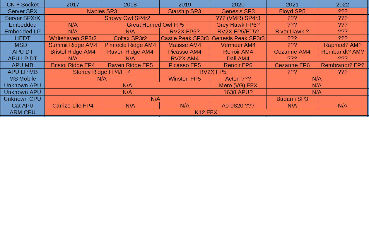
Intel Has Fixed its 7 nm Node, But Outsourcing is Still Going to Happen

Intel has today reported its Q4 2020 earnings disclosing full-year revenue with the current CEO Bob Swan, upcoming new CEO Pat Gelsinger, and Omar Ishrak, Chairman of Intel's board. During the call, company officials have talked about Intel's earnings and most importantly, addressing the current problems about the company's manufacturing part - semiconductor foundries. Incoming Intel CEO, Pat Gelsinger, has talked about the state of the 7 nm node, giving shareholders reassurance and a will to remain in such a position. He has made an argument that he has personally reviewed the progress of the "health and recovery of the 7 nm program."

The 7 nm node has been originally delayed by a full year amid the expectations, and as with the 10 nm node, we have believed that it is going to experience similar issues. However, the incoming CEO has reassured everyone that it is very much improving. The new 7 nm node is on track for 2023 delivery, when Intel is expected to compete with the 3 nm node of TSMC. Firstly, Intel will make a debut of the 7 nm node with client processors scheduled for 1H 2023 arrival, with data center models following that. The company leads have confirmed that Intel will stay true to its internal manufacturing, but have stressed that there will still be a need for some outsourcing to happen.

TrendForce: TSMC to Mass-Produce Select Intel Products, CPUs Starting 2021

According to a market analysis from TrendForce, Intel's manufacturing efforts with TSMC will go way beyond a potential TSMC technology licensing for that company's manufacturing technology to be employed in Intel's own fabs. The market research firm says that Intel will instead procure wafers directly from TSMC, starting on 2H2021, in the order of 20-25% of total production for some of its non-CPU products. But the manufacturing deal is said to go beyond that, with TSMC picking up orders for Intel's Core i3 CPUs in the company's 5 nm manufacturing node - one that Intel will take years to scale down to on its own manufacturing capabilities.

According to TrendForce, that effort will scale upwards with TSMC manufacturing certain allotments of Intel's midrange and high-end CPUs using the semiconductor manufacturer's 3 nm technology in 2022. TrendForce believes that increased outsourcing of Intel's product lines will allow the company to not only continue its existence as a major IDM, but also maintain and prioritize in-house production lines for chips with high margins, while more effectively spending CAPEX on advanced R&D due to savings on fabrication technology scaling - fewer in-house chips means lower needs for investment in capacity increases, which would allow the company to sink the savings into further R&D. The move would also allow Intel to close the gap with rival AMD's manufacturing advantages in a more critical, timely manner.

TSMC Completes Its Latest 3 nm Factory, Mass Production in 2022

They say that it is hard to keep up with Moore's Law, however, for the folks over at Taiwan Semiconductor Manufacturing Company (TSMC), that doesn't seem to represent any kind of a problem. Today, to confirm that TSMC is one of the last warriors for the life of Moore's Law, we have information that the company has completed building its manufacturing facility for the next-generation 3 nm semiconductor node. Located in Southern Taiwan Science Park near Tainan, TSMC is expecting to start high-volume manufacturing of the 3 nm node in that Fab in the second half of 2022. As always, one of the first customers expected is Apple.

Estimated to cost an amazing 19.5 billion US Dollars, the Fab is expected to have an output of 55,000 300 mm (12-inch) wafers per month. Given that the regular facilities of TSMC exceed the capacity of over 100K wafers per month, this new facility is expected to increase the capacity over time and possibly reach the 100K level. The new 3 nm node is going to use the FinFET technology and will deliver a 15% performance gain over the previous 5 nm node, with 30% decreased power use and up to 70% density increase. Of course, all of those factors will depend on a specific design.

TSMC Achieves Major Breakthrough in 2 nm Manufacturing Process, Risk Production in 2023

The Taiwan Economic Daily claims that TSMC has achieved a major internal breakthrough for the eventual rollout of 2 nm fabrication process technology. According to the publication, this breakthrough has turned TSMC even more optimistic towards a 2023 rollout of 2 nm risk production - which is all the more impressive considering reports that TSMC will be leaving the FinFet realm for a new multi-bridge channel field effect transistor (MBCFET) architecture - itself based on the Gate-All-Around (GAA) technology. This breakthrough comes one year after TSMC put together an internal team whose aim was to pave the way for 2 nm deployment.

MBCFET expands on the GAAFET architecture by taking the Nanowire field-effect transistor and expanding it so that it becomes a Nanosheet. The main idea is to make the field-effect transistor three-dimensional. This new complementary metal oxide semiconductor transistor can improve circuit control and reduce leakage current. This design philosophy is not exclusive to TSMC - Samsung has plans to deploy a variant of this design on their 3 nm process technology. And as has been the norm, further reductions in chip fabrication scale come at hefty costs - while the development cost for 5 nm has already achieved $476M in cost, Samsung reports that their 3 nm GAA technology will cost in excess of $500M - and 2 nm, naturally, will come in even costlier than that.

TSMC Ramps Up 3 nm Node Production

TSMC has had quite a good time recently. They are having all of their capacity fully booked and the development of new semiconductor nodes is going good. Today, thanks to the report of DigiTimes, we have found out that TSMC is ramping up the production lines to prepare for 3 nm high-volume manufacturing. The 3 nm node is expected to enter HVM in 2022, which is not that far away. In the beginning, the new node is going to be manufactured on 55.000 wafers of 300 mm size, and it is expected to reach as much as 100.000 wafers per month output by 2023. With the accelerated purchase of EUV machines, TSMC already has all of the equipment required for the manufacturing of the latest node. We are waiting to see more details on the 3 nm node as we approach its official release.

TSMC Details 3nm N3, 5nm N5, and 3DFabric Technology

TSMC on Monday kicked off a virtual tech symposium, where it announced its new 12 nm N12e node for IoT edge devices, announced the new 3DFabric Technology, and detailed progress on its upcoming 5 nm N5 and 3 nm N3 silicon fabrication nodes. The company maintains that the N5 (5 nm) node offers the benefits of a full node uplift over its current-gen N7 (7 nm), which recently clocked over 1 billion chips shipped. The N5 node incorporates EUV lithography more extensively than N6/N7+, and in comparison to N7 offers 30% better power at the same performance, 15% more performance at the same power, and an 80% increase in logic density. The company has commenced high-volume manufacturing on this node.

2021 will see the introduction and ramp-up of the N5P node, an enhancement of the 5 nm N5 node, offering a 10% improvement in power at the same performance, or 5% increase in performance at the same power. A nodelet of the N5 family of nodes, called N4, could see risk production in Q4 2021. The N4 node is advertised as "4 nm," although the company didn't get into its iso-power/iso-performance specifics over the N5 node. The next major node for TSMC will be the 3 nm N3 node, with massive 25%-30% improvement in power at the same performance, or 10%-15% improvement in performance at same power, compared to N5. It also offers a 70% logic density gain over N5. 3DFabric technology is a new umbrella term for TSMC's CoWoS (chip on wafer on substrate), CoW (chip on wafer), and WoW (wafer on wafer) 3-D packaging innovations, with which it plans to offer packaging innovations that compete with Intel's various new 3D chip packaging technologies on the anvil.

TSMC Becomes the Biggest Semiconductor Company in the World

Taiwan Semiconductor Manufacturing Company, called TSMC shorty, has just become the world's biggest semiconductor company. The news broke after TSMC's stock reached a peak heights of $66.40 price per share, and market capitalization of 313 billion US dollars. That means that the Taiwanese company officially passed Intel, NVIDIA, and Samsung in terms of market capitalization, which is no small feat. And the news isn't that surprising. TSMC has been rather busy with orders from customers, just waiting for new spots so they can grab a piece of its production pipeline.

TrendForce, a market intelligence provider, estimates that TSMC has an amazing 51.9% of global semiconductor foundry share alone. That is no small feat but TSMC worked hard over the years to make it happen. With constant investments into R&D, TSMC has managed to make itself not only competitive with other foundries, but rather an industry leader. With 5 nm already going in high-volume manufacturing (HVM) in Q4 of this year, the company is demonstrating that it is the market leader with the latest node developments. Smaller nodes like 3 nm are already in development and TSMC doesn't plan to stop.
TSMC HQ

TSMC Planning a 4nm Node that goes Live in 2023

TSMC is reportedly planning a stopgap between its 5 nm-class silicon fabrication nodes, and the 3 nm-class, called N4. According to the foundry's CEO, Liu Deyin, speaking at a shareholders meeting, N4 will be a 4 nm node, and an enhancement of N5P, the company's most advanced 5 nm-class node. N4 is slated for mass-production of contracted products in 2023, and could help TSMC's customers execute their product roadmaps of the time. From the looks of it, N4 is a repeat of the N6 story: a nodelet that's an enhancement of N7+, the company's most advanced 7 nm-class node that leverages EUV lithography.

TSMC Accelerates 2 nm Semiconductor Node R&D

TSMC, the world's leading semiconductor manufacturing company, has reportedly started to accelerate research and development (R&D) of its next-generation 2 nm node. Having just recently announced that they will be starting production of a 5 nm process in Q4 of 2020, TSMC is pumping out nodes very fast and much faster compared to competition like Intel and Samsung. Having an R&D budget of almost 16 billion USD, TSMC seems to be spending the funds very wisely. The 5 nm node is going into volume production this year, and smaller nodes are already being prepared.

The 3 nm node is going into trial production in the first half of 2021, while the mass production is supposed to commence in 2022. As far as the 2 nm node, TSMC has recently purchased more expensive Extreme Ultra-Violet (EUV) lithography machines for the 2 nm node. Due to the high costs of these EUV machines, TSMC's capital spending will not be revisited this year and it should remain in the $16 billion range. As far as a timeline for 2 nm is concerned, we don't know when will TSMC start trial production as the node is still in development phases.

Distant Blips on the AMD Roadmap Surface: Rembrandt and Raphael

Several future AMD processor codenames across various computing segments surfaced courtesy of an Expreview leak that's largely aligned with information from Komachi Ensaka. It does not account for "Matisse Refresh" that's allegedly coming out in June-July as three gaming-focused Ryzen socket AM4 desktop processors; but roadmap from 2H-2020 going up to 2022 sees many codenames surface. To begin with, the second half of 2020 promises to be as action packed as last year's 7/7 mega launch. Over in the graphics business, the company is expected to debut its DirectX 12 Ultimate-compliant RDNA2 client graphics, and its first CDNA architecture-based compute accelerators. Much of the processor launch cycle is based around the new "Zen 3" microarchitecture.

The server platform debuting in the second half of 2020 is codenamed "Genesis SP3." This will be the final processor architecture for the SP3-class enterprise sockets, as it has DDR4 and PCI-Express gen 4.0 I/O. The EPYC server processor is codenamed "Milan," and combines "Zen 3" chiplets along with an sIOD. EPYC Embedded (FP6 package) processors are codenamed "Grey Hawk."

DigiTimes: TSMC Kicking Off Development of 2nm Process Node

A report via DigiTimes places TSMC as having announced to its investors that exploratory studies and R&D for the development of the 2 nm process node have commenced. As today's leading semiconductor fabrication company, TSMC doesn't seem to be one resting on its laurels. Their 7 nm process and derivatives have already achieved a 30% weight on the company's semiconductor orders, and their 5 nm node (which will include EUV litography) is set to hit HVM (High Volume Manufacturing) in Q2 of this year. Apart from that, not much more is known on 2 nm.

After 5 nm, which is expected to boats of an 84-87% transistor density gain over the current 7nm node, the plans are to go 3nm, with TSMC expecting that node to hit mass production come 2022. Interestingly, TSMC is planning to still use FinFET technology for its 3 nm manufacturing node, though in a new GAAFET (gate-all-around field-effect transistor) technology. TSMC's plans to deploy FinFET in under 5nm manufacturing is something that many industry analysts and specialist thought extremely difficult to achieve, with expectations for these sub-5nm nodes to require more exotic materials and transistor designs than TSMC's apparent plans

TSMC 3nm Process Packs 250 Million Transistors Per Square Millimeter

Imagine being able to shrink a Pentium 4 processor die to the size of a pin-head (if you can figure out how to place 478 bumps on it). TSMC revealed that its future 3 nanometer silicon fabrication node has a development target of 250 million transistors per mm². Called N3, the next-generation silicon fabrication node succeeds TSMC's N5 family of 5 nm-class nodes (that's N5 and any possible refinements).

TSMC CEO CC Wei confirmed that development of the 3 nm node is on-track, with risk production scheduled for 2021 and volume production commencing in the second half of 2022. Perhaps the most startling revelation is that TSMC has decided to stick with FinFETs for N3 owing to the maturity of the technology. Experts are of the opinion that sub-5 nm nodes will require major innovations with materials and structures. TSMC claims that N3 will provide a 10-15% speed improvement at iso-power or 25-30% power reduction at iso-speed, compared to N5.

Samsung to Deliver 3 nm Manufacturing Process in 2022 with Next-Generation Transistors

Samsung is determined in its plans to deliver the 3 nm silicon manufacturing process in the year 2022, and with it, there will be some major improvements to the transistor technology. We have already mentioned that Samsung is working on Gate-All-Around FET technology that will bring much better control of the transistor channel, preventing leakage at smaller nodes. However, today Samsung added a few more details about its upcoming Multi Bridge Channel FET technology for a 3 nm manufacturing process, simply called the MBCFET. Thanks to the report from Hardwareluxx, we have more details regarding the MBCFET technology and its characteristics.

Firstly, it is worth noting that MCBFET is a part of GAAFETs, meaning that the GAAFET is not one product, but rather a class of many based on its concepts. As far as the MCBFET performance goes, Samsung says that the technology will use 50% less power while delivering 30% more performance. There is going to be a big density gain as well, where Samsung predicts there will be around 45% less silicon space taken per one transistor. The comparison is made to an unspecified 7 nm process, possibly Samsung's process that uses FinFETs. The technology allows the stacking of transistors on top of each other, which makes it use inherently less space compared to regular FinFET. Being that MCBFET GAA transistors make its transistor width flexible, it means that the overall stacked transistor can be as wide as a designer needs it to be, adjusting for any scenario like low-power or high-performance.
Samsung GAA Samsung MBCFET

Samsung 3 nm Volume Production Facing Delays in Wake of Coronavirus Impact

Samsung's 3 nm manufacturing has already given fruits to the company, with the South Korean giant already achieving risk production at the start of this year. The company previously projected volume production of their 3 nm process to start in early 2021. However, in a report via DigiTimes, this goal may have slipped to 2022 in wake of the coronavirus pandemic.

According to the news outlet, industry sources point this delay not to Samsung's fault in the manufacturing process, but to the entire logistics movement that has to be conducted in ramping up production of a new node. Impacts on logistics and transportation services are causing delays to deliveries of EUV and other critical production equipment, without which Samsung will be hard pressed to achieve its volume production goal. How this will ultimately affect Samsung's bottom line and revenue projections remains to be seen, but this won't do any favors to the company's high-density fabrication tech - especially if rival TSMC somehow manages to skirt these issues.

Intel Courts TSMC 6nm and 3nm Nodes for Future Xe GPU Generations

Intel is rumored to be aligning its future-generation Xe GPU development with TSMC's node development cycle, with the company reportedly negotiating with the Taiwanese foundry for 6 nm and 3 nm allocation for its large Xe GPUs. Intel's first Xe discrete GPUs for the market, however, are reportedly built on the company's own 10 nm+ silicon fabrication process.

While Intel's fascination with TSMC 3 nm is understandable, seeking out TSMC's 6 nm node raises eyebrows. Internally referred to as "N6," the 6 nm silicon fabrication node at TSMC is expected to go live either towards the end of 2020 or early 2021, which is when Intel's 10 nm+ node is expected to pick up volume production, beginning with the company's "Tiger Lake" processors. Perhaps a decision has been made internally to ensure that Xe doesn't eat too much into Intel's own foundry capacities meant for processor manufacturing, and to instead outsource Xe manufacturing to third-party foundries like TSMC and Samsung eventually. Way back in April 2019 it was rumored that Intel was evaluating Samsung as a foundry partner for Xe.

TSMC to Hire 4000 new Staff for Next-Generation Semiconductor Node Development

TSMC is set to hire about 4000 new staff members to gain a workforce for its development of next-generation semiconductor manufacturing nodes. The goal of the company is to gather talent so it can develop the world's leading semiconductor nodes, like 3 nm and below. With 15 billion USD planned for R&D purposes alone this year, TSMC is investing a big part of its capital back into development on new and improved technology. Markets such as 5G and High-Performance Computing are leading the charge and require smaller, faster, and more efficient semiconductor nodes, which TSMC plans to deliver. To gather talent, TSMC started job listing using recruitment website TaiwanJobs and started campaigns on university campuses to attract grad students.

Samsung Electronics Begins Mass Production at New EUV Manufacturing Line

Samsung Electronics, a world leader in advanced semiconductor technology, today announced that its new cutting-edge semiconductor fabrication line in Hwaseong, Korea, has begun mass production.

The facility, V1, is Samsung's first semiconductor production line dedicated to the extreme ultraviolet (EUV) lithography technology and produces chips using process node of 7 nanometer (nm) and below. The V1 line broke ground in February 2018, and began test wafer production in the second half of 2019. Its first products will be delivered to customers in the first quarter.

TSMC on Track to Deliver 3 nm in 2022

TSMC is delivering record results day after day, with a 5 nm manufacturing process starting High Volume Manufacturing (HVM) in Q2 next year, 7 nm process getting plenty of orders and the fact that TSMC just became the biggest company publicly trading in Asia. Continuing with the goal to match or even beat the famous Moore's Law, TSMC is already planning for future 3 nm node manufacturing, promised to start HVM as soon as 2022 arrives, according to JK Wang, TSMC's senior vice president of fab operations. Delivering 3 nm a whole year before originally planned in 2023, TSMC is working hard, with fab construction work doing quite well, judging by all the news that the company is releasing recently.

We can hope to see the first wave of products built using 3 nm manufacturing process sometime around end of year 2022, when the holiday season arrives. Usual customers like Apple and HiSilicon will surely utilize the new node and deliver their smartphones with 3 nm processors inside as soon as the process is ready for HVM.

TSMC Begins 3 nm Fab Construction

TSMC has been very aggressive with its approach to silicon manufacturing, with more investments into its R&D that now match or beat the capex investments of Intel. That indicates a strong demand for new technologies and TSMC's strong will not drop out of the never-ending race for more performance and smaller node sizes.

According to the sources over at DigiTimes, TSMC has acquired as much as 30 hectares of land in the Southern Taiwan Science Park to begin the construction of its fabs that are supposed to start high-volume manufacturing 3 nm node in 2023. Construction of 3 nm manufacturing facilities are set to begin in 2020 when TSMC will lay the groundwork for the new fab. The 3 nm semiconductor node is expected to be TSMC's third attempt at EUV lithography, right after the 7 nm+, and 5 nm nodes which are also based on EUV technology.

AMD Says Not to Count on Exotic Materials for CPUs in the Next Ten Years, Silicon Is Still Computing's Best Friend

AMD's senior VP of AMD's datacentre group Forrest Norrod, at the Rice Oil and Gas HPC conference, said that while graphene does have incredible promise for the world of computing, it likely will take some ten years before such exotic material are actually taken advantage off. As Norrod puts it, silicon still has a pretty straightforward - if increasingly complex - path down to 3 nanometer densities. And according to him, at the rate manufacturers are being able to scale down their production nodes further, the average time between node transitions stands at some four or five years - which makes the jump to 5 nm and then 3 nm look exactly some 10 years from now, where Norrod expects to go through two additional shrinking nodes for the manufacturing process.

Of course, graphene is being hailed as the next best candidate for taking over silicon's place at the heart of our more complex, high-performance electronics, due, in part, to its high conductivity independent of temperature variation and its incredible switching resistance - it has been found to be able to operate at Terahertz switching speeds. It's a 2D material, which means that implementations of it will have to occur in deposited sheets of graphene across some other material.

Intel At Least 5 Years Behind TSMC and May Never Catch Up: Analyst

Intel's in-house sub-10 nanometer silicon fabrication dreams seem more distant by the day. Raymond James analyst Chris Caso, in an interview with CNBC stated that Intel's 10 nm process development could set the company back by at least 5 years behind TSMC. In its most recent financial results call, Intel revised its 10 nm outlook to reflect that the first 10 nm processors could only come out by the end of 2019. "Intel's biggest strategic problem is their delay on 10nm production - we don't expect a 10nm server chip from Intel for two years," analyst Chris Caso said in a note to clients Tuesday. "10nm delays create a window for competitors, and the window may never again close."

By that time, Intel will have missed several competitive milestones behind TSMC, which is in final stages of quantitatively rolling out its 7 nm process. Caso predicts that by the time Intel goes sub-10 nm (7 nm or something in that nanoscopic ballpark), TSMC and Samsung could each be readying their 5 nm or 3 nm process roll-outs. A Rosenblatt Securities report that came out late-August was even more gloomy about the situation at Intel foundry. It predicted that foundry delays could set the company back "5, 6, or even 7" years behind rivals. Intel is already beginning offload some of its 14 nm manufacturing to TSMC. Meanwhile, AMD is reportedly planning to entirely rely on TSMC to make its future generations of "Zen" processors.

TSMC to Build World's First 3 nm Fab in Taiwan

TSMC has announced the location for their first 3 nm fab: it will be built in the Tainan Science Park, southern Taiwan. Rumors pegged the new 3 nm factory as possibly being built in the US, due to political reasons; however, TSMC opted to keep their production capabilities clustered in the Tainan Science Park, where they can better leverage their assets and supply chain for the production and support of the world's first 3 nm semiconductor factory. It certainly also helped the Taiwanese government's decision to pledge land, water, electricity and environmental protection support to facilitate TSMC's latest manufacturing plan. It's expected that at least part of the manufacturing machines will be provided by ASML, a Netherlands-based company which has enjoyed 25% revenue growth already just this year.

As part of the announcement, TSMC hasn't given any revised timelines for their 3 nm production, which likely means the company still expects to start 3 nm production by 2022. TSMC said its 7 nm yield is ahead of schedule, and that it expects a fast ramp in 2018 - which is interesting, considering the company has announced plans to insert several extreme ultraviolet (EUV) layers at 7 nm. TSMC has also said its 5 nm roadmap is on track for a launch in the first quarter of 2019.
Return to Keyword Browsing
May 21st, 2024 14:35 EDT change timezone

New Forum Posts

Popular Reviews

Controversial News Posts