News Posts matching #chip

Return to Keyword Browsing

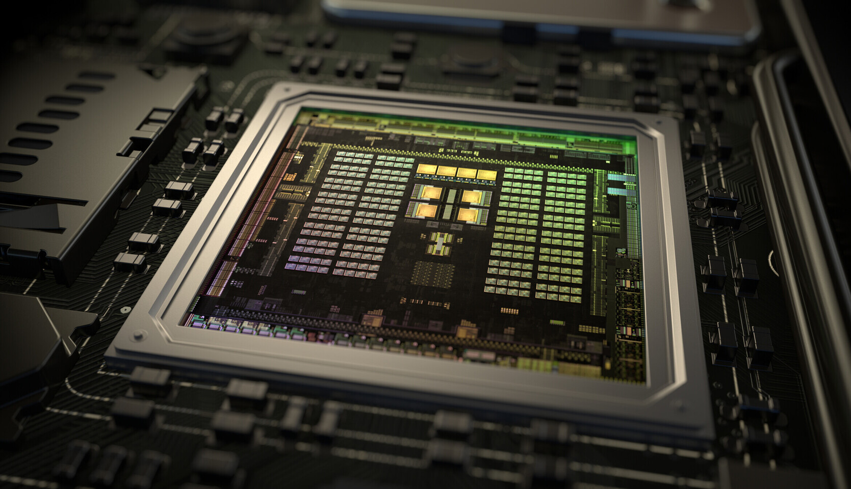
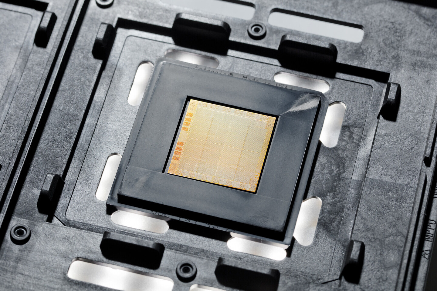
NVIDIA is Preparing Co-Packaged Photonics for NVLink

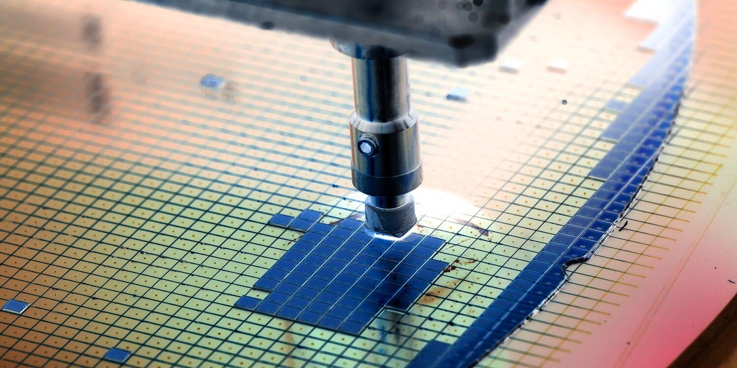
During its GPU Technology Conference (GTC) in China, Mr. Bill Dally—NVIDIA's chief scientist and SVP of research—has presented many interesting things about how the company plans to push the future of HPC, AI, graphics, healthcare, and edge computing. Mr. Dally has presented NVIDIA's research efforts and what is the future vision for its products. Among one of the most interesting things presented was a plan to ditch the standard electrical data transfer and use the speed of light to scale and advance node communication. The new technology utilizing optical data transfer is supposed to bring the power required to transfer by a significant amount.

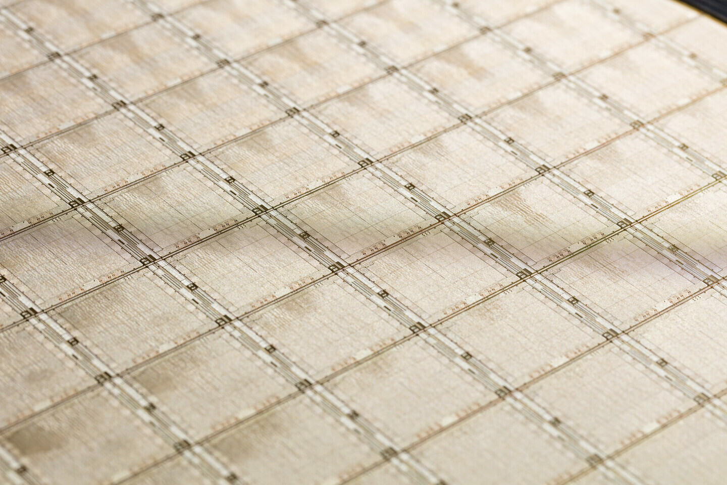
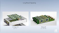
The proposed plan by the company is to use an optical NVLink equivalent. While the current NVLink 2.0 chip uses eight pico Joules per bit (8 pJ/b) and can send signals only to 0.3 meters without any repeaters, the optical replacement is capable of sending data anywhere from 20 to 100 meters while consuming half the power (4 pJ/b). NVIDIA has conceptualized a system with four GPUs in a tray, all of which are connected by light. To power such a setup, there are lasers that produce 8-10 wavelengths. These wavelengths are modulated onto this at a speed of 25 Gbit/s per wavelength, using ring resonators. On the receiving side, ring photodetectors are used to pick up the wavelength and send it to the photodetector. This technique ensures fast data transfer capable of long distances.

AWS and Arm Demonstrate Production-Scale Electronic Design Automation in the Cloud

Today, Amazon Web Services, Inc. (AWS), an Amazon.com, Inc. company, announced that Arm, a global leader in semiconductor design and silicon intellectual property development and licensing, will leverage AWS for its cloud use, including the vast majority of its electronic design automation (EDA) workloads. Arm is migrating EDA workloads to AWS, leveraging AWS Graviton2-based instances (powered by Arm Neoverse cores), and leading the way for transformation of the semiconductor industry, which has traditionally used on-premises data centers for the computationally intensive work of verifying semiconductor designs.

To carry out verification more efficiently, Arm uses the cloud to run simulations of real-world compute scenarios, taking advantage of AWS's virtually unlimited storage and high-performance computing infrastructure to scale the number of simulations it can run in parallel. Since beginning its AWS cloud migration, Arm has realized a 6x improvement in performance time for EDA workflows on AWS. In addition, by running telemetry (the collection and integration of data from remote sources) and analysis on AWS, Arm is generating more powerful engineering, business, and operational insights that help increase workflow efficiency and optimize costs and resources across the company. Arm ultimately plans to reduce its global datacenter footprint by at least 45% and its on-premises compute by 80% as it completes its migration to AWS.

Intel Debuts 2nd-Gen Horse Ridge Cryogenic Quantum Control Chip

At an Intel Labs virtual event today, Intel unveiled Horse Ridge II, its second-generation cryogenic control chip, marking another milestone in the company's progress toward overcoming scalability, one of quantum computing's biggest hurdles. Building on innovations in the first-generation Horse Ridge controller introduced in 2019, Horse Ridge II supports enhanced capabilities and higher levels of integration for elegant control of the quantum system. New features include the ability to manipulate and read qubit states and control the potential of several gates required to entangle multiple qubits.

"With Horse Ridge II, Intel continues to lead innovation in the field of quantum cryogenic controls, drawing from our deep interdisciplinary expertise bench across the Integrated Circuit design, Labs and Technology Development teams. We believe that increasing the number of qubits without addressing the resulting wiring complexities is akin to owning a sports car, but constantly being stuck in traffic. Horse Ridge II further streamlines quantum circuit controls, and we expect this progress to deliver increased fidelity and decreased power output, bringing us one step closer toward the development of a 'traffic-free' integrated quantum circuit."-Jim Clarke, Intel director of Quantum Hardware, Components Research Group, Intel.

TSMC Partners With Google and AMD to Push 3D Silicon

Silicon manufacturing is starting to get harder and harder every day, with new challenges appearing daily. It requires massive investment and massive knowledge to keep a silicon manufacturing company afloat. No company can survive that alone, so some collaborations are emerging. Today, thanks to the sources of Nikkei Asia, we have information that Taiwanese Semiconductor Manufacturing Company (TSMC) is collaborating with Google to push the production of 3D chip manufacturing process, that is said to overcome some of the silicon manufacturing difficulties. The sources also say that AMD is involved in the process as well, making Google and AMD the first customers of the advanced 3D chip design. The two companies are preparing designs for the new way of creating silicon and will help TSMC test and certify the process.

TSMC will deploy the 3D silicon manufacturing technology at its chip packaging plant in Miaoli, which is supposed to do mass production in 2022. With Google and AMD being the first customers of new 3D technology, it is exciting to see what new products will look like and how they will perform. The 3D approach is said to bring huge computing power increase, however, it is a waiting game now to see how it will look like.

Marvell Announces Industry's First 112G 5nm SerDes Solution for Scaling Cloud Data Center Infrastructure

Marvell today unveiled the industry's first 112G 5 nm SerDes solution that has been validated in hardware. The DSP-based SerDes boasts industry-leading performance, power and area, helping to propel 112G as the interconnect of choice for next generation 5G, enterprise, and cloud data center infrastructure. Marvell has recently secured a new custom ASIC design win customer that will embed this new IP to build next generation top-of-rack (ToR) and spine switches for leading hyperscale data centers around the world. The Marvell 5 nm SerDes solution doubles the bandwidth of current systems based on 56G while enabling the deployment of 112G I/Os in many exciting new applications, including network and data center switching, network traffic management, machine learning training and inference, and application-specific accelerators.

Today's news, which comes on the heels of the company's announcement with TSMC of its 5 nm portfolio, further strengthens Marvell's leading data infrastructure offerings in the industry's most advanced process geometry. The 112G 5 nm SerDes solution is part of Marvell's industry-leading IP portfolio that addresses the full spectrum of infrastructure requirements and includes processor subsystems, encryption engines, system-on-chip fabrics, chip-to-chip interconnects, and a variety of physical layer interfaces.

Samsung's 5 nm Node in Production, First SoCs to Arrive Soon

During its Q3 earnings call, Samsung Electronics has provided everyone with an update on its foundry and node production development. In the past year or so, Samsung's foundry has been a producer of a 7 nm LPP (Low Power Performance) node as its smallest node. That is now changed as Samsung has started the production of the 5 nm LPE (Low Power Early) semiconductor manufacturing node. In the past, we have reported that the company struggled with yields of its 5 nm process, however, that seems to be ironed out and now the node is in full production. To contribute to the statement that the new node is doing well, we also recently reported that Samsung will be the sole manufacturer of Qualcomm Snapdragon 875 5G SoC.

The new 5 nm semiconductor node is a marginal improvement over the past 7 nm node. It features a 10% performance improvement that is taking the same power and chip complexity or a 20% power reduction of the same processor clocks and design. When it comes to density, the company advertises the node with x1.33 times increase in transistor density compared to the previous node. The 5LPE node is manufactured using the Extreme Ultra-Violet (EUV) methodology and its FinFET transistors feature new characteristics like Smart Difusion Break isolation, flexible contact placement, and single-fin devices for low power applications. The node is design-rule compatible with the previous 7 nm LPP node, so the existing IP can be used and manufactured on this new process. That means that this is not a brand new process but rather an enhancement. First products are set to arrive with the next generation of smartphone SoCs, like the aforementioned Qualcomm Snapdragon 875.

AMD in Talks with Partners About Custom Radeon RX 6900 XT Designs

Just a few days ago AMD has announced its Radeon RX 6000 series of graphics cards based on the new RDNA 2 architecture. While AMD has given out the "Big Navi" chips to its partners to design custom boards and give users designs with better cooling and possibly higher overclocking capabilities, that doesn't seem to extend to the highest-end parts. So far, we have seen custom designs from companies like ASUS, MSI, etc., and all of them have one thing in common - they only do designs for Radeon RX 6800 or RX 6800 XT. So one would wonder where are the highest-end custom Radeon RX 6900 XT designs.

The first wave of the "custom" cards will be on November 18th, when manufacturers will release designs that are MBA (Made-by-AMD), meaning that the PCB is a reference design, just with a custom cooler installed. When it comes to the custom RX 6900 XT cards, AMD is now in talks with its partners whether to keep the biggest "Big Navi" design available for custom designs, or to keep it as AMD exclusive, with the most likely scenario being the AMD exclusivity. AMD partners could carry the models in their stores and offerings, however, the PCB and cooler design would be AMD's. The situation is yet unresolved so we have to wait and see what comes out of it and if we are getting any custom designs of the Radeon RX 6900 XT model.

Apple A14 SoC Put Under the Microscope; Die Size, and Transistor Density Calculated

Apple has established itself as a master of silicon integrated circuit design and has proven over the years that its processors deliver the best results, generation after generation. If we take a look at the performance numbers of the latest A14 Bionic, you can conclude that its performance is now rivaling some of the x86_64 chips. So you would wonder, what is inside this SoC that makes it so fast? That is exactly what ICmasters, a semiconductor reverse engineering and IP services company, has questioned and decided to find out. For starters, we know that Apple manufactures the new SoCs on TSMC's N5 5 nm node. The Taiwanese company promises to pack 171.3 million transistors per square millimeter, so how does it compare to an actual product?

ICmasters have used electron microscopy to see what the chip is made out of and to measure the transistor density. According to this source, Apple has a chip with a die size of 88 mm², which packs 11.8 billion N5 transistors. The density metric, however, doesn't correspond to that of TSMC. Instead of 171.3 million transistors per mm², the ICmasters measured 134.09 million transistors per mm². This is quite a difference, however, it is worth noting that each design will have it different due to different logic and cache layout.
Apple A14 SoC Die Apple A14 SoC

AMD Updates its Chipset Drivers, Includes Updated Power Plan for Ryzen CPUs

In the anticipation of the AMD Ryzen 5000 series of CPUs launch based on Zen 3 architecture, AMD has just released the updated drivers for its chipsets. Covering a wide selection ranging from B350, A320, X370, X399, B450, X470, X570, B550, and TRX40 Chipset, the updated chipset drivers include some bug fixes and new features. Now there is an updated power plan for AMD Ryzen CPUs that coordinate with chipsets, which means that AMD engineers have developed a new plan for Windows 10 OS which provides the best performance and power usage. You can check out the fixes listed below and you can go to the download link to install the new drivers.
Download: AMD Ryzen Chipset Driver 2.10.13.408.

ASUS Seemingly Drops Support for AMD Ryzen 5000 Series CPUs on X470 Motherboards, the Company Responds

Today there is some quite interesting information circulating the web regarding ASUS and its alleged decision. Going a few months back, AMD released a statement regarding the support for its upcoming Ryzen 5000 series CPUs and said that it should enable compatibility with the last-generation X470 and B450 chipset. That, however, has remained a bit of mystery. The update is baked-in with the BIOS, which every manufacturer, like MSI, ASUS, Gigabyte, etc. provides independently of AMD. So it is a manufacturer-dependant case, where if one vendor chooses not to provide support for 400 series chipsets, many motherboards will not support new CPU generation.

Update Oct 14th: ASUS has reached out to us and said that "ASUS will provide updated BIOS' for the X470 and B450 chipsets based on AMD's current release schedule of new AGESA code in January 2021. This original report was based on incorrect information." This means that the customer support case contained wrong information, and ASUS is going to support 5000 series Ryzen CPUs on 400 series chipsets. Please note that the information below is incorrect.

Arm Highlights its Next Two Generations of CPUs, codenamed Matterhorn and Makalu, with up to a 30% Performance Uplift

Editor's Note: This is written by Arm vice president and general manager Paul Williamson.

Over the last year, I have been inspired by the innovators who are dreaming up solutions to improve and enrich our daily lives. Tomorrow's mobile applications will be even more imaginative, immersive, and intelligent. To that point, the industry has come such a long way in making this happen. Take app stores for instance - we had the choice of roughly 500 apps when smartphones first began shipping in volume in 2007 and today there are 8.9 million apps available to choose from.

Mobile has transformed from a simple utility to the most powerful, pervasive device we engage with daily, much like Arm-based chips have progressed to more powerful but still energy-efficient SoCs. Although the chip-level innovation has already evolved significantly, more is still required as use cases become more complex, with more AI and ML workloads being processed locally on our devices.

NVIDIA Introduces New Family of BlueField DPUs to Bring Breakthrough Networking, Storage and Security Performance to Every Data Center

NVIDIA today announced a new kind of processor—DPUs, or data processing units—supported by DOCA, a novel data-center-infrastructure-on-a-chip architecture that enables breakthrough networking, storage and security performance.

NVIDIA founder and CEO Jensen Huang revealed the company's three-year DPU roadmap in today's GPU Technology Conference keynote. It features the new NVIDIA BlueField -2 family of DPUs and NVIDIA DOCA software development kit for building applications on DPU-accelerated data center infrastructure services.

US Government Could Blacklist Chinese Chipmaker SMIC

The Trump administration has reportedly been considering adding to Chinese chipmaker SMIC (Semiconductor Manufacturing International Corporation) to the trade blacklist of Chinese companies, restricting the company of doing any business with the United States and/or with any of its affiliates. The original report comes from Reuters and it states that the move came from Pentagon after considering whatever SMIC should be placed on a blacklist. It is so far unclear if other US agencies support the decision, however, it should be public in the near future. The company has received the news on Saturday and it was "in complete shock" about the decision. Shortly after the news broke, SMIC stock has fallen as much as 15% amid the possible blacklist. If SMIC would like to continue working with American suppliers, it would need to seek a difficult-to-obtain license from the government.

Update 28th September: The United States government hasofficially imposed sanctions on the Chinese chipmaker SMIC. The company is now under US sanctions and is placed on a trade blacklist.

GLOBALFOUNDRIES Announces New 22FDX+ Platform, Extending FDX Leadership with Specialty Solutions for IoT and 5G Mobility

GLOBALFOUNDRIES (GF ), the world's leading specialty foundry, announced today at its Global Technology Conference the next generation of its FDXTM platform, 22FDX+, to meet the ever-growing need for higher performance and ultra-low power requirements of connected devices. GF's industry-leading 22FDX (22 nm FD-SOI) platform has realized $4.5 billion in design wins, with more than 350 million chips shipped to customers around the world.

GF's new 22FDX+ builds on the company's 22FDX platform, offering a broader set of features that provide high performance, ultra-low power, and specialty features and capabilities for the newest generation of designs. The differentiated offering will further empower customers to create chips that are specifically optimized for Internet of Things (IoT), 5G, automotive, and satellite communications applications.

Arm Announces Next-Generation Neoverse V1 and N2 Cores

Ten years ago, Arm set its sights on deploying its compute-efficient technology in the data center with a vision towards a changing landscape that would require a new approach to infrastructure compute.

That decade-long effort to lay the groundwork for a more efficient infrastructure was realized when we announced Arm Neoverse, a new compute platform that would deliver 30% year-over-year performance improvements through 2021. The unveiling of our first two platforms, Neoverse N1 and E1, was significant and important. Not only because Neoverse N1 shattered our performance target by nearly 2x to deliver 60% more performance when compared to Arm's Cortex-A72 CPU, but because we were beginning to see real demand for more choice and flexibility in this rapidly evolving space.

TSMC 5 nm Node Supply Fully Booked, Apple the Biggest Customer

TSMC has hit a jackpot with its newer nodes like 7 nm and now 5 nm, as the company is working with quite good yields. To boast, TSMC has seen all of its capacity of 7 nm being fully booked by customers like AMD, Apple, and NVIDIA. However, it seems like the company's next-generation 5 nm node is also getting high demand. According to the latest report from DigiTimes, TSMC's N5 5 nm node is fully booked to the end of 2020. And the biggest reason for that is the biggest company in the world - Apple. Since Apple plans to launch the next-generation iPhone, iPad, and Arm-based MacBook, the company has reportedly booked most of the 5 nm capacity for 2020, meaning that there are lots of chips that Apple will consume. TSMC can't be dependent only on one company like Apple, so the smaller portion of capacity went to other customers as well.

SiFive To Introduce New RISC-V Processor Architecture and RISC-V PC at Linley Fall Virtual Processor Conference

SiFive, Inc., the leading provider of commercial RISC-V processor IP and silicon solutions, today announced that Dr. Yunsup Lee, CTO of SiFive, and Dr. Krste Asanovic, Chief Architect of SiFive, will present at the technology industry's premier processor conference, the Linley Fall Virtual Processor Conference. The conference will be held on October 20th - 22nd and 27th - 29th, 2020 and will feature high-quality technical content from leading semiconductor companies worldwide.

"Industry demand for AI performance has skyrocketed over the last few years driven by rapid adoption from the data center to the edge. This year's Linley Fall Processor Conference will feature our biggest program yet and will introduce a host of new technology disclosures and product announcements of innovative processor architectures and IP technologies," said Linley Gwennap, principal analyst and conference chairperson. "In spite of the challenges posed by the pandemic, development of these technologies continues to accelerate and we're excited to be sharing these presentations with a global audience via our live-streamed format."

NVIDIA CEO Jensen Huang Says NVIDIA-Branded CPUs Could be Coming

It was just yesterday that we have received the news of NVIDIA's latest move - acquiring Arm Ltd. from Softbank Group for $40 billion. However, it seems like there are more reasons for the deal than what meets the eye. In the briefing regarding the acquisition, NVIDIA's CEO was asked a question, by Timothy Prickett Morgan, from TheNextPlatform, about NVIDIA's plans for a possible implementation of Arm's Neoverse core in an NVIDIA-branded CPU design and start selling them to data centers. To that question, Mr. Huang gave a prolonged answer indirectly saying that the company can build the CPU if there is a market for it.

He explains that there is an entire network surrounding the Arm ecosystem and that there may be customers interested in contracting NVIDIA to build them semi-custom or completely custom chip based on Arm ISA on NVIDIA's own interest. Any of these options are available and Mr. Haung says that they are there for the best interest of the ecosystem to enrich it enhance it even further. This means that it is just a matter of time before we see NVIDIA-branded CPU make its way to data-center or some other areas of technology, so we have to wait and see for ourselves.

Samsung and SK Hynix to Impose Sanctions Against Huawei

Ever since the Trump administration imposed sanctions against Huawei to stop it from purchasing parts from third-party vendors to bypass the ban announced back in May, some vendors continued to supply the company. So it seems like some Korean manufacturers will be joining the doings of the US government, and apply restrictions to Huawei. According to the reports of South Korean media outlets, Samsung Electronics and SK Hynix will be joining the efforts of the US government and the Trump administration to impose sanctions against Chinese technology giant - Huawei.

It is reported that on September 15th, both Samsung and SK Hynix will stop any shipments to Huawei, where Samsung already stopped efforts for creating any new shipments. SK Hynix is said to continue shipping DRAM and NAND Flash products until September 14th, a day before the new sanctions are applied. Until the 14th, Huawei will receive some additional chips from SK Hynix. And it is exactly SK Hynix who is said to be a big loser here. It is estimated that 41.2% of SK Hynix's H1 2020 revenue came from China, most of which was memory purchased for Huawei phones and tablets. If the company loses Huawei as a customer, it would mean that the revenue numbers will be notably lower.

COVID-19 Drives Rise in Global Fab Equipment Spending, SEMI Reports

Soaring pandemic-inspired demand for chips that power everything from communications and IT infrastructures to personal computing, gaming and healthcare electronics will drive an 8% increase in global fab equipment spending in 2020 and a 13% increase in 2021, SEMI announced today in its World Fab Forecast report. Rising demand for semiconductors for datacenter infrastructures and server storage along with the buildup of safety stock as U.S.-China trade tensions intensify are also contributing to this year's growth.

The bullish trend for overall fab equipment investments comes as the semiconductor industry recovers from a 9% decline in fab spending in 2019 and navigates a roller-coaster 2020 with actual and projected spending drops in the first and third quarters mixed with second- and fourth-quarter increases. See figure below:

Arm and DARPA Sign Partnership Agreement to Accelerate Technological Innovation

Arm today announced a three-year partnership agreement with the U.S. Defense Advanced Research Projects Agency (DARPA), establishing an access framework to all commercially available Arm technology. With DARPA's Electronics Resurgence Initiative gaining momentum, the new agreement will enable the research community that supports DARPA's programs to quickly and easily take advantage of Arm's leading IP, tools and support, accelerating innovation in a variety of fields.

"The span of DARPA research activity opens up a huge range of opportunities for future technological innovation," said Rene Haas, president, IP Products Group, Arm. "Our expanded DARPA partnership will provide them with access to the broadest range of Arm technology to develop compute solutions supported by the world's largest ecosystem of tools, services and software."

Apple A14X Bionic Rumored To Match Intel Core i9-9880H

The Apple A14X Bionic is an upcoming processor from Apple which is expected to feature in the upcoming iPad Pro models and should be manufactured on TSMC's 5 nm node. Tech YouTuber Luke Miani has recently provided a performance graph for the A14X chip based on "leaked/suspected A14 info + average performance gains from previous X chips". In these graphs, the Apple A14X can be seen matching the Intel Core i9-9880H in Geekbench 5 with a score of 7480. The Intel Intel Core i9-9880H is a 45 W eight-core mobile CPU found in high-end notebooks such as the 2019 16-inch MacBook Pro and requires significant cooling to keep thermals under control.

If these performance estimates are correct or even close then Apple will have a serious productivity device and will serve as a strong basis for Apple's transition to custom CPU's for it's MacBook's in 2021. Apple may use a custom version of the A14X with slightly higher clocks in their upcoming ARM MacBooks according to Luke Miani. These results are estimations at best so take them with a pinch of salt until Apple officially unveils the chip.

Raja Koduri Previews "PetaFLOPs Scale" 4-Tile Intel Xe HP GPU

Raja Koduri, Intel's chief architect and senior vice president of Intel's discrete graphics division, has today held a talk at HotChips 32, the latest online conference of 2020, that shows off the latest architectural advancements in the semiconductor industry. So Intel has prepared two talks, one about Ice Lake-SP server CPUs and one about Intel's efforts in the upcoming graphics card launch. So what has Intel been working on the whole time? Raja Koduri took over the talk and has benchmarked the upcoming GPU and recorded how much raw power the GPUs posses, possibly counting in PetaFLOPs.

When Mr. Koduri got to talk, he pulled the 4-tile Xe HP GPU out of his pocket and showed for the first time how the chip looks. And it is one big chip. Featuring 4 tiles, the GPU represents Intel's fastest and biggest variant of Xe HP GPUs. The benchmark Intel ran was made to show off scaling on the Xe architecture and how the increase in the number of tiles results in a scalable increase in performance. Running on a single tile, the GPU managed to develop the performance of 10588 GFLOPs or around 10.588 TeraFLOPs. When there are two tiles, the performance scales almost perfectly at 21161 GFLOPS (21.161 TeraFLOPs) for 1.999X improvement. At four tiles the GPU achieves 3.993 times scaling and scores 41908 GFLOPs resulting in 41.908 TeraFLOPS, all measured in single-precision FP32.
Intel Xe HP GPU Demo Intel Xe HP GPU Demo Intel Xe HP GPU Demo

IBM Reveals Next-Generation IBM POWER10 Processor

IBM today revealed the next generation of its IBM POWER central processing unit (CPU) family: IBM POWER10. Designed to offer a platform to meet the unique needs of enterprise hybrid cloud computing, the IBM POWER10 processor uses a design focused on energy efficiency and performance in a 7 nm form factor with an expected improvement of up to 3x greater processor energy efficiency, workload capacity, and container density than the IBM POWER9 processor.

Designed over five years with hundreds of new and pending patents, the IBM POWER10 processor is an important evolution in IBM's roadmap for POWER. Systems taking advantage of IBM POWER10 are expected to be available in the second half of 2021. Some of the new processor innovations include:
IBM POWER10 Processor IBM POWER10 Processor

Qualcomm Could Deliver Chips to Huawei

In the ave of the news that Trump administration has forbidden TSMC to have Huawei as its customer, Huawei seems to be exploring new options for sourcing the best performing mobile processors. As the company has turned to the Chinese SMIC semiconductor factory, it still needs a backup plan in the case of Chinese semiconductor manufacturing flops. So to combat US sanctions, Huawei will use already made chips form the US company - Qualcomm. By sourcing the processors from Qualcomm, Huawei is losing some benefits of customs design like better system integration, however, it will gain quite powerful mobile processors. As Qualcomm is known for providing the fastest processors for Android smartphones, Huawei has ensured that it remains competitive. Qualcomm is reportedly now negotiating with the US government about delivering the chips to Huawei, and if it is allowed, Qualcomm will gain a big customer.
Return to Keyword Browsing
May 21st, 2024 07:36 EDT change timezone

New Forum Posts

Popular Reviews

Controversial News Posts