News Posts matching #chip

Return to Keyword Browsing

AMD Announces New Model Numbers for Future Mobile Processors

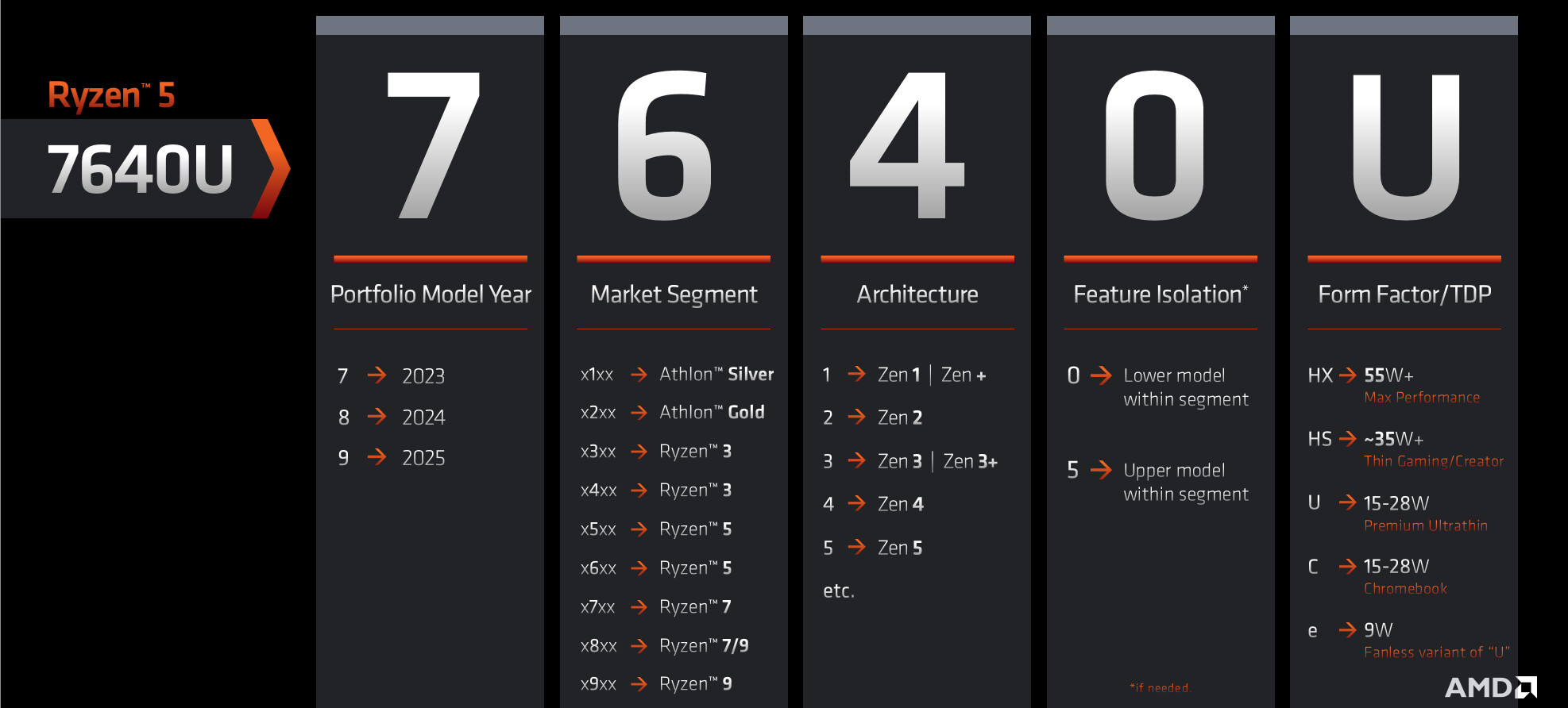
Starting next year, AMD will move to a new model number scheme for its mobile processors and it appears that the company has decided to use the first digit to represent the model year, which should alleviate some past confusion. The second digit in the model name will represent where in the product stack the specific chip will sit and here we're potentially getting some new 6 and 8 models, although nothing guarantees that AMD will actually implement these segments into real products. The third digit represents the architecture, so a four equals Zen 4 for example.

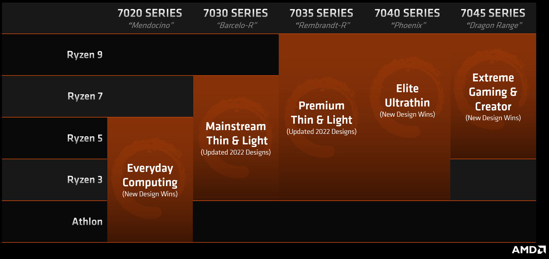
The last digit in the model names is a new addition where AMD has sub SKUs that offer some performance advantage of the base SKU of a specific model and this digit will apparently only be represented by a 0 or a 5. Finally AMD has added a new suffix too, where C stands for Chromebook. This translates to 15-28 Watt chips that have been designed specifically for Chromebook usage. The current HX, HS and U suffix lettering will carry over, alongside the lower-case e for 9 W versions the U SKUs. AMD has also segmented it's mobile CPUs according to the chart below, to try and deliver a clearer use case for its various CPU models. The chart is pretty self explanatory, although some of the segmentation will apply to updated models of current designs, whereas others will only apply to new laptop designs. The new model numbering scheme will apply to at least 2025.

TSMC has Seven Major Customers Lined Up for its 3 nm Node

Based on media reports out of Taiwan, TSMC seems to have plenty of customers lined up for its 3 nm node, with Apple being the first customer out the gates when production starts sometime next month. However, TSMC is only expected to start the production with a mere 1,000 wafer starts a month, which seems like a very low figure, especially as this is said to remain unchanged through all of Q4. On the plus side, yields are expected to be better than the initial 5 nm node yields. Full-on mass production for the 3 nm node isn't expected to happen until the second half of 2023 and TSMC will also kick off its N3E node sometime in 2023.

Apart from Apple, major customers for the 3 nm node include AMD, Broadcom, Intel, MediaTek, NVIDIA and Qualcomm. Contrary to earlier reports by TrendForce, it appears that TSMC will continue its rollout of the 3 nm node as previously planned. Apple is expected to produce the A17 smartphone and tablet SoC, as well as advanced versions of the M2, as well as the M3 laptop and desktop processors on the 3 nm node. Intel is still said to be producing its graphics chiplets with TSMC, with the potential for GPU and FPGA products in the future. There's no word on what the other customers are planning to produce on the 3 nm node, but MediaTek and Qualcomm are obviously looking at using the node for future smartphone and tablet SoCs, with AMD and NVIDIA most likely aiming for upcoming GPUs and Broadcom for some kind of HPC related hardware.

Tachyum Submits Bid for 20-Exaflop Supercomputer to U.S. Department of Energy Advanced Computing Ecosystems

Tachyum today announced that it has responded to a U.S. Department of Energy Request for Information soliciting Advanced Computing Ecosystems for DOE national laboratories engaged in scientific and national security research. Tachyum has submitted a proposal to create a 20-exaflop supercomputer based on Tachyum's Prodigy, the world's first universal processor.

The DOE's request calls for computing systems that are five to 10 times faster than those currently available and/or that can perform more complex applications in "data science, artificial intelligence, edge deployments at facilities, and science ecosystem problems, in addition to the traditional modeling and simulation applications."

More Details Emerge on Mediatek's Intel Foundry Plans

Last week's news about Mediatek signing an agreement to use Intel's Foundry Services (IFS) led to some speculation as to what Mediatek would be manufacturing at IFS. Details have now emerged in the Taiwan press about Mediatek's plans and the first products will be using the Intel 16 process, what was previously known as its 22 nm node. As such, we're not talking about anything cutting edge or even remotely close, but that's hardly a problem for Mediatek, as the company makes a vast range of products suitable for the node.

MediaTek CEO Rick Tsai mentioned that IFS will be used for producing semiconductors for digital TVs and wireless access networks at an investor conference in Taiwan. This suggests that most of the components might not even be for Mediatek itself, but rather its subsidiaries, such as MStar or Airoha. MStar is a company that produces a wide range of lower-end smart TV chips, whereas Airoha has ended up taking over Mediatek's networking and Bluetooth business units. Admittedly, Mediatek still has some of these types of products under its own brand, but these tend to be higher-end products that would require a more advanced node than 22 nm in most cases. Mediatek's move to IFS has raised concerns in Taiwan that the smaller foundries might be losing business from Mediatek over time, which means that UMC and PSMC are going to be on the losing end of this deal.

US Congress Passes the CHIPS and Science Act

As The CHIPS and Science Act of 2022 heads to President Biden's desk for his signature, following its passage in Congress, OSTP's Dr. Alondra Nelson is releasing the following statement: "The bipartisan CHIPS and Science Act of 2022 is the most significant American investment in science, technology, and innovation in a generation. It will revitalize and advance U.S. leadership in science and technology, spur U.S. competitiveness and economic development, and bolster our domestic semiconductor supply chains. Most important, it will deliver opportunities for Americans all across the nation.

For working Americans, the stakes of this legislation could not be higher. Semiconductor chips power our daily lives, from the telecommunications that keep us all connected, and medical devices that keep our loved ones alive, to financial institutions that help secure our families' futures, and the computers from which millions of Americans run their businesses. They are a door to a future of innovation, progress, and economic security.

Airoha Sets 10-year Milestone with Bluetooth LE Audio Certification

Airoha Technology today announced that its new series of Bluetooth audio chips have successfully completed the latest Bluetooth Low Energy Audio Qualification Process. This is one of the most important R&D achievements of its Bluetooth audio R&D team consisted of hundreds of engineers, who continues to revolutionize the wireless audio end device market. The "flagship" and "professional" series of chipsets support LE audio and Bluetooth 5.3 for multiple applications such as True Wireless Stereo (TWS) earbuds, Bluetooth smart speakers, assistive listening devices, and Bluetooth transmitters. The products are currently being tested by many brand customers and are expected to be available worldwide in the first half of 2023.

"The LE Audio specifications are the most important milestone reached in the Bluetooth audio industry in the past decade. With the support of our strong R&D team consisting of hundreds of engineers who have accumulated nearly a decade of technical expertise, Airoha became one of the world's first certified chip providers. This supports many customers to accelerate the launch of their end devices. The wireless audio innovation brought by the latest Bluetooth LE technology will expedite the process by which consumers and businesses enjoy the convenient and innovative services it brings, fully demonstrating the Airoha's vision and business philosophy." said Yuchuan Yang, Sr. Vice President of Airoha.

Intel and MediaTek Form Foundry Partnership

Intel and MediaTek today announced a strategic partnership to manufacture chips using Intel Foundry Services' (IFS) advanced process technologies. The agreement is designed to help MediaTek build a more balanced, resilient supply chain through the addition of a new foundry partner with significant capacity in the United States and Europe. MediaTek plans to use Intel process technologies to manufacture multiple chips for a range of smart edge devices. IFS offers a broad manufacturing platform with technologies optimized for high performance, low power and always-on connectivity built on a roadmap that spans production-proven three-dimensional FinFET transistors to next-generation breakthroughs.

"As one of the world's leading fabless chip designers powering more than 2 billion devices a year, MediaTek is a terrific partner for IFS as we enter our next phase of growth," said IFS President Randhir Thakur. "We have the right combination of advanced process technology and geographically diverse capacity to help MediaTek deliver the next billion connected devices across a range of applications."

TikTok's Parent Company ByteDance Starts Developing Custom Processors

TikTok's parent company ByteDance has recently begun hiring chip designers to help develop specialized processors for fields where they haven't been able to find existing suppliers. The company is looking to design chips that are optimized for hosting their video, information, and entertainment apps without any plans to sell these processors to other companies. This latest announcement follows various other Chinese companies such as Alibaba and Baidu in developing custom processors to decrease their reliance on foreign companies and improve performance in specific tasks. The initial job listings only include 31 openings for positions such as experts, specialists, and interns with more staff likely required in the future.

Qualcomm Launches Snapdragon W5+ and W5 Platforms for Next Generation Wearables

Qualcomm Technologies, Inc. today unveiled the latest additions to the company's suite of premium wearable platforms, Snapdragon W5+ Gen 1 and Snapdragon W5 Gen 1. These platforms are designed to advance ultra-low power and breakthrough performance for next generation connected wearables with a focus on extended battery life, premium user experiences, and sleek, innovative designs. By using these platforms, manufacturers can scale, differentiate, and develop products faster in the continuously growing and segmenting wearables industry.

New enhancements to the flagship Snapdragon W5+ platform offer 50% lower power, 2X higher performance, 2X richer features, and 30% smaller size, compared to our previous generation, enabling wearable manufacturers to deliver the differentiated experiences consumers demand. Based on the hybrid architecture, the purpose-built platform is comprised of a 4 nm-based system-on-chip and 22 nm-based highly integrated always-on co-processor. It incorporates a series of platform innovations including new ultra-low power Bluetooth 5.3 architecture, low power islands for Wi-Fi, GNSS, and Audio, and low power states such as Deep Sleep and Hibernate.

STMicroelectronics and GlobalFoundries to advance FD-SOI ecosystem with new 300mm manufacturing facility in France

STMicroelectronics, a global semiconductor leader serving customers across the spectrum of electronics applications, and GlobalFoundries Inc., a global leader in feature-rich semiconductor manufacturing, today announced they have signed a Memorandum of Understanding to create a new, jointly-operated 300 mm semiconductor manufacturing facility adjacent to ST's existing 300 mm facility in Crolles, France. This facility is targeted to ramp at full capacity by 2026, with up to 620,000 300 mm wafer per year production at full build-out (~42% ST and ~58% GF).

ST and GF are committed to building capacity for their European and global customer base. This new facility will support several technologies, in particular FD-SOI-based technologies, and will cover multiple variants. This includes GF's market leading FDX technology and ST's comprehensive technology roadmap down to 18 nm, which are expected to remain in high demand for Automotive, IoT, and Mobile applications for the next few decades. FD-SOI technology has origins in the Grenoble (France) area. It has been part of ST technology and product roadmap in its Crolles facility since the early beginnings, and it was later enabled with differentiation and commercialized for manufacturing at GF's Dresden facility. FD-SOI offers substantial benefits for designers and customers, including ultra-low power consumption as well as easier integration of additional features such as RF connectivity, mmWave and security.

Semiconductor Fab Order Cancellations Expected to Result in Reduced Capacity Utilization Rate in 2H22

According to TrendForce investigations, foundries have seen a wave of order cancellations with the first of these revisions originating from large-size Driver IC and TDDI, which rely on mainstream 0.1X μm and 55 nm processes, respectively. Although products such as MCU and PMIC were previously in short supply, foundries' capacity utilization rate remained roughly at full capacity through their adjustment of product mix. However, a recent wave cancellations have emerged for PMIC, CIS, and certain MCU and SoC orders. Although still dominated by consumer applications, foundries are beginning to feel the strain of the copious order cancellations from customers and capacity utilization rate has officially declined.

Looking at trends in 2H22, TrendForce indicates, in addition to no relief from the sustained downgrade of driver IC demand, inventory adjustment has begun for smartphones, PCs, and TV-related peripheral components such as SoCs, CIS, and PMICs, and companies are beginning to curtail their wafer input plans with foundries. This phenomenon of order cancellations is occurring simultaneously in 8-inch and 12-inch fabs at nodes including 0.1X μm, 90/55 nm, and 40/28 nm. Not even the advanced 7/6 nm processes are immune.

Samsung Adopts Ansys' Simulation Portfolio to Create Semiconductor Designs to Optimize High-Speed Connectivity

Samsung Foundry will engage Ansys' industry-leading electromagnetic (EM) simulation tools to develop ultramodern designs, including 5G/6G, on the most advanced chips, nodes, and process technologies. Ansys' simulation solutions will deliver a comprehensive EM-aware design flow with greater capacity, speed, and integration capabilities for Samsung's most advanced semiconductor technology, accelerating on-chip design cycle times to boost high-speed connectivity while helping to reduce design error and risk.

Samsung designers will leverage Ansys' EM design tools, Ansys RaptorX, Ansys VeloceRF, and Ansys Exalto, to help reduce time to market by two to three weeks on smaller designs and up to two months for complex designs. With automation capabilities that optimize calculations and modeling, coupled with larger capacity, Ansys' software will allow the Samsung team to design at faster speeds with higher fidelity.

Mobileye Launches EyeQ Kit: New SDK for Advanced Safety and Driver-Assistance Systems

Mobileye, an Intel company, has launched the EyeQ Kit - its first software development kit (SDK) for the EyeQ system-on-chip that powers driver-assistance and future autonomous technologies for automakers worldwide. Built to leverage the powerful and highly power-efficient architecture of the upcoming EyeQ 6 High and EyeQ Ultra processors, EyeQ Kit allows automakers to utilize Mobileye's proven core technology, while deploying their own differentiated code and human-machine interface tools on the EyeQ platform.

"EyeQ Kit allows our customers to benefit from the best of both worlds — Mobileye's proven and validated core technologies, along with their own expertise in delivering unique driver experiences and interfaces. As more core functions of vehicles are defined in software, we know our customers will want the flexibility and capacity they need to differentiate and define their brands through code."
- Prof. Amnon Shashua, Mobileye president and chief executive officer

Samsung Begins Chip Production Using 3nm Process Technology With GAA Architecture

Samsung Electronics, the world leader in semiconductor technology, today announced that it has started initial production of its 3-nanometer (nm) process node applying Gate-All-Around (GAA) transistor architecture. Multi-Bridge-Channel FET (MBCFET), Samsung's GAA technology implemented for the first time ever, defies the performance limitations of FinFET, improving power efficiency by reducing the supply voltage level, while also enhancing performance by increasing drive current capability. Samsung is starting the first application of the nanosheet transistor with semiconductor chips for high performance, low power computing application and plans to expand to mobile processors.

"Samsung has grown rapidly as we continue to demonstrate leadership in applying next-generation technologies to manufacturing, such as foundry industry's first High-K Metal Gate, FinFET, as well as EUV. We seek to continue this leadership with the world's first 3 nm process with the MBCFET," said Dr. Siyoung Choi, President and Head of Foundry Business at Samsung Electronics. "We will continue active innovation in competitive technology development and build processes that help expedite achieving maturity of technology."

MediaTek Announces Commitment to Open New Semiconductor Design Center at Purdue University in Indiana

Today, leading global fabless chipmaker MediaTek Inc., [joined by Indiana Governor Eric J. Holcomb, Deputy Secretary of Commerce Don Graves, Indiana Secretary of Commerce Bradley B. Chambers, and Purdue College of Engineering's Dr. Mung Chiang] announced their commitment to accept a state transition assistance package from the Indiana Economic Development Commission (IEDC) to support its very first Midwest semiconductor chip design center in West Lafayette, Indiana. MediaTek also shared its intention to create a new research partnership with Purdue to collaborate on engineering talent development and new research on next-generation computing and communications chip design. The news was shared with senior leaders, other international investors and policymakers assembled in National Harbor, Maryland for the 2022 SelectUSA Investment Summit.

This novel partnership in Indiana represents a new U.S. growth model for MediaTek USA; outside the traditional centers of gravity for chip design. "We believe strongly that being in Indiana means we'll have access to some of the best engineering talent in the world," said Dr. Kou-Hung Lawrence Loh, Corporate Senior Vice President of MediaTek Inc. and President of MediaTek USA, Inc. "Not just at Purdue, but West Lafayette is only four hours away from nearly a dozen of the top engineering schools in the country. In the post pandemic world, top candidates tell us they want to be closer to home, near family and they want to have a real house and great schools. Indiana offers all that and more."

Intel Labs Announces Integrated Photonics Research Advancement

Intel Labs announces a significant advancement in its integrated photonics research - the next frontier in increasing communication bandwidth between compute silicon in data centers and across networks. The latest research features industry-leading advancements in multiwavelength integrated optics, including the demonstration of an eight-wavelength distributed feedback (DFB) laser array that is fully integrated on a silicon wafer and delivers excellent output power uniformity of +/- 0.25 decibel (dB) and wavelength spacing uniformity of ±6.5% that exceed industry specifications.

"This new research demonstrates that it's possible to achieve well-matched output power with uniform and densely spaced wavelengths. Most importantly, this can be done using existing manufacturing and process controls in Intel's fabs, thereby ensuring a clear path to volume production of the next-generation co-packaged optics and optical compute interconnect at scale." -Haisheng Rong, senior principal engineer at Intel Labs

Iceotope collaborates with Intel and HPE to accelerate sustainability and cut power for Edge and Data Center compute requirements by up to 30 Percent

Iceotope, the global leader in Precision Immersion Cooling, has announced that its chassis-level cooling system is being demonstrated in the Intel Booth at HPE Discover 2022, the prestigious "Edge-to-cloud Conference". Ku:l Data Center is the product of a close collaboration between Iceotope, Intel and HPE and promises a faster path to net zero operations by reducing edge and data center energy use by nearly a third. Once the sole preserve of arcane, high performance computing applications, liquid cooling is increasingly seen as essential technology for reliable and efficient operations of any IT load in any location. There is a pressing concern about sustainability impacts as distributed edge computing environments proliferate to meet the demand for data processing nearer the point of use, as well as growing facility power and cooling consumption driven by AI augmentation and hotter chips.

Working together with Intel and HPE, Iceotope benchmarked the power consumption of a sample IT installation being cooled respectively using air and precision immersion liquid cooling. The results show a substantial advantage in favour of liquid cooling, reducing overall power use across IT and cooling infrastructure.

AMD Instinct MI300 APU to Power El Capitan Exascale Supercomputer

The Exascale supercomputing race is now well underway, as the US-based Frontier supercomputer got delivered, and now we wait to see the remaining systems join the race. Today, during 79th HPC User Forum at Oak Ridge National Laboratory (ORNL), Terri Quinn at Lawrence Livermore National Laboratory (LLNL) delivered a few insights into what El Capitan exascale machine will look like. And it seems like the new powerhouse will be based on AMD's Instinct MI300 APU. LLNL targets peak performance of over two exaFLOPs and a sustained performance of more than one exaFLOP, under 40 megawatts of power. This should require a very dense and efficient computing solution, just like the MI300 APU is.

As a reminder, the AMD Instinct MI300 is an APU that combines Zen 4 x86-64 CPU cores, CDNA3 compute-oriented graphics, large cache structures, and HBM memory used as DRAM on a single package. This is achieved using a multi-chip module design with 2.5D and 3D chiplet integration using Infinity architecture. The system will essentially utilize thousands of these APUs to become one large Linux cluster. It is slated for installation in 2023, with an operating lifespan from 2024 to 2030.

Off-season Offsets Wafer Pricing Increase, 1Q22 Foundry Output Value Up 8.2% QoQ, Says TrendForce

According to TrendForce research, although demand for consumer electronics remains weak, structural growth demand in the semiconductor industry including for servers, high-performance computing, automotive, and industrial equipment has not flagged, becoming a key driver for medium and long term foundry growth. At the same time, due to robust wafer production at higher pricing in 1Q22, quarterly output value hit a new high for the 11th consecutive quarter, reaching US$31.96 billion, 8.2% QoQ, marginally less than the previous quarter. In terms of ranking, the biggest change is Nexchip surpassed Tower at the ninth position.

TSMC's across the board wafer hikes in 4Q21 on batches primarily produced in 1Q22 coupled with sustained strong demand for high-performance computing and better foreign currency exchange rates pushed TSMC's 1Q22 revenue to $17.53 billion, up 11.3% QoQ. Quarterly revenue growth by node was generally around 10% and the 7/6 nm and 16/12 nm processes posted the highest growth rate due to small expansions in production. The only instance of revenue decline came at the 5/4 nm process due to Apple's iPhone 13 entering the off season for production stocking.

NVIDIA RTX 40 Series Could Reach 800 Watts on Desktop, 175 Watt for Mobile/Laptop

Rumors of NVIDIA's upcoming Ada Lovelace graphics cards keep appearing. With every new update, it seems like the total power consumption is getting bigger, and today we are getting information about different SKUs, including mobile and desktop variants. According to a well-known leaker, kopite7kimi, we have information about the power limits of the upcoming GPUs. The new RTX 40 series GPUs will feature a few initial SKUs: AD102, AD103, AD104, and AD106. Every SKU, except the top AD102, will be available as well. The first in line, AD102, is the most power-hungry SKU with a maximum power limit rating of 800 Watts. This will require multiple power connectors and a very beefy cooling solution to keep it running.

Going down the stack, we have an AD103 SKU limited to 450 Watts on desktop and 175 Watts on mobile. The AD104 chip is limited to 400 Watts on desktop, while the mobile version is still 175 Watts. Additionally, the AD106 SKU is limited to 260 Watts on desktop and 140 Watts on mobile.

GlobalFoundries and STMicroelectronics Considering a New Fab in France

Recent news suggests that TSMC isn't too interested in setting up a fab in Europe, but it appears there are other interested parties that are now courting the EU, namely a potential joint venture between GlobalFoundries and STMicroelectronics. The two companies are hoping to get a slice of the same cake as Intel, namely the European Chips Act, to help subsidise the cost of the proposed fab. Although GlobalFoundries are headquartered in New York and STMicroelectronics in Geneva, the latter being a French-Italian conglomerate, the planned location for the new fab will be somewhere in France.

It's highly unlikely that this will be a cutting edge or even a leading edge fab, as neither company is in the business of producing products in those market segments. ST makes a wide range of chips from MCUs and other types of microprocessors, to specialised memory products, a wide range of sensors, MEMS based devices and all kinds of electronics for electrical vehicles, as well as highly specialised components for the space industry. GloFo obviously stepped off the competitive foundry ladder some years ago and have been focusing on specialised processes and nodes since then, such as FD-SOI, a technology, something the two companies announced a joint partnership around earlier this year. As such, it's likely that this potential fab will focus on making parts needed for the automotive industry in Europe, among other things. There's still a long way to go and neither company has made any kind of official statement about the potential partnership as yet.

Japan and the US Joins Forces to Produce 2 nm Chips in Japan by 2025

Based on a report by the Nikkei, Japan and the US have joined forces to speed up the development of semiconductor production at 2 nm nodes in Japan by 2025. It's not exactly clear how this is going to happen, but the two nations are said to have signed a bilateral chip technology partnership. The heavy lifting is said to be done by private companies from both nations, but in terms of research and actual chip production. Part of the reason for the move, is that Japan wants to be able to manufacture cutting edge ICs domestically for next-generation chips.

The research is said to be kicking off as soon as this summer, although no decisions have been made with regards to the manufacturing structure, with the Nikkei suggesting two alternatives, based on information from the Japanese Ministry of Economy. There will either be a joint partnership between Japanese and US businesses, or it could be a wholly Japanese owned setup. It appears that one major reason for this project is the production of ICs for the Japanese defence industry, as advanced electronics are needed in a lot of related products, ranging from fighter jets and missiles, to radar systems and communication systems. However, the article also suggests that the 2 nm node is suitable for everything from components for quantum computers to smartphones. Japan already makes advanced silicon wafers and many other parts and components used in semiconductor manufacturing, but the nation has fallen behind in the actual manufacturing of leading edge semiconductors over the past few years.

AMD set to Open Manufacturing Plant in Malaysia in Early 2023

AMD's Malaysian joint venture, TF-AMD Microelectronics is in the middle of the construction of a US$452 million manufacturing plant on the island of Penang off the west coast of Malaysia. The facility itself is said to cover 139,000 square metres and is said to create some 3,000 jobs related to advanced semiconductor engineering. The new plant will bring TF-AMD's total manufacturing space in Penang to 210,000 square metres, as the company already has a prior facility on the island.

The plant will allow AMD to expand the chip packaging side of its business, something that is going to be key for many of its future products, considering AMD appears to be focusing on manufacturing a wider range of chips that are made up from multiple chiplets. The TF in the name stands for TongFu, which is a Chinese IC assembly and testing company that AMD has partnered up with in Malaysia. The current plant does everything from wafer sorting to wafer level chip scale packaging to final testing and AMD chips made in Malaysia would have been assembled here.

Apple M1 Chips Affected by Unpatchable "PACMAN" Exploit

Apple M1 chips are a part of the Apple Silicon family that represents a new transition to Arm-based cores with new power and performance targets for Apple devices. A portion of building a processor is designing its security enclave, and today we have evidence that M1 processors got a new vulnerability. The PACMAN is a hardware attack that can bypass Pointer Authentication (PAC) on M1 processors. Security researchers took an existing concept of Spectre and its application in the x86 realm and now applied it to the Arm-based Apple silicon. PACMAN exploits a current software bug to perform pointer authentication bypass, which may lead to arbitrary code execution.

The vulnerability is a hardware/software co-design that exploits microarchitectural construction to execute arbitrary codes. PACMAN creates a PAC Oracle to check if a specific pointer matches its authentication. It must never crash if an incorrect guess is supplied and the attack brute-forces all the possible PAC values using the PAC Oracle. To suppress crashes, PAC Oracles are delivered speculatively. And to learn if the PAC value was correct, researchers used uArch side channeling. In the CPU resides translation lookaside buffers (TLBs), where PACMAN tries to load the pointer speculatively and verify success using the prime+probe technique. TLBs are filled with minimal addresses required to supply a particular TLB section. If any address is evicted from the TLB, it is likely a load success, and the bug can take over with a falsely authenticated memory address.
Apple M1 PACMAN Attack

TSMC Forecasts 30 Percent Increase in Sales for 2022

In 2021 TSMC saw an increase in sales of 24.9 percent in monetary value, but for 2022, the company is expecting this figure to reach somewhere around the 30 percent mark. For this quarter alone, TSMC is expecting a revenue of somewhere between US$17.6 to US$18.2 billion, with a gross margin ending up as high as 58 percent. Despite the positive outlook, TSMC hasn't been doing well on the Taiwanese stock exchange this year, as the company has lost more than a tenth of its value in 2022.

That said, TSMC is pressing forward and will still be spending in excess of US$40 billion in 2023 to expand its production capacity, following the US$40 to US$44 billion it will invest this year. The company isn't overly concerned about inflation at this point in time either, saying it doesn't have a direct impact on the semiconductor industry. TSMC is seeing a slowdown in the consumer chip space, but it's seeing an uptick in business when it comes to EV related ICs. TSMC's production lines are at full utilisation for at least the rest of 2022, but most likely long into 2023.
Return to Keyword Browsing
May 21st, 2024 12:28 EDT change timezone

New Forum Posts

Popular Reviews

Controversial News Posts