News Posts matching #chip

Return to Keyword Browsing

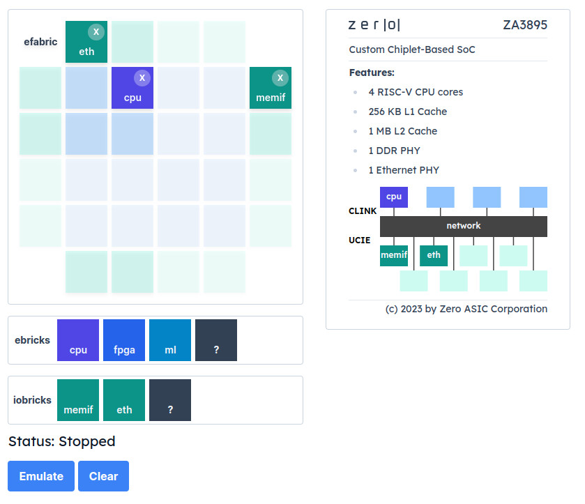
Moore Threads Prepares S90 and S4000 GPUs for Gaming and Data Center

Moore Threads Technology (MTT), a Chinese GPU manufacturer, is reportedly testing its next-generation graphics processors for client PCs and data centers. The products under scrutiny are the MTT S90 for client/gaming computers and the MTT S4000 for data centers. Characterized by their Device IDs, 0301 and 0323, this could imply that these GPUs belong to MTT's 3rd generation GPU lineup. While few details about these GPUs are available, the new Device IDs suggest a possible introduction of a novel microarchitecture following the MTT Chunxiao GPU series. The current generation Chunxiao series, featuring the MTT S70, MTT S80, and MTT S3000, failed to compete effectively with AMD, Intel, and NVIDIA GPUs.

Thanks to @Löschzwerg who found the Device Hunt submission, we see hardware identifiers in PCI ID and USB ID repositories earlier than launch, as this often signals the testing of new chips or drivers by various companies. In the case of MTT, the latest developments are complicated by its recent inclusion on the U.S. Entity List, limiting its access to US-made technologies. This introduces a problem for the company, as they can't access TSMC's facilities for chip production, and will have to turn to domestic production in the likely case, with SMIC being the only leading option to consider.

Zero ASIC Democratizing Chip Making

Zero ASIC, a semiconductor startup, came out of stealth today to announce early access to its one-of-a-kind ChipMaker platform, demonstrating a number of world firsts:
  • 3D chiplet composability enabling billions of new silicon products
  • Fully automated no-code chiplet-based chip design
  • Zero install interactive RTL-based chip emulation
  • Roadmap to 100X reduction in chip development costs
"Custom Application Specific Integrated Circuits (ASICs) offer 10-100X cost and energy advantage over commercial off the shelf (COTS) devices, but the enormous development cost makes ASICs non-viable for most applications," said Andreas Olofsson, CEO and founder of Zero ASIC. "To build the next wave of world changing silicon devices, we need to reduce the barrier to ASICs by orders of magnitude. Our mission at Zero ASIC is to make ordering an ASIC as easy as ordering catalog parts from an electronics distributor."

Arm and Synopsys Strengthen Partnership to Accelerate Custom Silicon on Advanced Nodes

Synopsys today announced it has expanded its collaboration with Arm to provide optimized IP and EDA solutions for the newest Arm technology, including the Arm Neoverse V2 platform and Arm Neoverse Compute Subsystem (CSS). Synopsys has joined Arm Total Design where Synopsys will leverage their deep design expertise, the Synopsys.ai full-stack AI-driven EDA suite, and Synopsys Interface, Security, and Silicon Lifecycle Management IP to help mutual customers speed development of their Arm-based CSS solutions. The expanded partnership builds on three decades of collaboration to enable mutual customers to quickly develop specialized silicon at lower cost, with less risk and faster time to market.

"With Arm Total Design, our aim is to enable rapid innovation on Arm Neoverse CSS and engage critical ecosystem expertise at every stage of SoC development," said Mohamed Awad, senior vice president and general manager, Infrastructure Line of Business at Arm. "Our deep technical collaboration with Synopsys to deliver pre-integrated and validated IP and EDA tools will help our mutual customers address the industry's most complex computing challenges with specialized compute."

Intel Partners with Submer to Cool 1,000+ Watt Processors using Immersion Cooling

Intel and Submer, a company specializing in immersion cooling, are set to unveil a creative immersion cooling system at the OCP Global Summit. This system can efficiently dissipate 1,000 W of power in a single-phase liquid cooling setup designed for deployment in data centers. Unlike traditional water cooling, immersion cooling systems offer higher efficiency and reliability. The solution developed by Submer and Intel is based on a Forced Convection Heat Sink (FCHS) and leverages a heat exchanger for heat transfer with a second liquid. The primary advantage of immersion cooling is its lack of active components on the cooling element, making it possible for immersed systems to operate without them for extended periods.

In this new system, a copper cooler is housed with two fans at one end to enhance liquid flow through the heat sink using forced convection. However, this active cooling component contradicts the traditional passive concept of immersion cooling based on natural convection. In its initial phase, Submer and Intel utilized Xeon processors with an 800 W TDP, with plans to increase that figure to 1,000 W in the next step. This Forced Convection Heat Sink (FCHS) offers the advantages of easy manufacturing and cost-effective usage while effectively dissipating up to 1,000 W of waste heat, making it a compelling option for immersion cooling. There are even possibilities of being 3D printed, according to Submer, and the plan is to achieve cooling of 1kW+ chip. We expect to hear more about the system during the OCP Global Summit, running from October 17 to 19, as currently, we only have a lower-resolution image from Submer's press release.

TSMC Announces Breakthrough Set to Redefine the Future of 3D IC

TSMC today announced the new 3Dblox 2.0 open standard and major achievements of its Open Innovation Platform (OIP) 3DFabric Alliance at the TSMC 2023 OIP Ecosystem Forum. The 3Dblox 2.0 features early 3D IC design capability that aims to significantly boost design efficiency, while the 3DFabric Alliance continues to drive memory, substrate, testing, manufacturing, and packaging integration. TSMC continues to push the envelope of 3D IC innovation, making its comprehensive 3D silicon stacking and advanced packaging technologies more accessible to every customer.

"As the industry shifted toward embracing 3D IC and system-level innovation, the need for industry-wide collaboration has become even more essential than it was when we launched OIP 15 years ago," said Dr. L.C. Lu, TSMC fellow and vice president of Design and Technology Platform. "As our sustained collaboration with OIP ecosystem partners continues to flourish, we're enabling customers to harness TSMC's leading process and 3DFabric technologies to reach an entirely new level of performance and power efficiency for the next-generation artificial intelligence (AI), high-performance computing (HPC), and mobile applications."

Winbond Introduces Innovative CUBE Architecture for Powerful Edge AI Devices

Winbond Electronics Corporation, a leading global supplier of semiconductor memory solutions, has unveiled a powerful enabling technology for affordable Edge AI computing in mainstream use cases. The Company's new customized ultra-bandwidth elements (CUBE) enable memory technology to be optimized for seamless performance running generative AI on hybrid edge/cloud applications.

CUBE enhances the performance of front-end 3D structures such as chip on wafer (CoW) and wafer on wafer (WoW), as well as back-end 2.5D/3D chip on Si-interposer on substrate and fan-out solutions. Designed to meet the growing demands of edge AI computing devices, it is compatible with memory density from 256 Mb to 8 Gb with a single die, and it can also be 3D stacked to enhance bandwidth while reducing data transfer power consumption.

TSMC Ramps Up CoWoS Advanced Packaging Production to Meet Soaring AI Chip Demand

The burgeoning AI market is significantly impacting TSMC's CoWoS (Chip on Wafer on Substrate) advanced packaging production capacity, causing it to overflow due to high demand from major companies like NVIDIA, AMD, and Amazon. To accommodate this, TSMC is in the process of expanding its production capacity by acquiring additional CoWoS machines from equipment manufacturers like Xinyun, Wanrun, Hongsu, Titanium, and Qunyi. These expansions are expected to be operational in the first half of the next year, leading to an increased monthly production capacity, potentially close to 30,000 pieces, enabling TSMC to cater to more AI-related orders. These endeavors to increase capacity are in response to the amplified demand for AI chips from their applications in various domains, including autonomous vehicles and smart factories.

Despite TSMC's active steps to enlarge its CoWoS advanced packaging production, the overwhelming client demand is driving the company to place additional orders with equipment suppliers. It has been indicated that NVIDIA is currently TSMC's largest CoWoS advanced packaging customer, accounting for 60% of its production capacity. Due to the surge in demand, companies like AMD, Amazon, and Broadcom are also placing urgent orders, leading to a substantial increase in TSMC's advanced process capacity utilization. The overall situation indicates a thriving scenario for equipment manufacturers with clear visibility of orders extending into the following year, even as they navigate the challenges of fulfilling the rapidly growing and immediate demand in the AI market.

Intel LGA-1851 "Arrow Lake" Socket Detailed

Thanks to the 3D renders and technical drawings obtained by Igor's Lab, we have insights into the structure of Intel's next-generation LGA-1851 socket for Arrow Lake processors. Scheduled to arrive in mid-2024, the LGA-1851 socket was originally intended for Meteor Lake-S desktop processors. However, the socket is now awaiting Arrow Lake since Meteor Lake is now a mobile-only processor generation. The first notable thing about LGA-1851 is that it will directly connect a dedicated PCIe 5.0 x4 interface to the CPU, besides the x16 lanes going to the GPU. This results in native support for high-speed PCIe 5.0 NVMe SSDs that can achieve speeds of over 12 GB/s in both read and write workloads.

Intel Arrow Lake-S will be available with eight P-cores and 16 E-cores in SKUs with different combinations of the two. The accompanying 800 series chipset includes Z890, B860, and H810 models, with an evident absence of H870 SKU. There will be W880 and Q870 workstation-grade chipsets as well. It is worth pointing out that Arrow Lake will enable DRAM capacities of up to 48 GB per DIMM at 6400 MT/s. We expect to hear more about Arrow Lake-S as we near the 2024 launch date and we get to see the Intel 20A node being used in client products. Below, you can see the technical drawings of the Independent Loading Mechanism (ILM) and chipset 3D models.

TSMC Could Delay 2 nm Mass Production to 2026

According to TechNews.tw, TSMC could postpone its 2 nm semiconductor manufacturing node for 2026. If the rumors about TSMC's delayed 2 nm production schedule are accurate, the implications could reverberate throughout the semiconductor industry. TSMC's alleged hesitancy could be driven by multiple factors, including the architectural shift from FinFET to Gate-All-Around (GAA) and potential challenges related to scaling down to 2 nm. The company is a crucial player in this space, and a delay could offer opportunities for competitors like Samsung, which has already transitioned to GAA transistor architecture for its 3 nm chips. Given the massive demand for advanced nodes due to the rise of AI, IoT, and other next-gen technologies, it is surprising to hear "sluggish" demand reports.

However, it's also possible that it's too early for customers to make firm commitments for 2025 and beyond. TSMC has dismissed these rumors, stating that construction is progressing according to plan, which includes having 2 nm pilot run in 2024, and mass production in the second half of 2025.. Despite this, any delay in TSMC's roadmap could serve as a catalyst for shifts in market dynamics. Companies that rely heavily on TSMC's advanced nodes might need to reassess their timelines and strategies. Moreover, if Samsung can capitalize on this opportunity, it could somewhat level the playing field. As of now, though, it's essential to approach these rumors with caution until more concrete information becomes available.

ITRI Leads Global Semiconductor Collaboration for Heterogeneous Integration to Pioneer Pilot Production Solutions

The introduction of Generative AI (GAI) has significantly increased the demand for advanced semiconductor chips, drawing increased attention to the development of complex calculations for large-scale AI models and high-speed transmission interfaces. To assist the industry in grasping the key to high-end semiconductor manufacturing and integration capabilities, the Heterogeneous Integrated Chiplet System Package (Hi-CHIP) Alliance brings together leading semiconductor companies from Taiwan and around the world to provide comprehensive services, spanning from packaging design, testing and verification, to pilot production. Since its establishment in 2021, the alliance has accumulated important industry players as its members, including EVG, Kulicke and Soffa (K&S), USI, Raytek Semiconductor, Unimicron, DuPont, and Brewer Science. Looking forward, the alliance is set to actively explore its global market potential.

Dr. Shih-Chieh Chang, General Director of Electronic and Optoelectronic System Research Laboratories at ITRI and Chairman of the Hi-CHIP Alliance, indicated that advanced manufacturing processes have led to a considerable increase in IC design cycles and costs. Multi-dimensional chip design and heterogeneous integrated packaging architecture are key tools to tackle this demand in semiconductors. On top of that, the advent of GAI such as ChatGPT, which demands substantial computing power and transmission speed, requires even higher levels of integration capacity in chip manufacturing. ITRI has been committed to developing manufacturing technologies and upgrading materials and equipment to enhance heterogeneous integration technologies. Achievements include the fan-out wafer level packaging (FOWLP), 2.5 and 3D chips, embedded interposer connections (EIC), and programmable packages. With both local and foreign semiconductor manufacturer members, the Hi-CHIP Alliance is establishing an advanced packaging process production line to provide an integrated one-stop service platform.

Intel Unveils Industry-Leading Glass Substrates to Meet Demand for More Powerful Compute

What's New: Intel today announced one of the industry's first glass substrates for next-generation advanced packaging, planned for the latter part of this decade. This breakthrough achievement will enable the continued scaling of transistors in a package and advance Moore's Law to deliver data-centric applications.

"After a decade of research, Intel has achieved industry-leading glass substrates for advanced packaging. We look forward to delivering these cutting-edge technologies that will benefit our key players and foundry customers for decades to come."
-Babak Sabi, Intel senior vice president and general manager of Assembly and Test Development

TSMC Prediction: AI Chip Supply Shortage to Last ~18 Months

TSMC Chairman Mark Liu was asked to comment on all things artificial intelligence-related at the SEMICON Taiwan 2023 industry event. According to a Nikkei Asia report, he foresees supply constraints lasting until the tail end of 2024: "It's not the shortage of AI chips. It's the shortage of our chip-on-wafer-on-substrate (COWOS) capacity...Currently, we can't fulfill 100% of our customers' needs, but we try to support about 80%. We think this is a temporary phenomenon. After our expansion of advanced chip packaging capacity, it should be alleviated in one and a half years." He cites a recent and very "sudden" spike in demand for COWOS, with numbers tripling within the span of a year. Market leader NVIDIA relies on TSMC's advanced packaging system—most notably with the production of highly-prized A100 and H100 series Tensor Core compute GPUs.

These issues are deemed a "temporary" problem—it could take around 18 months to eliminate production output "bottlenecks." TSMC is racing to bolster its native activities with new facilities—plans for a new $2.9 billion advanced chip packaging plant (in Miaoli County) were disclosed during summer time. Liu reckons that industry-wide innovation is necessary to meet growing demand through new methods to "connect, package and stack chips." Liu elaborated: "We are now putting together many chips into a tightly integrated massive interconnect system. This is a paradigm shift in semiconductor technology integration." The TSMC boss reckons that processing units fielding over one trillion transistors are viable within the next decade: "it's through packaging with multiple chips that this could be possible.".

MediaTek Successfully Develops First Chip Using TSMC's 3 nm Process, Set for Volume Production in 2024

MediaTek and TSMC today announced that MediaTek has successfully developed its first chip using TSMC's leading-edge 3 nm technology, taping out MediaTek's flagship Dimensity system-on-chip (SoC) with volume production expected next year. This marks a significant milestone in the long-standing strategic partnership between MediaTek and TSMC, with both companies taking full advantage of their strengths in chip design and manufacturing to jointly create flagship SoCs with high performance and low power features, empowering global end devices.

"We are committed to our vision of using the world's most advanced technology to create cutting edge products that improve our lives in meaningful ways," said Joe Chen, President of MediaTek. "TSMC's consistent and high-quality manufacturing capabilities enable MediaTek to fully demonstrate its superior design in flagship chipsets, offering the highest performance and quality solutions to our global customers and enhancing the user experience in the flagship market."

New MIPS CEO Sameer Wasson to Drive Company's RISC-V Market Penetration and Innovation

MIPS, a leading developer of high- performance RISC-V compute IP, has announced embedded systems industry veteran Sameer Wasson as the company's new CEO. Before joining MIPS, Wasson spent 18 years at Texas Instruments (TI), most recently as Vice President, Business Unit (BU) Manager, Processors, where he was responsible for the company's Processor businesses. In that role, Wasson re-established TI as a mainstream microprocessor (MPU) and microcontroller (MCU) supplier for high growth automotive and industrial markets, and established the company's footprint in embedded AI, software defined vehicles, and electrification.

As the new CEO of MIPS, Wasson will further accelerate the company's leadership in the High-Performance RISC-V market as it continues to expand its footprint in Automotive and Enterprise markets.

Samsung Electronics Unveils Industry's Highest-Capacity 12nm-Class 32Gb DDR5 DRAM

collaboration with diverse industries and support various applications
Samsung Electronics, a world leader in advanced memory technology, today announced that it has developed the industry's first and highest-capacity 32-gigabit (Gb) DDR5 DRAM using 12 nanometer (nm)-class process technology. This achievement comes after Samsung began mass production of its 12 nm-class 16Gb DDR5 DRAM in May 2023. It solidifies Samsung's leadership in next-generation DRAM technology and signals the next chapter of high-capacity memory.

"With our 12 nm-class 32Gb DRAM, we have secured a solution that will enable DRAM modules of up to 1-terabyte (TB), allowing us to be ideally positioned to serve the growing need for high-capacity DRAM in the era of AI (Artificial Intelligence) and big data," said SangJoon Hwang, Executive Vice President of DRAM Product & Technology at Samsung Electronics. "We will continue to develop DRAM solutions through differentiated process and design technologies to break the boundaries of memory technology."

Suppliers Successfully Hike Wafer Contract Prices, Triggering Short-Term Surge in NAND Spot Market

Recently, the spot market for NAND Flash chips has seen a rise in active price inquiries for certain products, a movement driven by successful increases in wafer contract prices. TrendForce reports this uptick primarily stems from negotiations in late August between NAND Flash suppliers and key Chinese module makers. These discussions led to a new wafer contract that successfully boosted the price of 512 Gb wafers by approximately 10%.

Other suppliers have also raised prices for their comparable products, signaling a shift in supplier sentiment: they are now less inclined to finalize deals at lower prices. This change has contributed to a short-term surge in the wafer spot market. Nevertheless, whether this surge in procurement is supported by actual end-user demand remains uncertain, as these orders have arisen in reaction to adjustments in supply-side pricing.

Intel Lists Testing Interposers for Arrow Lake-HX, Lunar Lake-M, and Battlemage

Intel recently updated its website to highlight interposers used for testing upcoming chips before their actual product integration. A specific webpage now showcases components used by various tools, notably the "Gen5 VR," which stands for CPU Voltage Regulator in this context. The highlight of the update reveals at least four yet-to-be-announced products: Battlemage (BMG), Arrow Lake (ARL), and Lunar Lake (LNL), slated for launch in 2024. Particularly interesting are the two Battlemage interposers: BGA2362-BMG-X2 and BGA2727-BMG-X3. This hints that a Battlemage GPU could have more pins than Intel's current top-tier GPU from the Alchemist series, known as DG2, which features 2660 pins (BGA2660-DG2-512EU).

This unveiling could indicate Intel's plans to introduce two GPUs in its new series or potentially two different package sizes. Manufacturers often use consistent package sizes for multiple GPUs, granting flexibility to interchange processors with similar specifications and presenting a feasible production strategy. Another notable mention is the Arrow Lake-HX, intended for premium desktop/laptop hybrids.. While there was some buzz about the ARL-HX series before, this update provides clear confirmation from Intel. Lastly, the reveal includes an interposer for the Lunar Lake-M series (LNL-M), which is expected to be Intel's most energy-efficient line. Drawing parallels from the Alder Lake series, such chips were designed for tablets with power consumption between 5 to 7 watts.

Intel Wants More Than its Fair Share of CHIPS Act Money

During the Aspen Security Forums 2023, Intel CEO Pat Gelsinger spoke on the topic of semiconductors and national security. During his speech, Gelsinger mentioned that Intel should get the lion's share of the US$52 billion US CHIPS Act money, simply because Intel is a US company. In Gelsinger's opinion, it appears that TSMC and Samsung don't deserve as much, despite both companies manufacturing semiconductors for US companies, with Samsung already having a foundry in Texas, while TSMC is still struggling with the construction of its Arizona foundry.

Admittedly, Intel has far more foundries in the US, but it also seems like Gelsinger forgot about other foundries, such as GlobalFoundries, but also companies such as Micron, Texas Instruments, Qorvo, NXP, On Semi, Analog Devices and so forth that all own foundries that produce their own chips on US soil. We'd expect all these companies to be eyeing the CHIPS Act cash and without many of those companies, Intel wouldn't be able to sell any of its chips, as many of them produce much needed components that are used to build motherboards, laptops and what not. Gelsinger was obviously pointing fingers at the current US China trade war and how the export controls are causing concerns with regards to the global semiconductor business. As such, Gelsinger wants Intel to have fewer restrictions from the currently imposed trade regulations, largely due to China being some 25 to 30 percent of Intel's market, with Intel being busy expanding in the country. Make what you want of this, but it's clear that Gelsinger is expecting to eat the cake and have it at the same time. Video after the break.

TSMC is Building a $10B Fab In Germany

TSMC (TWSE: 2330, NYSE: TSM), Robert Bosch GmbH, Infineon Technologies AG (FSE: IFX / OTCQX: IFNNY), and NXP Semiconductors N.V. (NASDAQ: NXPI) today announced a plan to jointly invest in European Semiconductor Manufacturing Company (ESMC) GmbH, in Dresden, Germany to provide advanced semiconductor manufacturing services. ESMC marks a significant step towards construction of a 300 mm fab to support the future capacity needs of the fast-growing automotive and industrial sectors, with the final investment decision pending confirmation of the level of public funding for this project. The project is planned under the framework of the European Chips Act.

The planned fab is expected to have a monthly production capacity of 40,000 300 mm (12-inch) wafers on TSMC's 28/22 nanometer planar CMOS and 16/12 nanometer FinFET process technology, further strengthening Europe's semiconductor manufacturing ecosystem with advanced FinFET transistor technology and creating about 2,000 direct high-tech professional jobs. ESMC aims to begin construction of the fab in the second half of 2024 with production targeted to begin by the end of 2027.

NEO Semiconductor to Present Its Ground-Breaking 3D NAND and 3D DRAM Architectures at Flash Memory Summit 2023

NEO Semiconductor, a leading developer of innovative technologies for 3D NAND flash and DRAM memory, today announced its participation at Flash Memory Summit 2023, taking place in person in Santa Clara, California, on August 8-10. CEO, Andy Hsu, will deliver a keynote address titled "New Architectures which will Drive Future 3D NAND and 3D DRAM Solutions" on August 9th at 11:40 a.m. Pacific Time.

Earlier this year, Neo Semiconductor announced the launch of its ground-breaking technology, 3D X-DRAM. This development is the world's first 3D NAND-like DRAM cell array that is targeted to solve DRAM's capacity bottleneck and replace the entire 2D DRAM market. 3D X-DRAM can be manufactured using the existing 3D NAND flash memory process with minor changes, significantly reducing the time and cost spent developing a new 3D process. During the keynote, Mr. Hsu will reveal the 3D X-DRAM process flow and technical details.

The European Union Council Approves Chips Act

The Council has today approved the regulation to strengthen Europe's semiconductor ecosystem, better known as the 'Chips Act'. This is the last step in the decision-making procedure. The Chips Act aims to create the conditions for the development of a European industrial base in the field of semiconductors, attract investment, promote research and innovation and prepare Europe for any future chip supply crisis. The programme should mobilise €43 billion in public and private investment (€3.3 billion from the EU budget), with the objective of doubling the EU's global market share in semiconductors, from 10% now to at least 20% by 2030.

With the Chips Act, Europe will be a frontrunner in the world semiconductors race. We can already see it in action: new production plants, new investments, new research projects. And in the long run, this will also contribute to the renaissance of our industry and the reduction of our foreign dependencies. - Héctor Gómez Hernández, Spanish Minister for Industry, Trade and Tourism

NVIDIA is Looking at Samsung for HBM3 Memory and 2.5D Chip Packaging

According to news out of Korea, NVIDIA is considering Samsung as a partner not only for HBM3 memory, but also as a potential partner when it comes to 2.5D chip packaging. The latter is due to TSMC having limited capacity when it comes to handling all of its customers advanced chip packaging needs, although Samsung is apparently not the only potential partner NVIDIA is looking at. Taiwan based SPIL and US based Amkor Technology are two alternative candidates for the 2.5D chip packaging according to the Elec.

As far as HBM3 memory goes, NVIDIA doesn't have as many potential options, with SK Hynix being its current partner, who NVIDIA will continue to work with when it comes to HBM memory for its high-end AI accelerators and GPUs. It's likely that Samsung is trying to win NVIDIA back as a foundry customer, by proving that it's capable of handling the chip packaging for NVIDIA. Samsung will likely use its I-Cube 2.5D packaging technology and the Elec suggests that Samsung would still be using TSMC made GPU wafers which will be mated with Samsung HMB3 memory. Samsung has as yet not started its mass production of HMB3 memory, but have sampled customers with evaluation samples that are said to have received very positive feedback. For now, nothing has been agreed and TSMC is, as we know, looking to expand its 2.5D packaging business by over 40 percent, but the question is how quickly TSMC can move before its customers consider other competitors.

DEEPX Announces State-of-the-Art AI Chip Product Lineup

DEEPX, a leading AI semiconductor technology company, aims to drive innovation in the rapidly evolving edge AI landscape with its state-of-the-art, low-power, high-performance AI chip product lineup. With a focus on revolutionizing application areas such as smart cities, surveillance, smart factories, and other industries, DEEPX unveiled its latest AI semiconductor solutions at the 2023 Samsung Foundry Forum (SFF), under the theme of "For AI Everywhere."

Recognizing the importance of collaboration and technological partnerships, DEEPX leveraged Samsung Electronics' foundry processes, harnessing the power of 5 nm, 14 nm, and 28 nm technologies for its semiconductor chip designs. As a result, the company has developed a suite of four high-performance, energy-efficient AI semiconductor products: DX-L1, DX-L2, DX-M1, and DX-H1. Each product has been specifically engineered to cater to the unique demands of various market segments, from ultra-compact sensors with minimal data processing requirements to AI-intensive applications such as robotics, computer vision, autonomous vehicles, and many others.

ASML Issues Statement Regarding Dutch Export Control Regulations

Today the Dutch government has published the new regulations regarding export controls of semiconductor equipment. As announced earlier in March, the new export controls focus on advanced chip manufacturing technology, including the most advanced deposition and immersion lithography systems.

Due to these export control regulations, ASML will need to apply for export licenses with the Dutch government for all shipments of its most advanced immersion DUV lithography systems (TWINSCAN NXT:2000i and subsequent immersion systems). The Dutch government will determine whether to grant or deny the required export licenses and provide further details to the company on any conditions that apply.

Samsung Electronics Unveils Foundry Vision in the AI Era

Samsung Electronics, a world leader in advanced semiconductor technology, today announced its latest foundry technology innovations and business strategy at the 7th annual Samsung Foundry Forum (SFF) 2023. Under the theme "Innovation Beyond Boundaries," this year's forum delved into Samsung Foundry's mission to address customer needs in the artificial intelligence (AI) era through advanced semiconductor technology.

Over 700 guests, from customers and partners of Samsung Foundry, attended this year's event, of which 38 companies hosted their own booths to share the latest technology trends in the foundry industry.
Return to Keyword Browsing
May 21st, 2024 11:56 EDT change timezone

New Forum Posts

Popular Reviews

Controversial News Posts