Monday, August 17th 2009

IBM Scientists Use DNA Scaffolding To Build Tiny Circuit Board
Today, scientists at IBM Research and the California Institute of Technology announced a scientific advancement that could be a major breakthrough in enabling the semiconductor industry to pack more power and speed into tiny computer chips, while making them more energy efficient and less expensive to manufacture.
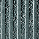
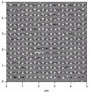
IBM researchers and collaborator Paul W.K. Rothemund, of the California Institute of Technology, have made an advancement in combining lithographic patterning with self assembly - a method to arrange DNA origami structures on surfaces compatible with today's semiconductor manufacturing equipment.Today, the semiconductor industry is faced with the challenges of developing lithographic technology for feature sizes smaller than 22 nm and exploring new classes of transistors that employ carbon nanotubes or silicon nanowires. IBM's approach of using DNA molecules as scaffolding - where millions of carbon nanotubes could be deposited and self-assembled into precise patterns by sticking to the DNA molecules - may provide a way to reach sub-22 nm lithography.
The utility of this approach lies in the fact that the positioned DNA nanostructures can serve as scaffolds, or miniature circuit boards, for the precise assembly of components - such as carbon nanotubes, nanowires and nanoparticles - at dimensions significantly smaller than possible with conventional semiconductor fabrication techniques. This opens up the possibility of creating functional devices that can be integrated into larger structures, as well as enabling studies of arrays of nanostructures with known coordinates.
"The cost involved in shrinking features to improve performance is a limiting factor in keeping pace with Moore's Law and a concern across the semiconductor industry," said Spike Narayan, manager, Science & Technology, IBM Research - Almaden. "The combination of this directed self-assembly with today's fabrication technology eventually could lead to substantial savings in the most expensive and challenging part of the chip-making process."
The techniques for preparing DNA origami, developed at Caltech, cause single DNA molecules to self assemble in solution via a reaction between a long single strand of viral DNA and a mixture of different short synthetic oligonucleotide strands. These short segments act as staples - effectively folding the viral DNA into the desired 2D shape through complementary base pair binding. The short staples can be modified to provide attachment sites for nanoscale components at resolutions (separation between sites) as small as 6 nanometers (nm). In this way, DNA nanostructures such as squares, triangles and stars can be prepared with dimensions of 100 - 150 nm on an edge and a thickness of the width of the DNA double helix.
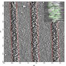
The lithographic templates were fabricated at IBM using traditional semiconductor techniques, the same used to make the chips found in today's computers, to etch out patterns. Either electron beam or optical lithography were used to create arrays of binding sites of the proper size and shape to match those of individual origami structures. Key to the process were the discovery of the template material and deposition conditions to afford high selectivity so that origami binds only to the patterns of "sticky patches" and nowhere else.
The paper on this work, "Placement and orientation of DNA nanostructures on lithographically patterned surfaces," by scientists at IBM Research and the California Institute of Technology, will be published in the September issue of Nature Nanotechnology and is currently available here.
Source:
IBM
IBM researchers and collaborator Paul W.K. Rothemund, of the California Institute of Technology, have made an advancement in combining lithographic patterning with self assembly - a method to arrange DNA origami structures on surfaces compatible with today's semiconductor manufacturing equipment.Today, the semiconductor industry is faced with the challenges of developing lithographic technology for feature sizes smaller than 22 nm and exploring new classes of transistors that employ carbon nanotubes or silicon nanowires. IBM's approach of using DNA molecules as scaffolding - where millions of carbon nanotubes could be deposited and self-assembled into precise patterns by sticking to the DNA molecules - may provide a way to reach sub-22 nm lithography.
The utility of this approach lies in the fact that the positioned DNA nanostructures can serve as scaffolds, or miniature circuit boards, for the precise assembly of components - such as carbon nanotubes, nanowires and nanoparticles - at dimensions significantly smaller than possible with conventional semiconductor fabrication techniques. This opens up the possibility of creating functional devices that can be integrated into larger structures, as well as enabling studies of arrays of nanostructures with known coordinates.
"The cost involved in shrinking features to improve performance is a limiting factor in keeping pace with Moore's Law and a concern across the semiconductor industry," said Spike Narayan, manager, Science & Technology, IBM Research - Almaden. "The combination of this directed self-assembly with today's fabrication technology eventually could lead to substantial savings in the most expensive and challenging part of the chip-making process."
The techniques for preparing DNA origami, developed at Caltech, cause single DNA molecules to self assemble in solution via a reaction between a long single strand of viral DNA and a mixture of different short synthetic oligonucleotide strands. These short segments act as staples - effectively folding the viral DNA into the desired 2D shape through complementary base pair binding. The short staples can be modified to provide attachment sites for nanoscale components at resolutions (separation between sites) as small as 6 nanometers (nm). In this way, DNA nanostructures such as squares, triangles and stars can be prepared with dimensions of 100 - 150 nm on an edge and a thickness of the width of the DNA double helix.
The lithographic templates were fabricated at IBM using traditional semiconductor techniques, the same used to make the chips found in today's computers, to etch out patterns. Either electron beam or optical lithography were used to create arrays of binding sites of the proper size and shape to match those of individual origami structures. Key to the process were the discovery of the template material and deposition conditions to afford high selectivity so that origami binds only to the patterns of "sticky patches" and nowhere else.
The paper on this work, "Placement and orientation of DNA nanostructures on lithographically patterned surfaces," by scientists at IBM Research and the California Institute of Technology, will be published in the September issue of Nature Nanotechnology and is currently available here.


51 Comments on IBM Scientists Use DNA Scaffolding To Build Tiny Circuit Board
The same thing can be demonstrated in reaction time tests by comparing experiments conducted at random intervals compared to constant intervals. At constant intervals, people practically catch it before it drops. At random intervals, they will barely catch it before it leaves their hands. Expectations are the difference between that wine glass falling on the floor shattering or someone catching it before it hits the floor.It has everything to do with the brain. The brain can execute a previous command much faster than learning a new one. Because baseball is all about reaction times, the brain's only decision is to swing or not to swing (ehm, execute, don't, or halt execution).We don't understand animals well enough to be certain of that. Yes, their ability to reason is vastly diminished compared to ours but they can still reason to a degree (especially primates).
My point is that computers exist because they succeed where humans do not--calculations. The very first computer was British and performed as a Nazi codebreaker. If you could just spit out what the square root of 1,234,567,890 is in under a second, we wouldn't need computers. At the same time, computers don't speak our biological language which is why they are a PITA to program. :laugh:
For instance, I was going to get the square root of that number for you but I can't find the damn square root button on the Windows calculator. So, I pound my chest like an ape, found my TI-89, turn a light on to see the screen, hit the keys, and finally get an answer: 35,140. If Math.Sqrt(1234567890) were already programmed into the computer, it could have told me the answer in less than 1/16th of a second. Likewise, I can tell the computer I hate it in less than 1/16th of second merely by punching it.
Computers and humans are alike in many ways but we see the world in very different ways: one explains everything in binary, the other explains everything in stories.
Back on topic, I'm excited that biology is being applied to computing. It is a lot of work for us to build machines that in turn builds processors. It would be much, much, much cheaper to have processors grow like weeds. XD
Just like computers and animals though, they mustn't have intelligence or else we'd be engineering a virus.