Monday, August 17th 2009

IBM Scientists Use DNA Scaffolding To Build Tiny Circuit Board
Today, scientists at IBM Research and the California Institute of Technology announced a scientific advancement that could be a major breakthrough in enabling the semiconductor industry to pack more power and speed into tiny computer chips, while making them more energy efficient and less expensive to manufacture.
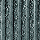
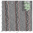
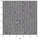
IBM researchers and collaborator Paul W.K. Rothemund, of the California Institute of Technology, have made an advancement in combining lithographic patterning with self assembly - a method to arrange DNA origami structures on surfaces compatible with today's semiconductor manufacturing equipment.Today, the semiconductor industry is faced with the challenges of developing lithographic technology for feature sizes smaller than 22 nm and exploring new classes of transistors that employ carbon nanotubes or silicon nanowires. IBM's approach of using DNA molecules as scaffolding - where millions of carbon nanotubes could be deposited and self-assembled into precise patterns by sticking to the DNA molecules - may provide a way to reach sub-22 nm lithography.
The utility of this approach lies in the fact that the positioned DNA nanostructures can serve as scaffolds, or miniature circuit boards, for the precise assembly of components - such as carbon nanotubes, nanowires and nanoparticles - at dimensions significantly smaller than possible with conventional semiconductor fabrication techniques. This opens up the possibility of creating functional devices that can be integrated into larger structures, as well as enabling studies of arrays of nanostructures with known coordinates.
"The cost involved in shrinking features to improve performance is a limiting factor in keeping pace with Moore's Law and a concern across the semiconductor industry," said Spike Narayan, manager, Science & Technology, IBM Research - Almaden. "The combination of this directed self-assembly with today's fabrication technology eventually could lead to substantial savings in the most expensive and challenging part of the chip-making process."
The techniques for preparing DNA origami, developed at Caltech, cause single DNA molecules to self assemble in solution via a reaction between a long single strand of viral DNA and a mixture of different short synthetic oligonucleotide strands. These short segments act as staples - effectively folding the viral DNA into the desired 2D shape through complementary base pair binding. The short staples can be modified to provide attachment sites for nanoscale components at resolutions (separation between sites) as small as 6 nanometers (nm). In this way, DNA nanostructures such as squares, triangles and stars can be prepared with dimensions of 100 - 150 nm on an edge and a thickness of the width of the DNA double helix.
The lithographic templates were fabricated at IBM using traditional semiconductor techniques, the same used to make the chips found in today's computers, to etch out patterns. Either electron beam or optical lithography were used to create arrays of binding sites of the proper size and shape to match those of individual origami structures. Key to the process were the discovery of the template material and deposition conditions to afford high selectivity so that origami binds only to the patterns of "sticky patches" and nowhere else.
The paper on this work, "Placement and orientation of DNA nanostructures on lithographically patterned surfaces," by scientists at IBM Research and the California Institute of Technology, will be published in the September issue of Nature Nanotechnology and is currently available here.
Source:
IBM
IBM researchers and collaborator Paul W.K. Rothemund, of the California Institute of Technology, have made an advancement in combining lithographic patterning with self assembly - a method to arrange DNA origami structures on surfaces compatible with today's semiconductor manufacturing equipment.Today, the semiconductor industry is faced with the challenges of developing lithographic technology for feature sizes smaller than 22 nm and exploring new classes of transistors that employ carbon nanotubes or silicon nanowires. IBM's approach of using DNA molecules as scaffolding - where millions of carbon nanotubes could be deposited and self-assembled into precise patterns by sticking to the DNA molecules - may provide a way to reach sub-22 nm lithography.
The utility of this approach lies in the fact that the positioned DNA nanostructures can serve as scaffolds, or miniature circuit boards, for the precise assembly of components - such as carbon nanotubes, nanowires and nanoparticles - at dimensions significantly smaller than possible with conventional semiconductor fabrication techniques. This opens up the possibility of creating functional devices that can be integrated into larger structures, as well as enabling studies of arrays of nanostructures with known coordinates.
"The cost involved in shrinking features to improve performance is a limiting factor in keeping pace with Moore's Law and a concern across the semiconductor industry," said Spike Narayan, manager, Science & Technology, IBM Research - Almaden. "The combination of this directed self-assembly with today's fabrication technology eventually could lead to substantial savings in the most expensive and challenging part of the chip-making process."
The techniques for preparing DNA origami, developed at Caltech, cause single DNA molecules to self assemble in solution via a reaction between a long single strand of viral DNA and a mixture of different short synthetic oligonucleotide strands. These short segments act as staples - effectively folding the viral DNA into the desired 2D shape through complementary base pair binding. The short staples can be modified to provide attachment sites for nanoscale components at resolutions (separation between sites) as small as 6 nanometers (nm). In this way, DNA nanostructures such as squares, triangles and stars can be prepared with dimensions of 100 - 150 nm on an edge and a thickness of the width of the DNA double helix.
The lithographic templates were fabricated at IBM using traditional semiconductor techniques, the same used to make the chips found in today's computers, to etch out patterns. Either electron beam or optical lithography were used to create arrays of binding sites of the proper size and shape to match those of individual origami structures. Key to the process were the discovery of the template material and deposition conditions to afford high selectivity so that origami binds only to the patterns of "sticky patches" and nowhere else.
The paper on this work, "Placement and orientation of DNA nanostructures on lithographically patterned surfaces," by scientists at IBM Research and the California Institute of Technology, will be published in the September issue of Nature Nanotechnology and is currently available here.


51 Comments on IBM Scientists Use DNA Scaffolding To Build Tiny Circuit Board
Too true, and I guess neither the Acer or Dell terminator would get very far with its cheap plastic outer shell / body armor.
Maybe having a budget oriented company manufacturing walking death machines wouldn't be so bad.
and apply it to a bunch of terminators.
arstechnica.com/science/news/...cal-fluids.ars
ie
a computer can chomp out a complex math equation in a matter of seconds, where a human brain would take minutes, hours, maybe even days
but
a computer cannot process the the shear amount of data that would come from all 5 of our senses, process it, and still have power to respond and make complex rational decisions, where as a human brain can
besides, arent computers lack of being able to process local motion, or one of the five senses, merely stemming from lack of attached hardware(as in the inner ear in the case of balance, or a nose in the case of one of the senses) and ai/software as efficient as our nervous system?
not trying to argue, now im just curious
am i wrong?
I don't know how many odours a nose can smell at once however, but to process as fast as humans, a machine would probably need 1 thread for every 1 or 2 scents. This way it can process the scent, access a database on various scents, and then start matching up to that scent. Now apply that similar thinking to every sense. Touch depends on nerve placement. For example, a finger can differentiate between 2 contacts within millimeters of each other where as the side of your arm is maybe more like 2 contacts within an inch of each other. You'd need to apply the same sort of logic as we did for smell, because when you feel something, you immediately assess it. Sharp and ouchy? Pull away. Warm and burny? Pull away. Soft and harmless? ... Damnit. Its a trap! Pull away. Etc.
Anyways, coming down to it, I'd think a computer would have to be massively threaded to process all the info that humans can at once. Mind you, the key operator in my statement is 'can'. Most people can't seem to walk and talk at the same time, so maybe it'd be easier to build a computer to mimic them. :laugh:
Take a girl, add K&Y and you have fun.
Take a computer, add K&Y and I don't care what kind of CPU or DNA it has and you end up with problems.