Wednesday, April 21st 2010

Intel Sandy Bridge to Introduce New Sockets, Chipsets, Reorganize Platform Further
Intel plans a pair of new sockets for launch with its new processor architecture that succeeds Westmere, codenamed "Sandy Bridge", which are due for 2011. As part of its "tick-tock" product launch strategy, the company is currently transitioning between the 45 nm "tock" (Nehalem architecture), and 32 nm "tick" (Westmere architecture). In 2011, it will transition from the 32 nm "tick" (Westmere architecture), to the 32 nm "tock" (Sandy Bridge architecture). The company uses a "tick-tock" model of process development, where each processor architecture gets to be made in two successive manufacturing processes, while each process gets to build two succeeding architectures. It seems to have become clear that with Sandy Bridge, Intel will also switch to new socket designs, making existing motherboards obsolete then. Architecturally, Sandy Bridge will introduce new feature-sets that make the CPU more powerful, clock-to-clock, such as AVX - Advanced Vector Extensions, an evolution of the SSE instruction set, native AES engine which has been introduced with Westmere, and so on.
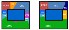
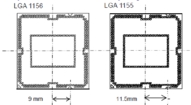
The present LGA-1156 package on which Intel builds value-through-performance processors including a bulk of mainstream processors, will be succeeded with the LGA-1155 package. Though similar, LGA-1155 and LGA-1156 are not inter-compatible, meaning that LGA-1155 processors will not work on existing LGA-1156 motherboards, and LGA-1156 processors will not work on LGA-1155 motherboards, either. For these processors, the arrangement of vital components is similar to the LGA-1156 package, except that every LGA-1155 processor - dual-core or quad-core - will feature an on-die display controller.The die itself will be monolithic, where the northbridge component completely integrates with the processor component, leaving only the southbridge outside the package, on the motherboard. Currently, the "Clarkdale" and "Arrandale" dual-core processors have the processor and northbridge components on separate dies, but on the same package. LGA-1155 is also designated as socket H2 (LGA-1156 is H1), the package is identical in size to LGA-1156, but has a different pin layout and orientation notch.Chipsets that drive the LGA-1156 platform include P67, H67, H61, and Q67, which will support features which were conceived prior to Ibex Peak platform's launch, but were shelved, such as ONFI NAND Flash "Braidwood", etc. USB 3.0 still isn't part of the feature-set, though native SATA 6 Gb/s support is on the cards.
The next big platform to succeed the LGA-1366, which caters to processors in the upper performance-though-enthusiast segments is the "Patsburg" platform, succeeding the existing "Tylersburg" based Intel X58, 5000 series chipsets. Here, Intel will introduce a massive new socket, the LGA-2011. The pin count is drastically increased for two reasons: the processor will have a 256-bit wide memory interface (quad-channel DDR3), and the northbridge component (currently X58 PCH) will be integrated completely into the processor package, upping the pin count with the PCI-Express and DMI pins. The on-die PCI-Express 2.0 root-complex will give out 32 lanes for graphics (unlike 16 lanes on the LGA-1155), and a DMI link to the so-called "Intel X68" chipset, which is relegated to being a Platform Controller Hub, just like the P55, or P67. The X68 could have a feature-set similar to the P67.
Source:
bit-tech.net
The present LGA-1156 package on which Intel builds value-through-performance processors including a bulk of mainstream processors, will be succeeded with the LGA-1155 package. Though similar, LGA-1155 and LGA-1156 are not inter-compatible, meaning that LGA-1155 processors will not work on existing LGA-1156 motherboards, and LGA-1156 processors will not work on LGA-1155 motherboards, either. For these processors, the arrangement of vital components is similar to the LGA-1156 package, except that every LGA-1155 processor - dual-core or quad-core - will feature an on-die display controller.The die itself will be monolithic, where the northbridge component completely integrates with the processor component, leaving only the southbridge outside the package, on the motherboard. Currently, the "Clarkdale" and "Arrandale" dual-core processors have the processor and northbridge components on separate dies, but on the same package. LGA-1155 is also designated as socket H2 (LGA-1156 is H1), the package is identical in size to LGA-1156, but has a different pin layout and orientation notch.Chipsets that drive the LGA-1156 platform include P67, H67, H61, and Q67, which will support features which were conceived prior to Ibex Peak platform's launch, but were shelved, such as ONFI NAND Flash "Braidwood", etc. USB 3.0 still isn't part of the feature-set, though native SATA 6 Gb/s support is on the cards.
The next big platform to succeed the LGA-1366, which caters to processors in the upper performance-though-enthusiast segments is the "Patsburg" platform, succeeding the existing "Tylersburg" based Intel X58, 5000 series chipsets. Here, Intel will introduce a massive new socket, the LGA-2011. The pin count is drastically increased for two reasons: the processor will have a 256-bit wide memory interface (quad-channel DDR3), and the northbridge component (currently X58 PCH) will be integrated completely into the processor package, upping the pin count with the PCI-Express and DMI pins. The on-die PCI-Express 2.0 root-complex will give out 32 lanes for graphics (unlike 16 lanes on the LGA-1155), and a DMI link to the so-called "Intel X68" chipset, which is relegated to being a Platform Controller Hub, just like the P55, or P67. The X68 could have a feature-set similar to the P67.


119 Comments on Intel Sandy Bridge to Introduce New Sockets, Chipsets, Reorganize Platform Further
It's just not been nearly as often..and when people got upset and cried about it AMD got the message (to a point) and yet they will be doing a Socket change here pretty soon as well..But AM2/AM2+/AM3 will have lasted about 5 years..
Hey Don't get me wrong I like that Intel does this, as it keeps the average Joe confused as to what works with what, and gives people a Jobs, it's just not for me..
I applause Intel for advancing the industry and for us it shouldn't make any difference. Why? Because we change our rigs every other year anyways!
Also if you get to brass tacts what takes advantage of an i7 currently? I mean what really makes them scream for mercy?...........yeah thats what I thought.
I use the Tick-Tock as well but for me it's CPU-tick-hard drives-tock Video Card-tick Memory-tock
The other thing is, AMD is most likely (like 99% chance) going to bring out a new socket for Fusion because I personally see no way they can manage to bring out that many features and not upgrade socket, and I can see now that Intel has moved the IOH/MCH into the CPU, this will happen alot now due to features that would have been added to the IOH/MCH that could have been a simple motherboard update now require a full on socket change.
Don't get me wrong, I think it's ridiculous they had to go and change so damned quickly, but when you really think about it, Intel has never been a cheap processor manufacturer. They have always been just the best. It's as simple as that.
The app attached to this post will make any processor (or multiple processors) beg for mercy for five minutes.
Gaming only uses 3-4 cores at most.
Office work is fine on 1 core.
New games may use all 8 cores but 4 of which are at barely more than idle. Any software that does something and fully loads 8 cores means it will take twice as long on a quad core, four times as much on a dual cores, and so on. Programmers try to avoid creating that much strain on systems unless it is unavoidable (like BOINC/F@H) or intentional (like the app I linked to).
I wrote a multithreaded application for benchmarking using a simple counting scheme. Performance was in excess of four times better with hyperthreading enabled than not. SMT, when done right, means the actual number of cores is irrelevent. The more data thrown on to the CPU as a whole the better the performance.
On applications that aren't heavily multithreaded, the architecture of Core i# is inferior to that of Core 2 and Phenom II.
I'm curious though, out of say the top 100 commercial programs (just picking a number here) what percentage would scale the way the counting program you wrote, at >4x faster with hyperthreading than without? I'd imagine the percentage would be pretty small?
[Intel Core i7 Inside Logo]
QUAD-CORE
DESKTOP
INTEL CORE i7 PROCESSOR
Also about the whole Core 2s being better than Core i7s in poorly threaded apps, it's simply not true. I wrote a program years ago for comparing P4s and it tests the CPUs per thread performance, and per MHz, Nehalem is faster than Core. Can't remember exact numbers, but if memory serves me right my old Core 2 E8400 at 3.0GHz got the same score as a Core i7 920 at 2.6GHz.
What makes my app unique is that, theoretically, it can linger in the L1/L2 caches of the processor eliminating the bottleneck on Core 2 machines (extra latency from going to the North Bridge, the RAM, and back again). Low scores (like my Core i7 920 without Hyperthreading) are most likely caused by cache collisions where the core(s) had to run all the way to the RAM instead of staying on the processor. Little faults like that is all it takes to get ahead.
I highly doubt Intel would be dumb enough to release a chip worse than it's predecessor after the fiasco they had with Netburst.
Bottom line: i7 is more powerful in every way, multi or single threaded.