Tuesday, June 22nd 2010

New NVIDIA GF100 Board Surfaces, Suggests New High-End SKU
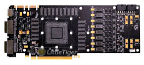
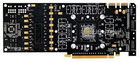
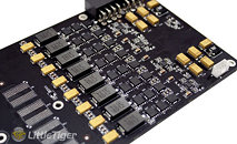
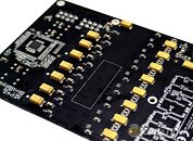
Sources in the hardware industry leaked some interesting pictures of a new, supposedly reference-design NVIDIA GF100 GPU graphics card PCB, watermarked by board partner Little Tiger. The pictures reveal a PCB that's similar to that of the GeForce GTX 480, but with a stronger VRM that makes use of better high-C surface-mount capacitors (completely doing away with cylindrical capacitors), and draws power from two 8-pin PCI-Express power inputs. The design can deliver up to 375W of power (that's not the board power we're talking about).
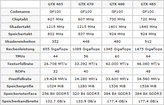
This also opens up speculation about what NVIDIA would do with this design. The most talked about theory as of now points to a new high-end SKU by NVIDIA based on the GF100, that enables all streaming multiprocessors (SMs) physically present on the GF100, taking the CUDA core count up to 512, and ROP count to 64. The most likely marketing name for this SKU is GeForce GTX 485. Apart from higher CUDA core and ROP count than that of the GTX 480, slightly higher clock-speeds for the GPU are also on the cards. The memory subsystem remains untouched, at 1536 MB of GDDR5 memory clocked at 924 MHz (effective 3.7 GHz), over a 384-bit wide memory interface. NVIDIA could release this SKU this fall.
Sources:
Hardware-Infos, Expreview
This also opens up speculation about what NVIDIA would do with this design. The most talked about theory as of now points to a new high-end SKU by NVIDIA based on the GF100, that enables all streaming multiprocessors (SMs) physically present on the GF100, taking the CUDA core count up to 512, and ROP count to 64. The most likely marketing name for this SKU is GeForce GTX 485. Apart from higher CUDA core and ROP count than that of the GTX 480, slightly higher clock-speeds for the GPU are also on the cards. The memory subsystem remains untouched, at 1536 MB of GDDR5 memory clocked at 924 MHz (effective 3.7 GHz), over a 384-bit wide memory interface. NVIDIA could release this SKU this fall.
75 Comments on New NVIDIA GF100 Board Surfaces, Suggests New High-End SKU
I have read somewhere i really can't remember, that all these 3 cards, which will be the lower line of the series, will come out before the end of 2010 (in fact that was in a graph)
All other top of the line cards will come out in 2011
Ultra off topic :D
im guessing no one has seen this yet?
Over at EXPreview, some photographs have surfaced of the shortened version of the GTX 480. This PCB design appears to be a complete redesign of the GTX 480 that we recently reviewed from Nvidia. The interesting thing is, these designs are beginning to surface before cards are even globally available through retailers. This fact brings us to believe that AIBs have been working on these designs for quite some time and that a redesign has long been in the cards.
Taiyanfa Custom GeForce GTX 480 Board - an ideal board for Folding@home?
Taiyanfa Custom GeForce GTX 480 Board - an ideal board for Folding@home and powerful HTPC systems?
This non-reference card appears to feature not only a shorter card length, but it also should have dual 6-pin power connectors as opposed to the current 8 + 6 pin design. In addition to that, there is a possibility that these cards could launch at the same clocks as the reference cards but possibly be hampered in overclocking by their dual 6 pin design. This design is drastically different from even the first custom PCB cards that we reported on around the time of the GTX 480 launch.
Backside of this custom PCB design reveals how short the GTX 480 design can be - this board is as short as GeForce GTS 250
Backside of this custom PCB design reveals how short the GTX 480 design can be - this board is as short as GeForce GTS 250
As we’ve stated before in our GTX 480 review, there will likely be a ton of custom PCB designs out there that could possibly help Nvidia stay in the game, although as it stands right now there still aren’t any GTX 480’s out there for sale yet and the card is indeed quite hot and power hungry. AIBs hope to remedy both of these issues with custom coolers and non-reference designs.
Taiyanfa's custom design PCB lowers the maximum power consumption to 225W [75W from PCIe x16, two 6-pin connectors count for additional 150W total], which is most probably achieved by lowering the GPU clock. However, we see a lot of potential in this design - for instance, populating six PCIe slots on All-PCIe boards such as ASUS P6T6/P6T7 or EVGA's X58 Classified 4-Way SLI for a GPGPU computing monster, single card design for HTPC chassis, or simply users that don't have 8+6-pin power - such as numerous workstation chassis or already assembled computers from Dell, HP and the like.
Source
(but i hope its not turn to shitty port :cry:)
:)
www.gigabyte.com/MicroSite/95/components.html#com5