Wednesday, February 22nd 2012

Ivy Bridge Die Layout Estimated
Hiroshige Goto, contributor for PC Watch that is known for detailed schematics of dies estimated the layout of Ivy Bridge silicon. Ivy Bridge is Intel's brand new multi-core processor silicon built on its new 22 nanometer silicon fabrication process. The four core silicon, which four configurations can be carved, will be built into packages that are pin-compatible with today's Sandy Bridge processors. The die area of Ivy Bridge is 160 mm², it has a total transistor count of 1.48 billion, compared to the Sandy Bridge silicon, which has 1.16 billion transistors crammed into a die 216 mm² in area, built on the 32 nm process.
Ivy Bridge has essentially the same layout as Sandy Bridge. The central portion of the die has four x86-64 cores with 256 KB dedicated L2 cache each, and a shared 8 MB L3 cache, while either sides of the central portion has the system agent and the graphics core. All components are bound by a ring-bus, that transports tagged data between the four CPU cores, the graphics core, the L3 cache, and the system agent, which has interfaces for the dual-channel DDR3 integrated memory controller, the PCI-Express controller, and the DMI chipset bus. Intel can carve four main configurations out of this silicon:
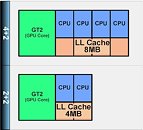
As mentioned earlier, all components on the silicon are bound by a ring-bus that transports data and instructions between the components. This bus has "ring-stops" from where it picks up and drops off data. The graphics core packs up to 16 programmable EUs that handle parallel processing loads for the GPU, they can also be programmed to perform GPGPU tasks. The system agent holds a dual-channel DDR3 integrated memory controller (IMC), a PCI-Express interface that gives out two x8 ports that can work as a single PCI-Express x16, or switched as two x8 ports; a DMI link to the PCH, a display controller, and FDI link to the PCH. Overall, Intel managed to make more efficient use of its die space.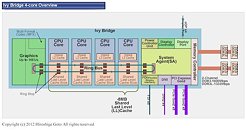
Source:
PC Watch
Ivy Bridge has essentially the same layout as Sandy Bridge. The central portion of the die has four x86-64 cores with 256 KB dedicated L2 cache each, and a shared 8 MB L3 cache, while either sides of the central portion has the system agent and the graphics core. All components are bound by a ring-bus, that transports tagged data between the four CPU cores, the graphics core, the L3 cache, and the system agent, which has interfaces for the dual-channel DDR3 integrated memory controller, the PCI-Express controller, and the DMI chipset bus.

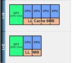
- 4+2: All four cores enabled, full 8 MB L3 cache enabled, all 16 shader cores (EUs) of the IGP enabled
- 4+1: All four cores enabled, 6 MB L3 cache enabled, fewer shader cores of the IGP enabled
- 2+2: Two cores enabled, 4 MB L3 cache enabled, all 16 shader cores of the IGP enabled
- 2+1: Two cores enabled, 3 MB L3 cache enabled, fewer shader cores of the IGP enabled


18 Comments on Ivy Bridge Die Layout Estimated
INTEL's profit margins to hit a new high this year
Now the GPU eventually taking up more space...yeah I can see that coming as CPUs and GPU tech merge even more.
www.techpowerup.com/160895/Core-i5-3570K-Graphics-67-Faster-Than-Core-i5-2500K-36-Slower-Than-GeForce-GT-240.html
And shader count doesn't mean anything when you compare different architectures.
1) in the IB layour schematic(165d), the PCIe lanes say "gen2", since IB is gen3, why is that?
2) this is more of a design oddity that i can't make sense of compared to SB: why are the display outputs on the SA(FDI, eDP, DAC) furthest from the graphics core?.
i mean, when you're processing graphics/video decode, now the data first has to go through the ring to the GPU, THEN COME BACK through the entire ring back to the SA to be outputted?.
My deduction on that design call is that once the data is processed and in the (main ram) framebuffer then it makes sense to have the display outputs on the SA side as they'd only need to access the ram address space -which is in the same SA so not neededing a full ring access-...
if it where on the GPU side like SB, then you'd need 3 ring accesses, once to get data to the gpu, another to put data in framebuffer and another to readback the framebuffer to display outputs.
Intel HD4000 should be much better than Nvidia 8400GS and ATI HD5450, and those are the only ones that cost around ~ $30
And for laptops, the price of equivalent dedicated GPU is even higher.
An In-efficient 100 shaders would get blown away by 50 efficient shaders.
SNB already has eDP onboard, the next step would be to directly forego the FDI and have all -digital- display outputs(i think the fdi is there for DVI and HDMI and analog VGA), a single/dual DP output.
BTW: they might release non-GPU(or actually, gpu silicon laser-disabled at the fab) versions like they currently do with normal SNB.
And apart from SNB-E that doesn't has onboard gpu, the entire Xeon line won't have integrated gpu either
The Ivy Bridge dual core die with 4MB L3 and HD4000 graphics will be approximately 118mm2. Despite a two node manufacturing advantage, Ivy Bridge dual cores are still larger than Wolfdale. There will probably also be another Ivy dual core die with 3MB L3 and HD 2500 with a die size below 100 mm2.
Given that Haswell is still on 22nm, has a larger GPU than Ivy, and supposedly has 1MB L2 cache per core (vs 256k), I expect there will still be native dual core dies.